NXP Semiconductors has announced the industry’s first crossover MCU, i.MX RT1170 28nm fully-depleted silicon-on-insulator (FD-SOI) microcontroller unit (MCU), which is a power-efficient design with real-time functionality, and MCU usability at an affordable price. It clocks its primary Arm Cortex-M7 processing core at up to 1GHz while packing a secondary Cortex-M4 core running at 400MHz. Geoff Lees, senior vice president and general manager for microcontrollers at NXP says:
“NXP saw the potential early on to create high-performance crossover MCUs, utilising the latest applications processor architecture and design philosophies. Now, with the i.MX RT1170 breaking the gigahertz barrier, we have opened up edge computing to all these technology possibilities.”
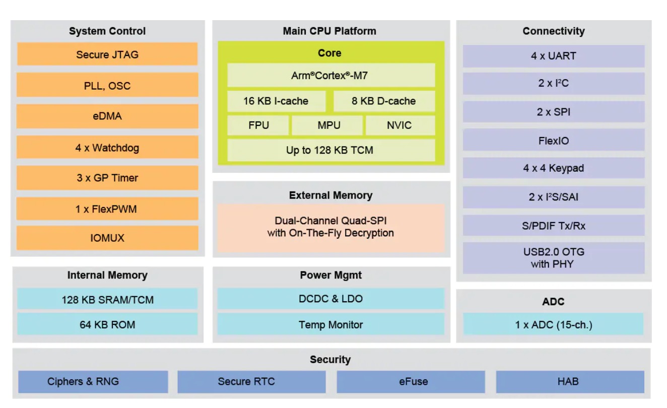
In addition to its Cortex-M7 and Cortex-M4 cores, the i.MX RT1170 features a 2D vector graphics core, NXP‘s in-house Pixel Processing Pipeline (PxP) 2D graphics accelerator, and its EdgeLock 400A embedded security platform. The new crossover MCU incorporates up to 2MB of on-chip SRAM, including 512KB that can be configured as TCM with Error Code Correction (ECC) for Cortex-M7 use, and 256KB of TCM with ECC for Cortex-M4 use.
The i.MX RT1170 dual-core system infuses a high-performance core and a power-efficient core with independent power domains of operation, enabling developers to run applications in parallel or reduce power consumption by switching off individual cores as necessary. To illustrate, the energy-efficient Cortex-M4 core can be dedicated to time-critical control applications, such as sensor hub and motor control, while the main core runs more complex applications. Additionally, its dual-core system can run ML applications in parallel, such as face recognition with natural language processing to create human-like user interactivity.
i.MX RT1170 Crossover MCU Block Diagram
As we move towards a world of a trillion connected devices, businesses are looking for real-time data insights, driving an increased requirement for on-device intelligence,”
says Dipti Vachani, senior vice president and general manager for automotive and Internet of Things (IoT) at core IP provider Arm. He continues :
“The i.MX RT1170 family efficiently combines enhanced on-device processing with low-latency performance, significantly lowering the bill of materials (BOM) cost, while pushing the boundaries of what’s possible for embedded and IoT applications.”
For edge compute applications, the GHz Cortex-M7 core enhances performance for ML, edge inference for voice, vision and gesture recognition, natural language understanding, data analytics, and digital signal processing (DSP) functions. The combination of GHz performance and high density of on-chip memory speeds up face recognition inference time by up to 5x, in comparison to today’s fastest MCUs available in the market, in addition to having processing bandwidth to improve accuracy and immunity against spoofing. The GHz core is also highly efficient in executing computationally demanding voice recognition, including audio pre-processing (echo cancellation, noise suppression, beamforming, and barge-in) for improved cognition. The GHz core also offers 720p displays at 60fps refresh and 1080p HD screens at 30fps to create immersive visual experiences. The combination of a GPU and high-performance core can be useful for smart home, industrial, and automotive cockpit applications.
NXP has confirmed it will be demonstrating the i.MX RT1170 at Arm TechCon 2019, showcasing a new record CoreMark benchmark run of 6,468 at Booth #731 on October 8th-10th 2019. More information on the part itself can be found on the NXP website.
The electrons movement in electronic components lead to the generation of heat which when beyond certain thresholds, prevents some components from functioning properly and in others could lead to a catastrophic breakdown. For this reason, the topics of ventilation, overheating, and cooling are important discussions in the design of any device. Several cooling solutions, including popular ones like; the use of aluminum heat sinks, and fans/heat extractor can be adopted for a project but the ultimate choice usually depends on the amount of heat produced and the maximum level the components can withstand. Heat extractors/fans are used in devices like Laptop computers and similar in which the amount of heat being generated could get really high. To save power and reduce noise levels, the fans are deployed in a feedback-based system such that the they only come on when certain heat threshold is attained and goes back off when heat levels are back to normal. For today’s tutorial, we will examine how a DIY version of this temperature-controlled fan can be built and deployed in your electronics project.
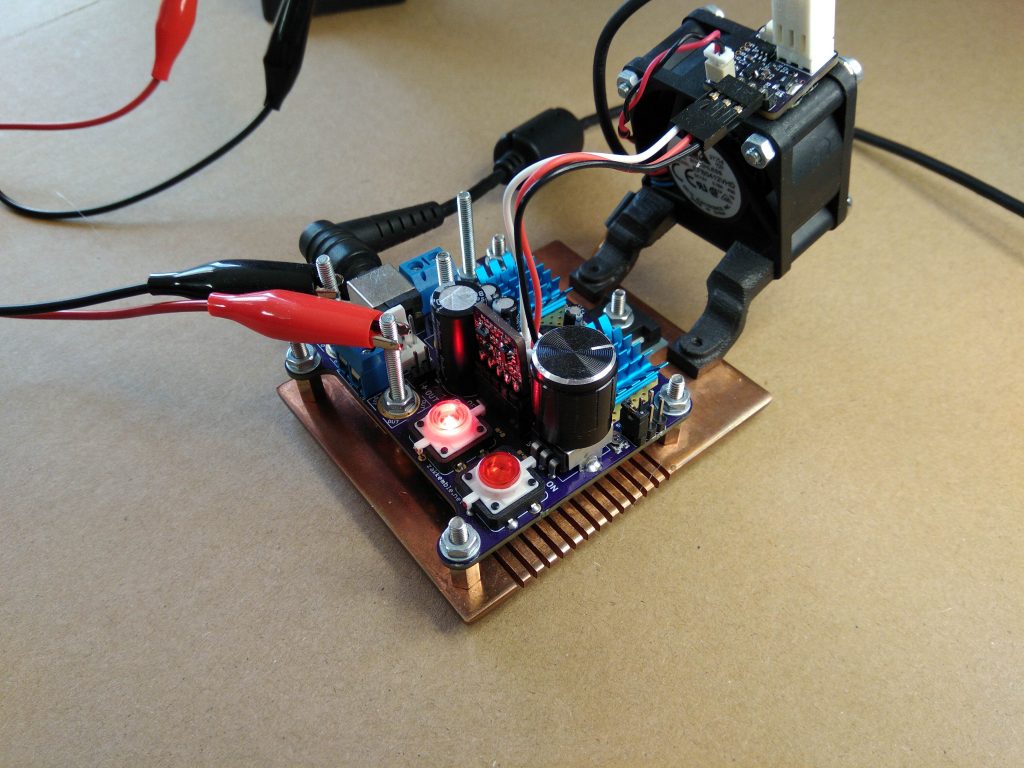
While there are several solutions for this issue on the internet, this project will chronicle the efforts of Zak Kemble during the construction of his bench power supply due to the compact and standalone module-like nature of his build.
At the end of the tutorial, you will be able to build a microcontroller based FAN controller to be used in your electronic devices.
Required Components
The following components are required to build this project;
A more comprehensive BOM generated from the schematics is provided in the table below. Since the project is expected to be deployed in a device, the decision was made to use mostly SMD-type components as it will help reduce space occupied by the device.
Part
Value
Device
Package
Description
C1
1u
CAP_CERAMIC_0603MP
_0603MP
Ceramic Capacitors
C2
1u
CAP_CERAMIC_0603MP
_0603MP
Ceramic Capacitors
C3
1n
CAP_CERAMIC0402_SMALL
0402_SMALL
D1
1N4148WT
DIODESOD-523
SOD-523
Diode in 0805 package
JP1
PINHD-1X3
1X03
PIN HEADER
JP4
2WAY
2WAY
Q1
DMG6968U-7
MOSFET-NWAVE
SOT23-W
N-Channel Mosfet
R1
10k
RESISTOR0402_SMALL
0402_SMALL
R2
100R
RESISTOR0402_SMALL
0402_SMALL
R3
10k
RESISTOR0402_SMALL
0402_SMALL
SW1
SPST_TACTG75_3X4
TACT_SMD5
U1
ATTINY10
ATTINY10SM_PAD
SOT23-6_SM_PAD
U2
MCP1703T-5002E/CB
MCP1700T-2502E/TTWIDE_PAD
SOT-23
Low Quiescent Current LDO
X1
22-23-2031
22-23-2031
22-23-2031
0.1
All of these components can be bought from electronics component suppliers like digikey.
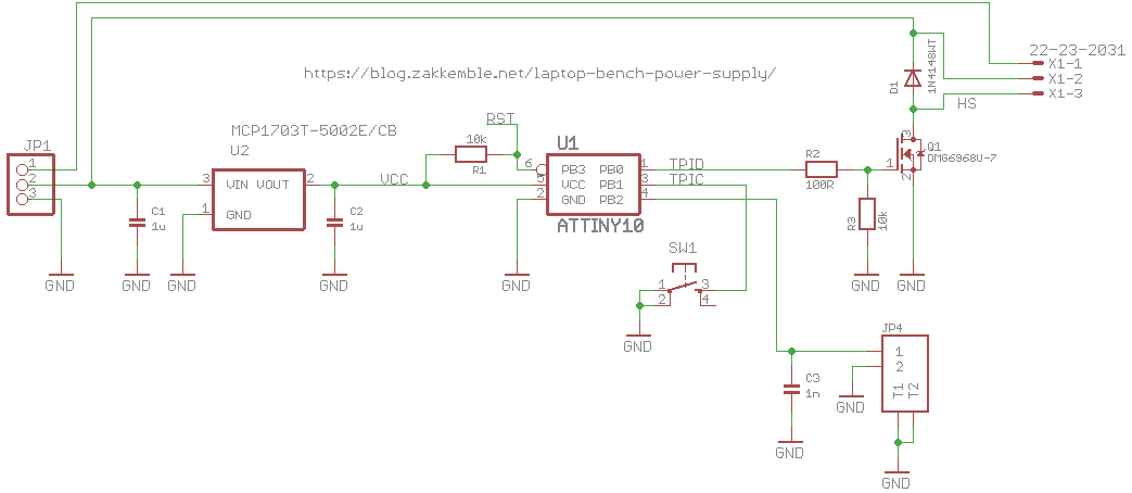
Schematics
As mentioned above, most of the components used are SMD type which means the project is best implemented on a PCB. As such the schematic was designed using Autodesk Eagle CAD. The components are connected as shown in the image below:
To make it easy to connect the Delta EFB0412VHD fan to the PCB, a 1 x 3 header pin was used.
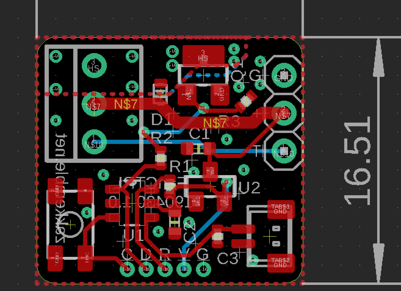
After the schematics design has been done, we then switch to the Eagle Board Layout where the PCB is created. The PCB after routing looks like the image below;
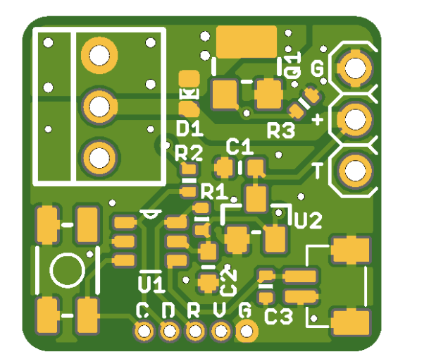
Viewing in 3D to get insight into how things will look after manufacturing:
The schematics and PCB files are provided in a zip file under the download section to make it easy to generate the Gerber files or make any modification you desire on the project.
Preparing the Arduino IDE
While the code for today’s project could have been developed using platforms like Atmel Studio, we will use the Arduino IDE due to it’s popularity and the fact that using it could also teach you a new hack.
Programming the ATtiny10 with the Arduino IDE is a bit different from how the IDE works for other microcontrollers because unlike the SPI protocol used in programming larger AVR chips like the Atmega328p on the Arduino Uno, the ATtiny10 uses a programming protocol called TPI (Tiny Programming Interface) which needs only five wires. As such, it requires modifications in the software and hardware involved.
For software modification, we will need to add the Attiny10 core to the Arduino IDE. While there are a few ATtiny10 cores out there, for this project, we will use the Core developed by Johnson Davies. The core is essentially a boards.txt file that adds options for ATtiny10/9/5/4 to the Arduino IDE’s Board menu so they can be programmed using the Arduino IDE. However, this core doesn’t include the Arduino support core, as a result, it does not support the popular Arduino functions like pinMode(), millis(), etc., so the code must be developed in pure C programming language. To install the ATtiny10 Core, download the core from it’s GitHub page. Extract the zip file, and copy its content to the hardware folder inside the Arduino folder (the same folder where your sketches and Library folder is located) in your Documents folder. If there is no hardware folder, create it before doing any other thing. According to the Github page, the ATtiny10Core should work with all versions of the official Arduino IDE (from arduino.cc) from version 1.6.3 onwards but versions from 1.8.3 and up are recommended.
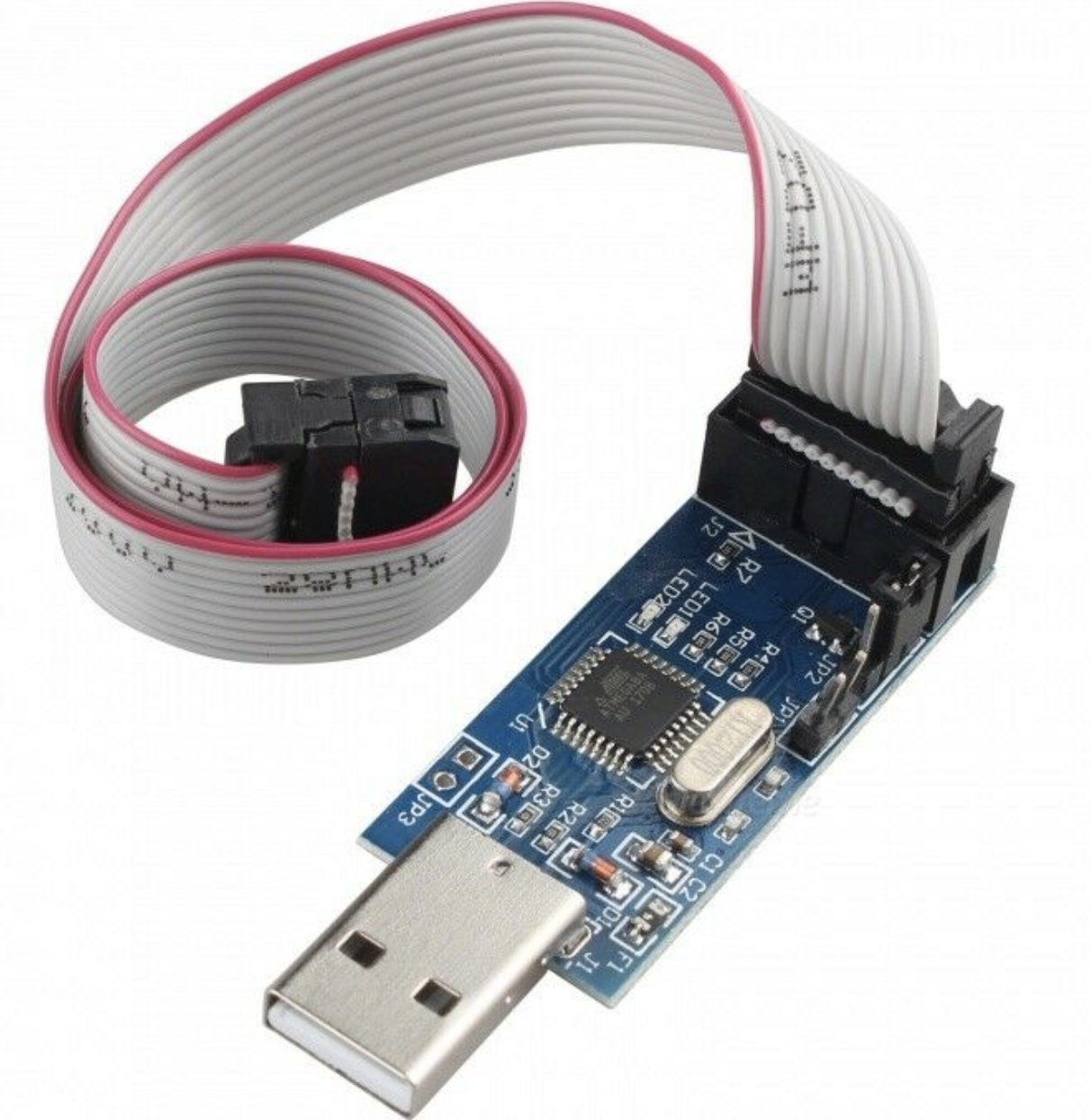
USBasp Programmer
On the hardware side, the popular usb-serial converters cannot be used in programming the ATtiny10 due to the TPI interface requirement but fortunately for us, Thomas Fischl created an excellent USBasp programmer which supports this protocol so you can build your own using his guide or just order one with a 10pin or 6pin adapter for ISP from his website or others like eBay and Banggood.
With all of these in place, we are now ready to write the code for the project.
Code
As mentioned above, the ATtiny10 core being used does not support the Arduino functions so we need to develop the code in pure C/C++. To do this effectively, one needs to understand how the Arduino functions translate in core C/C++ and how ports work. You can check out these explanations to better understand it.
As usual I will do a quick breakdown of the code to explain how each of the parts work.
We start the code by including libraries that allow us use standard AVR register definitions and standard C++ routines.
Next, we create variables to hold the state of the fan, intervals at which the temperature is measured, and temperature threshold at which it is declared HOT or COLD.
#define FAN_OVERRIDE_NONE 0
#define FAN_OVERRIDE_ON 1
#define FAN_OVERRIDE_OFF 2
#define FAN_COOL_TIME 125 // 125 * 64ms = 8s // Keep fan on for this much longer after COOL_VAL has been reached
#define TEMP_MEASURE_INTERVAL 32 // 32 * 64ms = 2s // How often to measure temperature
#define HOT_VAL 23 // Sense: 4k @ ??C
#define COOL_VAL 27
Next, we declare that the state of each of the pin should be and the value that should be associated with that state.
Next, we create the main function. The main function is similar to the void loop() as it contains the code snippets we hope to run perpetually but unlike the Arduino void loop function, it also contains code snippets similar to what we would have written for the void setup() function. The convention used in the Arduino version can however be retained but for this tutorial we will write the standard C version of the main() function.
We start the main() function by setting the clock and declaring the pin mode of the pin on the port that we will be using as 0 (Indicating the PinMode as input). After this we activate the internal pull up resistors using a separate pullup register, PUEB, power off analog comparators, setup the ADC and power off everything else to save power.
int main(void)
{
clock_prescale_set(CPU_DIV);
DDRB |= _BV(DDB0);
PUEB |= _BV(PUEB1);
ACSR = _BV(ACD); // Power off analogue comparator
// Setup ADC
ADMUX = _BV(MUX1);
ADCSRA = _BV(ADIE)|_BV(ADPS2)|_BV(ADPS0);
DIDR0 = _BV(ADC2D);
power_all_disable(); // Power off everything else
Next we initialize variables that will be used to; hold the last temperature to determine if a change has occurred, check if the button is pressed or not, and start the fan in an override mode. With that done, we set the global interrupt flag by calling sei().
uint8_t now = 0;
uint8_t lastMeasureTemp = 0;
uint8_t lastHotTime = (0 - FAN_COOL_TIME) + 31; // Turn fan on for 2 seconds at power on
uint8_t hot = 0;
uint8_t btnIsPressed = 0;
uint8_t fanOverride = FAN_OVERRIDE_NONE;
sei();
Next we handle Watchdog resets and finally write the code that compares the temperature level and turns the fan “ON” or “OFF” depending on it while also checking the pushbuttons in every 64ms to see if the mode of use has changed. Depending on the Mode, the Fan can either be activated or not. If the pushbutton is pressed, the system checks the last state of the fan and switches to an opposite state and continues to run in that opposite state until the push button is pressed again. However, if the button is not pressed the fan runs its on and off duty based on the temperature and time.
sei();
// Was reset by the watchdog (mainly for debugging)
if(rstflr_mirror & _BV(WDRF))
{
while(1)
{
// _delay_ms() is giving some asm error (avr-libc bug? GCC 8.3.0)
for(uint16_t i=0;i<20000;i++)
{
WDT_INT_RESET();
_delay_us(100);
}
//_delay_ms(2000);
FAN_ON();
// _delay_ms() is giving some asm error (avr-libc bug? GCC 8.3.0)
for(uint16_t i=0;i<5000;i++)
{
WDT_INT_RESET();
_delay_us(100);
}
//_delay_ms(500);
FAN_OFF();
}
}
WDT_INT_RESET();
while(1)
{
// Timer stuff, increments every 64ms from the WDT
// Also turns the WDT back on
if(WDT_TIMEDOUT())
{
WDT_INT_RESET();
now++;
}
if((uint8_t)(now - lastMeasureTemp) >= TEMP_MEASURE_INTERVAL)
{
// Pullup enable
PUEB |= _BV(PUEB2);
lastMeasureTemp = now;
// Wait for a bit for voltage to stabilize
// _delay_ms() is giving some asm error (avr-libc bug? GCC 8.3.0)
for(uint8_t i=0;i<10;i++)
_delay_us(100);
//_delay_ms(1);
// Do an ADC convertion
power_adc_enable();
ADCSRA |= _BV(ADEN)|_BV(ADSC);
set_sleep_mode(SLEEP_MODE_ADC);
sleep_mode();
loop_until_bit_is_clear(ADCSRA, ADSC); // In case we wakeup from another interrupt before the convertion completes
uint8_t val = ADCL;
ADCSRA &= ~_BV(ADEN);
power_adc_disable();
// Pullup disable
PUEB &= ~_BV(PUEB2);
if(val > COOL_VAL)
hot = 0;
else if(val < HOT_VAL)
hot = 1;
// else we're between the hot and cool values (hysteresis)
if(hot)
lastHotTime = now;
}
// Don't need to bother with switch debouncing here since we only loop every ~64ms from the WDT
if(BTN_ISPRESSED() && !btnIsPressed)
{
btnIsPressed = 1;
if(fanOverride == FAN_OVERRIDE_NONE)
{
fanOverride = FAN_OVERRIDE_ON;
FAN_ON();
}
else if(fanOverride == FAN_OVERRIDE_ON)
{
fanOverride = FAN_OVERRIDE_OFF;
FAN_OFF();
}
else
{
fanOverride = FAN_OVERRIDE_NONE;
if(!hot)
lastHotTime = now - FAN_COOL_TIME;
}
}
else if(!BTN_ISPRESSED() && btnIsPressed)
btnIsPressed = 0;
if(fanOverride == FAN_OVERRIDE_NONE)
{
if(hot || (uint8_t)(now - lastHotTime) < FAN_COOL_TIME)
FAN_ON();
else
{
FAN_OFF();
lastHotTime = now - FAN_COOL_TIME;
}
}
// Sleep if nothing to do
cli();
if(!WDT_TIMEDOUT())
{
set_sleep_mode(SLEEP_MODE_PWR_DOWN);
sleep_enable();
//sleep_bod_disable();
sei();
sleep_cpu();
sleep_disable();
}
sei();
}
}
EMPTY_INTERRUPT(WDT_vect);
EMPTY_INTERRUPT(ADC_vect);
The complete code for the project is provided below and attached in the zip file under the download section.
#include <stdint.h>
#include <avr/io.h>
#include <avr/power.h>
#include <avr/wdt.h>
#include <avr/interrupt.h>
#include <avr/sleep.h>
#include <util/delay.h>
#define FAN_OVERRIDE_NONE 0
#define FAN_OVERRIDE_ON 1
#define FAN_OVERRIDE_OFF 2
#define FAN_COOL_TIME 125 // 125 * 64ms = 8s // Keep fan on for this much longer after COOL_VAL has been reached
#define TEMP_MEASURE_INTERVAL 32 // 32 * 64ms = 2s // How often to measure temperature
// Temperature sensor resistance is 10k @ 22C
// Sensor resistance goes down as temperature goes up
// Pullup resistance is around 40k
// Lower value = hotter
#define HOT_VAL 23 // Sense: 4k @ ??C
#define COOL_VAL 27
#define WDT_INT_RESET() (WDTCSR |= _BV(WDIE)|_BV(WDE)) // NOTE: Setting WDIE also enables global interrupts
#define WDT_TIMEDOUT() (!(WDTCSR & _BV(WDIE)))
#define FAN_ON() (PORTB |= _BV(PORTB0))
#define FAN_OFF() (PORTB &= ~_BV(PORTB0))
#define BTN_ISPRESSED() (!(PINB & _BV(PINB1)))
// PB0 = Fan out
// PB1 = Switch in
// PB2 = Temp sense ADC
static uint8_t rstflr_mirror __attribute__((section(".noinit,\"aw\",@nobits;"))); // BUG: https://github.com/qmk/qmk_firmware/issues/3657
void get_rstflr(void) __attribute__((naked, used, section(".init3")));
void get_rstflr()
{
rstflr_mirror = RSTFLR;
RSTFLR = 0;
//wdt_disable();
wdt_enable(WDTO_60MS);
}
int main(void)
{
  clock_prescale_set(CPU_DIV);

  DDRB |= _BV(DDB0);
  PUEB |= _BV(PUEB1);

  ACSR = _BV(ACD); // Power off analogue comparator

  // Setup ADC
  ADMUX = _BV(MUX1);
  ADCSRA = _BV(ADIE)|_BV(ADPS2)|_BV(ADPS0);
  DIDR0 = _BV(ADC2D);

  power_all_disable(); // Power off everything else
      uint8_t now = 0;
uint8_t lastMeasureTemp = 0;
uint8_t lastHotTime = (0 - FAN_COOL_TIME) + 31; // Turn fan on for 2 seconds at power on
uint8_t hot = 0;
uint8_t btnIsPressed = 0;
uint8_t fanOverride = FAN_OVERRIDE_NONE;

sei();
// Was reset by the watchdog (mainly for debugging)
if(rstflr_mirror & _BV(WDRF))
{
while(1)
{
// _delay_ms() is giving some asm error (avr-libc bug? GCC 8.3.0)
for(uint16_t i=0;i<20000;i++)
{
WDT_INT_RESET();
_delay_us(100);
}
//_delay_ms(2000);
FAN_ON();
// _delay_ms() is giving some asm error (avr-libc bug? GCC 8.3.0)
for(uint16_t i=0;i<5000;i++)
{
WDT_INT_RESET();
_delay_us(100);
}
//_delay_ms(500);
FAN_OFF();
}
}
WDT_INT_RESET();
while(1)
{
// Timer stuff, increments every 64ms from the WDT
// Also turns the WDT back on
if(WDT_TIMEDOUT())
{
WDT_INT_RESET();
now++;
}
if((uint8_t)(now - lastMeasureTemp) >= TEMP_MEASURE_INTERVAL)
{
// Pullup enable
PUEB |= _BV(PUEB2);
lastMeasureTemp = now;
// Wait for a bit for voltage to stabilize
// _delay_ms() is giving some asm error (avr-libc bug? GCC 8.3.0)
for(uint8_t i=0;i<10;i++)
_delay_us(100);
//_delay_ms(1);
// Do an ADC convertion
power_adc_enable();
ADCSRA |= _BV(ADEN)|_BV(ADSC);
set_sleep_mode(SLEEP_MODE_ADC);
sleep_mode();
loop_until_bit_is_clear(ADCSRA, ADSC); // In case we wakeup from another interrupt before the convertion completes
uint8_t val = ADCL;
ADCSRA &= ~_BV(ADEN);
power_adc_disable();
// Pullup disable
PUEB &= ~_BV(PUEB2);
if(val > COOL_VAL)
hot = 0;
else if(val < HOT_VAL)
hot = 1;
// else we're between the hot and cool values (hysteresis)
if(hot)
lastHotTime = now;
}
// Don't need to bother with switch debouncing here since we only loop every ~64ms from the WDT
if(BTN_ISPRESSED() && !btnIsPressed)
{
btnIsPressed = 1;
if(fanOverride == FAN_OVERRIDE_NONE)
{
fanOverride = FAN_OVERRIDE_ON;
FAN_ON();
}
else if(fanOverride == FAN_OVERRIDE_ON)
{
fanOverride = FAN_OVERRIDE_OFF;
FAN_OFF();
}
else
{
fanOverride = FAN_OVERRIDE_NONE;
if(!hot)
lastHotTime = now - FAN_COOL_TIME;
}
}
else if(!BTN_ISPRESSED() && btnIsPressed)
btnIsPressed = 0;
if(fanOverride == FAN_OVERRIDE_NONE)
{
if(hot || (uint8_t)(now - lastHotTime) < FAN_COOL_TIME)
FAN_ON();
else
{
FAN_OFF();
lastHotTime = now - FAN_COOL_TIME;
}
}
// Sleep if nothing to do
cli();
if(!WDT_TIMEDOUT())
{
set_sleep_mode(SLEEP_MODE_PWR_DOWN);
sleep_enable();
//sleep_bod_disable();
sei();
sleep_cpu();
sleep_disable();
}
sei();
}
}
EMPTY_INTERRUPT(WDT_vect);
EMPTY_INTERRUPT(ADC_vect);
Uploading the Code
With the code verified, PCB soldered, and every other thing in place, follow the steps below to upload the code to the Attiny10.
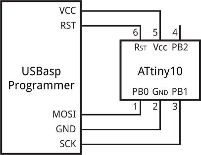
Connect USBasp Programmer to ATtiny10
Connect the USBasp to the ATtiny10 as shown in the diagram above.
Select the board type from the options under the ATtiny10 core board options under the tool menu. Tools->Board -> ATtiny10
Under the programmer option, select USBasp as the programmer. Tools -> Programmer-> USBasp
Hit the upload button
Do note that the code could also be developed using platforms like Atmel Studio and the procedure would have been only a little bit different.
Demo
With the code uploaded, connect/mount the smart fan on one of your projects/devices. As the device gets hot or cold, you should see the fan come on and go off.
To test the project, it was connected it to a Bench Power supply and the overall performance was definitely better than when an ordinary heat sink was used. A picture of Zak’s setup is shown in the image below.
That’s it. The idea of the project was to provide you with a module like unit that can be used to maintain acceptable temperature levels in your project. Feel free to reach out to me via the comment section if you have any issue replicating this.
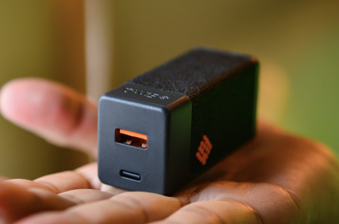
Though the sizes of laptops and mobile phones have become smaller and lighter over the years, that of power adapters have pretty much remained the same. They are still the same device we have always known them to be; bulky, messy and hard-to-carry-around. But the new GaNtechnology seeks to bring a revolution in the world of power electronics.
The new series of SlimQ power adapters made of GaN technology is a new set of smaller and lighter adapters that works for all modern models of laptops and phones that use USB Type-C power supply up to 65W.
The SlimQ 65W power adapter is the world’s first and smallest most-affordable power adapter. It is safe, more powerful and more efficient with a high-quality built to give protection against input and output over current protection, over-voltage, short current, leakage, and electric surge,anti-electromagnetic and anti-ripple effect. The 65W adapter is about 6ft/1.8m in size, elastic, durable, supports Type-C to Type-C and has a current capacity of 3.5A. It also works great with major laptop brands that use non-Type-C for the power supply but comes with a converter cable as a part of the accessories.
The SlimQ 65W power adapter is sold at a retail price of $16 and its hardware and accessories come with a limited one year warranty. Apart from the countries that have been flagged by courier services, the adapters can be shipped to anywhere in the world but come with more cost if you wish to ship to any of those countries. To order the adapter, simply visit the Indiegogo site to select the particular “perk” you’d want to buy. There are quite a number of perks there, so you’d have to swipe right and left to find the particular one you want. Click on payment and proceed to select add-on perks that you will find the cables compatible with your laptop.
The SlimQ is travels-friendly as it comes with a travel bag in which it can be stowed away. It has a default US-style plug but there is a free converter that comes with it for you to use if you are out of the United States. For instance, a UK style converter is included for those in places like UK, Singapore, Hong-Kong and likewise an AU style converter for New Zealand, Australia and an EU converter for those in Italy, France, Germany, Swiss. There are also applicable VAT/GST charges that depend on your country’s regulations. Shipping fees vary among different countries and it is through post service but a different shipping method can be arranged if ordered.
u-blox, a global provider of leading positioning and wireless communication technologies, has announced its new ultra-robust meter-level M9 global positioning technology platform, designed for demanding automotive, telematics, and UAV applications.
Thanks to its high performance GNSS chip, UBX-M9140, the M9 technology platform and the NEO-M9N, the first module based on the platform, can receive signals from up to four GNSS constellations (GPS, Glonass, Beidou, and Galileo) concurrently, in order to achieve high positional accuracy even in difficult conditions such as deep urban canyons. The u-blox M9 offers a position update rate of up to 25 Hz, enabling dynamic applications like UAVs to receive position information with low latency.
The u-blox M9 also features a special filtering against RF interference and jamming, spoofing detection, and advanced detection algorithms that enable it to report fraudulent attacks quickly so that users’ systems can react to them in a timely fashion. A SAW (surface acoustic wave) filter combined with an LNA (low noise amplifier) in the RF path is integrated in the NEO-M9N module. This setup guarantees normal operations even under strong RF interferences, for example when a cellular modem is co-located with the NEO-M9N.
“We’ve developed the u-blox M9 as a follow-on from our very successful u-blox M8 GNSS platform, offering even more robust meter-level positioning technology and security features to protect the integrity of applications in the automotive, telematics, and UAV markets,” says Bernd Heidtmann, Product Manager, Product Strategy GNSS, Product Center Positioning, at u-blox.
Users of the u-blox M9 will therefore benefit from it being part of the wider u-blox product family, which means that developers will be able to design a single PCB and then migrate to a different positioning technology, such as dead reckoning augmenting GNSS technology, with very little change to the board design.
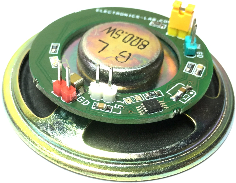
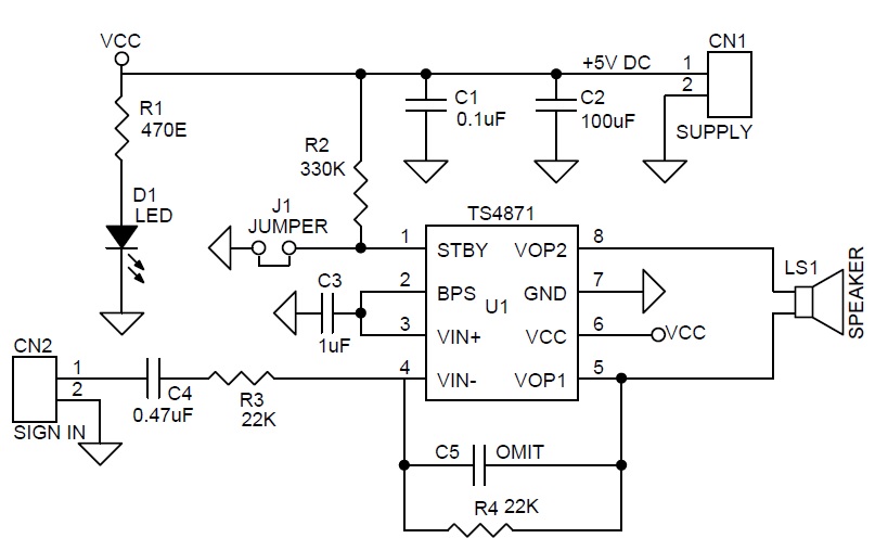
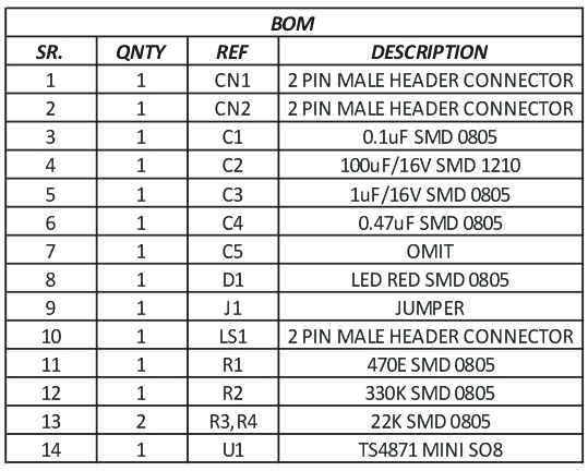
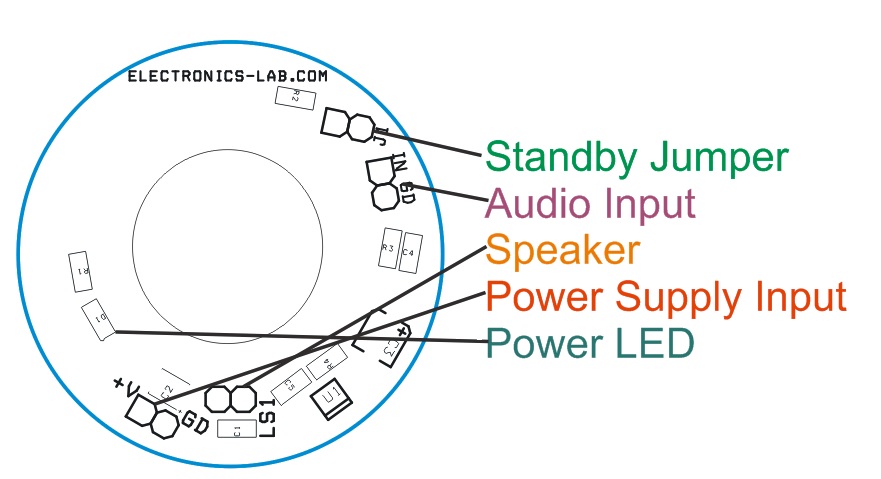
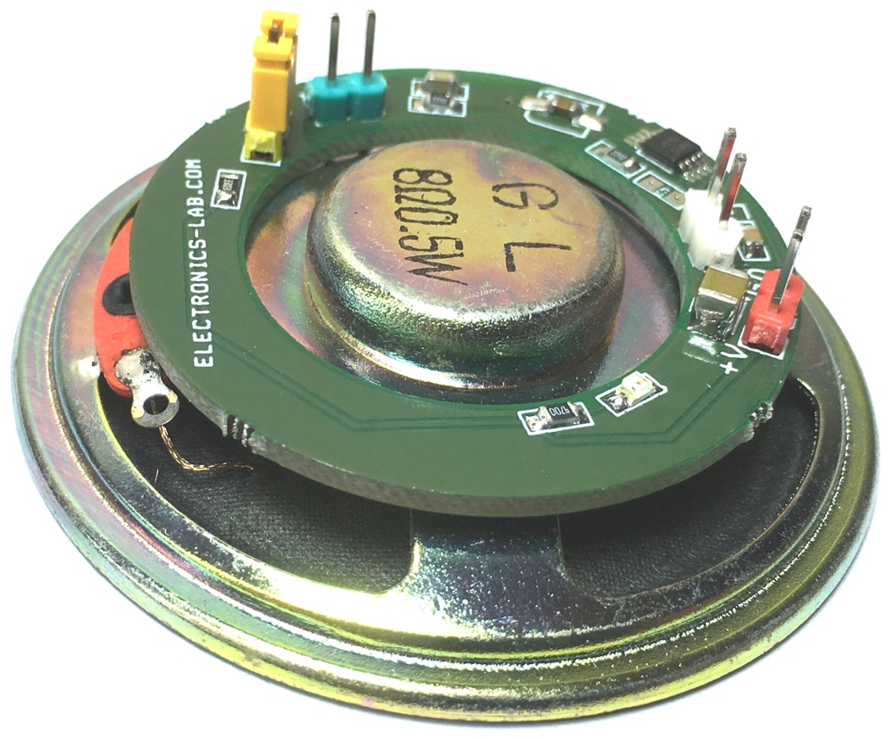
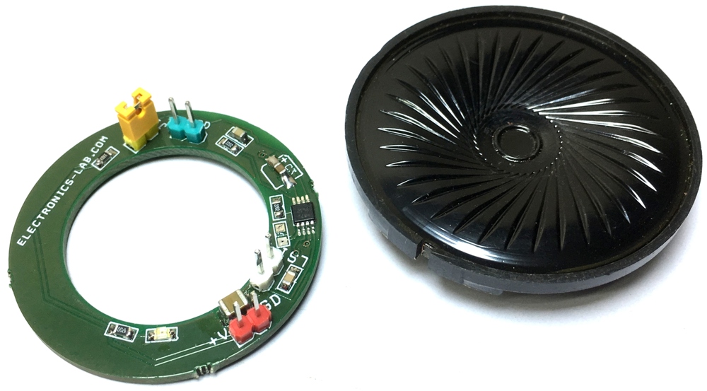
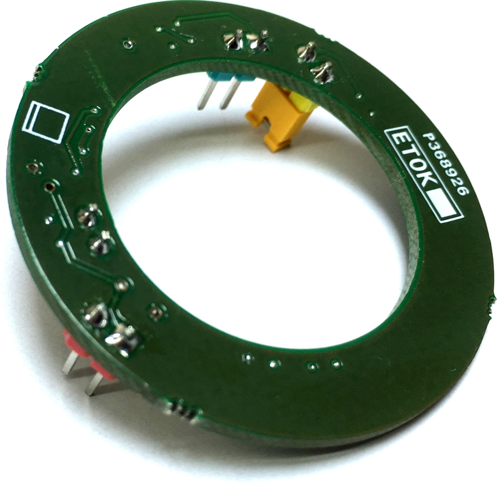
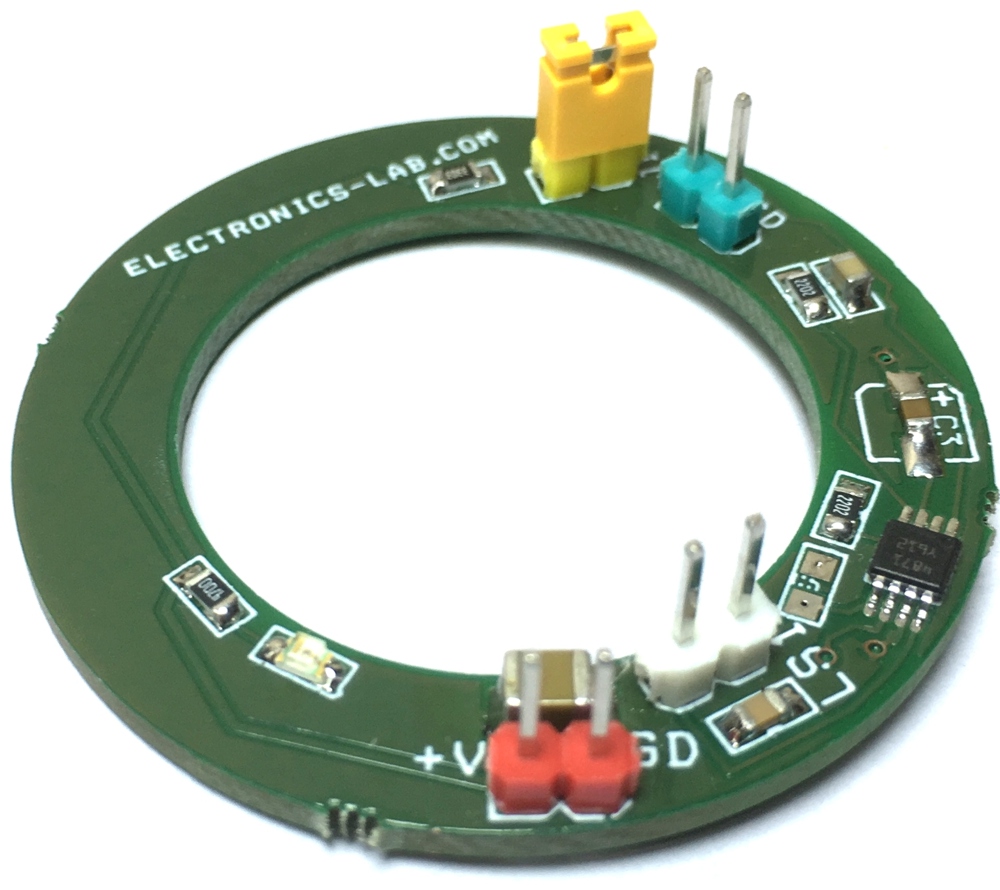
This Mini Audio Power Amplifier is capable of delivering 1W of continuous RMS Output Power into 8 ohms load @ 5V. The Amplifier is built using TS4871 IC from ST. This Audio Amplifier is exhibiting 0.1% distortion level (THD) from a 5V supply for a Pout = 250mW RMS. An external standby mode control reduces the supply current to less than 10nA. An internal thermal shutdown protection is also provided. The amplifier has been designed for high quality audio applications such as mobile phones, media players and portable device. The gain is set to 6dB but unity-gain stable amplifier can be configured by external gain setting resistor R4. 28mm ID hole provided for easy mounted of PCB directly on speaker.
Mini Speaker Attached Audio Amplifier using TS4871 – [Link]
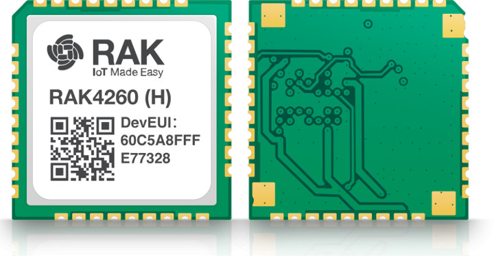
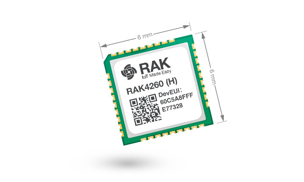
Rakwireless has just announced a new module part of their LPWAN family: RAK4260 LoRaWAN module based on Microchip ATSAMR34J18B LoRa SiP and at just 15x15x1.2 mm, one of the smallest LoRaWAN modules in the market.
The new module is cheaper than the company’s earlier RAK811 module and consumes less power at just 790 nA in sleep mode. The company also provides a RAK4260 evaluation board with easy access to GPIOs and serial interfaces.
Key Specifications:
High quality Low power LoRa® device (Microchip ATSAMR34J18 SiP)
Fully supported 862 to 1020 MHz frequency coverage (all LoRaWAN bands)
High level of accuracy and stability (32MHz TXCO)
Max Tx Power: 20dBm; Max Sensitivity: -148dBm; Rx Current: 17mA (typical)
Rich selection of interfaces: I2C, SPI, ADC, UART, GPIOs
Small form factor: 6×6 mm compact BGA package
Specifications:
SiP – Microchip ATSAMR34J18 SiP with SAM L21 Arm Cortex M0+ MCU @ 48 MHz, up to 40 KB RAM, up to 256 KB Flash
LoRa Connectivity
Frequency Range – 862 to 1020 MHz
High level of accuracy and stability (32MHz TXCO)
Max Tx Power: 20dBm; Max Sensitivity: -148dBm; Rx Current: 17mA (typical)
Compliant with LoRaWan 1.0.2
Expansion – Castellated holes with I2C, SPI, ADC, UART, GPIOs
Power Consumption
Low RX current of 13.6mA
790 nA in sleep mode
Dimensions – 15×15 mm
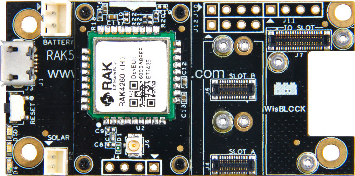
RAK4260 Evaluation Board
The evaluation board is based on RAK5005 carrier board and RAK4261 intermediate board which has RAK4260 soldered to it.
There aren’t any details about the board by we can see three power options with micro USB port, 2-pin battery header, and 2-pin solar panel header. There are various expansion headers as well as and connectors for Wisblock add-on modules.
Documentation and Software
Documentation is still work in progress, but you’ll find a getting started guide on the documentation page explaining how to flash the firmware, and configure the board with The Things Network (TTN). The demo firmware is based on Microchip SDK, and you’ll find the source code on Github.
Availability and Pricing
Both the module and evaluation board are available on Aliexpress, with a pack of 50 modules selling for $440 (or $8.80 per unit), and the EVB4260 EVB going for $25 plus shipping.
More information may eventually be available on the product page.
This Mini Audio Power Amplifier is capable of delivering 1W of continuous RMS Output Power into 8 ohms load @ 5V. The Amplifier is built using TS4871 IC from ST. This Audio Amplifier is exhibiting 0.1% distortion level (THD) from a 5V supply for a Pout = 250mW RMS. An external standby mode control reduces the supply current to less than 10nA. An internal thermal shutdown protection is also provided. The amplifier has been designed for high quality audio applications such as mobile phones, media players and portable device. The gain is set to 6dB but unity-gain stable amplifier can be configured by external gain setting resistor R4. 28mm ID hole provided for easy mounted of PCB directly on speaker.
Connections: D1 Power LED, CN1 Power input, LS1 Speaker, CN2 Audio Signal Input.
Note : Default Gain 6dB, Change R4 to 110K to set the Gain to 20dB.
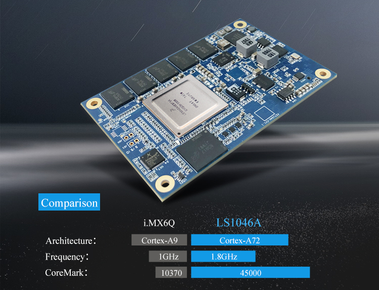
NXP LS1043A quad-core Cortex-A53 communication processor was introduced in 2014, while NXP LS1046A quad-core Cortex-A72 SoC was launched about 18 months later. Both are designed for networking equipment such as CPE (Customer Premise Equipment), routers, NAS, gateways, as well as single board computers and include one or two 10 GbE interfaces.
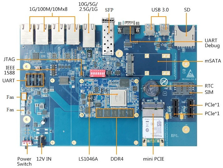
Forlinx Embedded has decided to leverage those two processors in their OK1043A-C and OK1046A industrial-grade single board computers designed for networking applications.
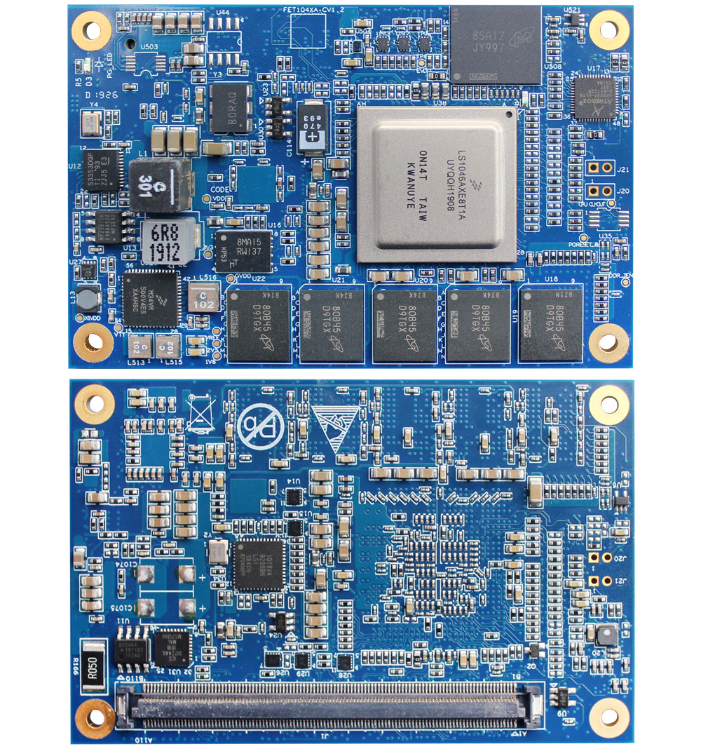
Both boards are comprised of the same baseboard and only differ by their COM-Express Mini Type 10 module which comes with the processor, memory, and flash storage.
Specifications:
COM Express Mini System-on-Module (one or the other)
FET1046A-C NXP LS1046A SoM
CPU – NXP LS1046A quad-core Cortex-A72 processor @ up to 1.8GHz
System Memory – 2GB DDR4 RAM
Storage – 8GB eMMC flash + 16MB QSPI NOR Flash
Voltage Input – 12V
Temperature Range – -40℃ to +75℃
Dimensions – 84 x 55mm
FET1043A-C LS1043A SoM
CPU – NXP LS1043A quad-core Cortex-A53 @ up to 1 .6GHz
System Memory – 2GB DDR4
Storage – 8GB eMMC flash + 16MB QSPI NOR Flash
Voltage Input – 12V
Temperature Range – -40℃ to +80℃
Dimensions – 84x 55mm
Carrier Board
Storage
SD card socket multiplexed with eMMC, bootable
1x mSATA 3.0 up to 6Gbps
Networking
Up to 6x 6 Gigabit Ethernet ports (4x from QSGMII and 2x from RGMII)
1x 10Gbps Ethernet port (RJ45)
LS1046A only – 1x 10 Gbps Ethernet Port (SFP+) for optical module or SFP-GE transceiver
USB – 2x USB 3.0 ports
Expansion
1x Mini PCIe 2.0 up to 5GT/s with USB and SIM card signals for 4G module; SIM card slot
2x PCIe 2.0 up to 5GT/s
3x UART TLL headers
Debugging – 1x RS232 debug port, JTAG header with support for NXP CodeWarrior TAP
Misc – RTC with on-board CR2032 cell, fan headers, configuration dip-switch, power switch
Power Supply – 12V via power barrel jack
Dimensions – TBD
So the main difference is that LS1043A can support up to 7 Ethernet ports (1x XFI 10Gbps Ethernet + 6x Gigabit Ethernet), while LS1046A can handle up to 8 Ethernet ports (2x XFI 10Gbps Ethernet + 6x Gigabit Ethernet).
Both boards run Ubuntu 18.04 with Linux 4.14.4 or OpenWrt 17.01 with Linux 4.14.69 , and the company provides complete BSP with source code to their customers (no public download).
Target applications include industrial routers, edge computing gateways, IP-PBX, energy management, automation, and more. Both boards and corresponding modules appear to be available now at an undisclosed price. You may find more details about OK1043A-C and OK1046A-C networking SBCs on the respective product pages here and there.
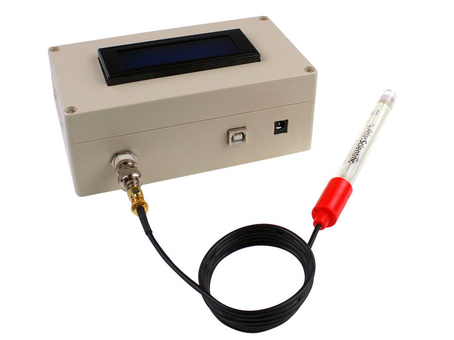
pH meters are scientific instruments used for measuring the activity and concentration of hydrogen-ions in water-based solutions, with the aim of indicating its acidity or alkalinity expressed as pH values. They find application in water & wastewater treatment, pharmaceuticals, chemicals & petrochemicals, food & beverages, mining, and agricultural processes to mention a few. For today’s tutorial, we will attempt to build an accurate, DIY version of this very useful tool.
DIY pH Meter
pH meters comprises of majorly a probe and a processing unit which interprets the data from the probe and displays in a human readable format. pHmeter essentially measures the difference in electrical potential between a pH electrode and a reference electrode. As a result of this, pH meters are sometimes referred to as a “potentiometric pH meters”.
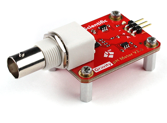
Gravity analog pH meter breakout board
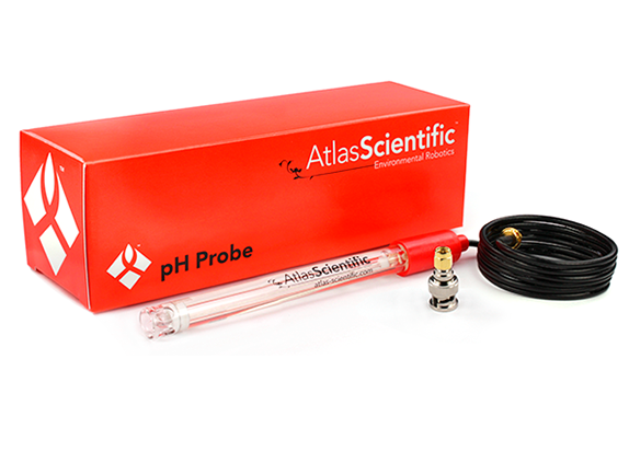
While there are several DIY pHmeter examples on the internet, today’s project will be based on the examples provided by Atlas Scientific. We will use the Atlas Scientific pH probe and their Gravity analog pH meter breakout board. The Gravity analog pH meter breakout board is a fairly accurate low-cost pH metering solution specifically designed for Students / education, Proof of concept developments and pH metering applications requiring moderate accuracy levels. It comes with a BNC port through which it can be connected to the Atlas Scientific pH probe.
Atlas Scientific pH probe
Asides the pH breakout and the probe, we will use an Arduino Uno and a 20×4 LCD display. The Arduino will serve as the brain for the project obtaining the pH level from the probe while the LCD will serve the purpose of providing visual feedback to the users as the value obtained by the Arduino will be displayed on the LCD.
To make the project neat, Atlas Scientific also created a nice enclosure and we will follow the steps outlined by them to create our own.
Ready? let’s jump in.
Required Components
We start by first getting supplies for our build. The following components are needed to build this project;
11mm standoffs and screws (comes with the pH sensor) x4
Resistors 220Ω $ 1kΩ
To reduce the workload associated with searching for the exact components used for this tutorial, I have included links through which each of the components can be bought.
Asides the components, a few tools are required for developing the enclosure, but since that is not so important we will leave it till we get to that stage.
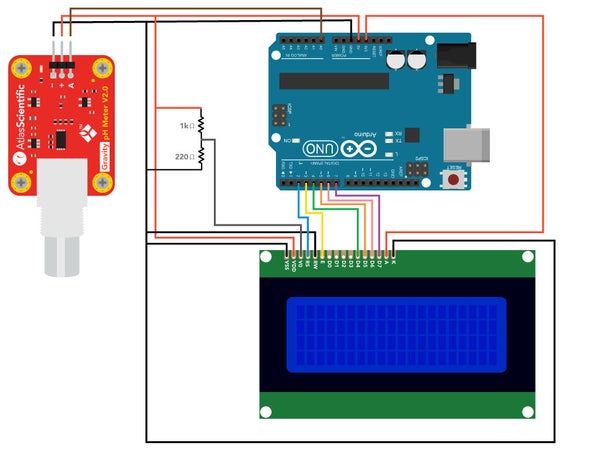
Schematics
The schematics for today’s project is quite straightforward. We will connect the LCD using the 4-pin mode, while we willconnect the signal pin from the PH sensor to an analog pin on the Arduino since it’s output is analog.
Connect the components as shown in the schematics below:
Schematics
To make the schematics easy to follow, a pin map showing how the components are connected to the Arduino is provided below;
PHmeter – Arduino
+/VCC - 5V
-/GND - GND
A/OUT - A0
LCD – Arduino
K - GND
A - 3.3V
D7 - D7
D6 - D6
D5 - D5
D4 - D4
E - D3
RS - D2
R/W - GND
VSS - GND
VDD - 5V
VO - 5V Via Resistors as voltage dividers
Go over the connections when done to ensure everything is as it should be.
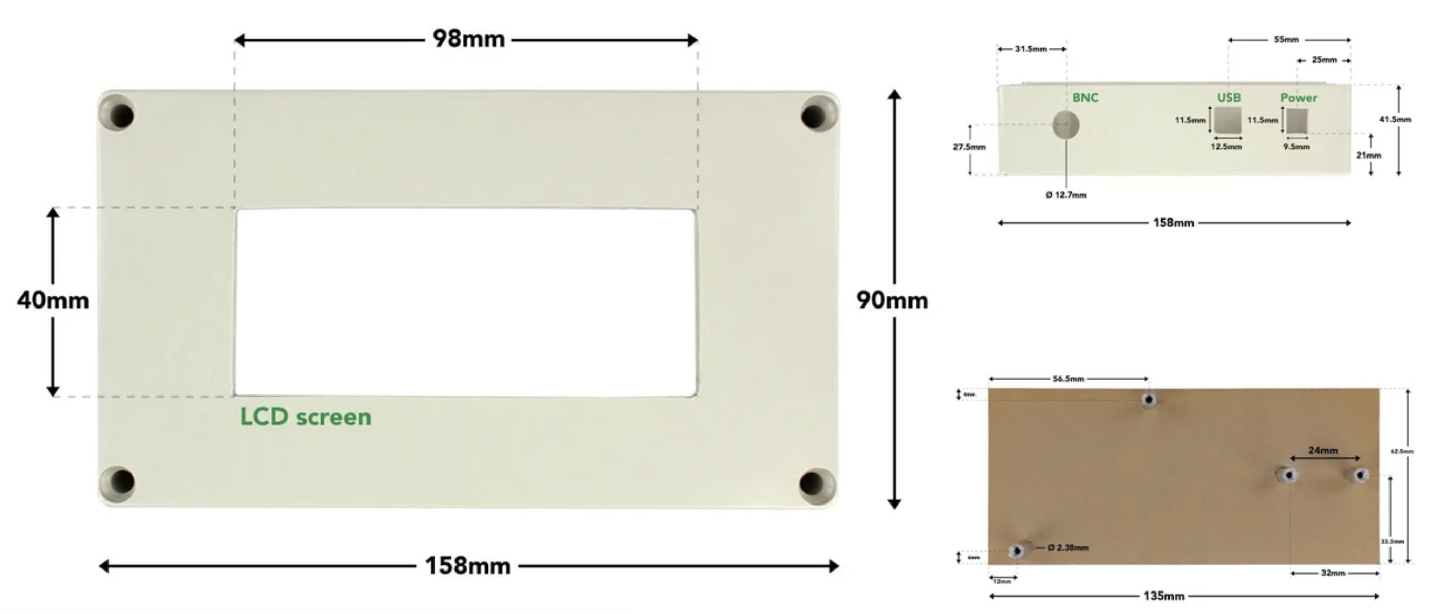
Enclosure Design
With the connections ready, to make the project neat and presentable an enclosure was created. The enclosure is based on the popular abs plastic enclosures and it was modified with drills and other tools so it accommodates the screen and fits perfectly for other projects. A picture of the completed enclosure is displayed in the image below.
DIY pH Meter
To modify the ABS enclosure for the desired neat and clear shape as shown in the picture above, different kind of tools were used including; a Drill, drill bits, drywall cutter bits, files, screwdrivers, benchtop vise, band saw, glue gun and glue stick, soldering iron and solder, digital caliper, ruler. While having these tools makes the process of making the enclosure easier and faster, feel free to use make shift tools that in one way or the other, help achieve the goal of a neat enclosure.
All of the modifications made to the ABS enclosure are based on the diagram below. You may need to zoom in to see the dimensions properly.
You can follow the steps below to achieve this with good precision. Feel free to use other tools/makeshift tools where needed.
Cut opening for the LCD
The LCD is placed in the top portion (cover) of the enclosure. Center a 98x40mm rectangle on the cover.
Put the piece in the vise and drill a 3.2mm (1/8″) pilot hole in the rectangle that was marked off.
Use this pilot hole as the start point for the 3.2mm (1/8″) drywall cutting bit. Since this a small job, we will use the bit on the hand drill rather than a drywall cutting machine. Work on the inside of the rectangle instead of the lines as it may be a bit difficult to cut in a straight manner with this bit on the drill.
Next, use a hand file to remove the excess material and shape the rectangle to the required size.
Cut openings for BNC connector and Arduino ports
The openings for the BNC connector and Arduino ports are on the side of the bottom portion of the enclosure.
Using the dimensions provided above, mark the center point for the circle and outlines for the two rectangles.
Put the piece in the vice and cut the openings. The circular opening is made using drill bits. The rectangular ones are made by following a similar process used to make the opening for the LCD.
Outfit the base plate to mount components
The base plate is used to mount the Arduino, pH sensor and mini breadboard. 6.4mm (1/4″) thick acrylic sheet is used.
Using a band saw, cut the acrylic sheet to 135×62.5mm.
Mark off the positions for the four holes as shown. Drill 2.38mm (3/32″) diameter holes. Countersink the holes on one side of the plate to a depth of 3mm and diameter of 4.4mm (11/64″). This is necessary to keep a flat undersurface when the screws are inserted to hold the standoffs.
Attach the 11mm standoffs using the provided screws. The pH sensor comes with 4 standoffs and screws. Use two of them for the Arduino.
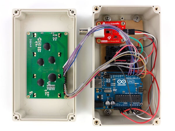
With the enclosure complete, arrange the components inside it such that the set up looks like the image below.
Assembling the components in the Enclosure
Code
The code for today’s project is quite straightforward. Our tasks as mentioned during the introduction is to collect the pH level using the pH meter and display on the attached LCD.
We will use the Arduino IDE for the development of the code and will use 2 major libraries; the Liquid Crystal Display library and the Atlas gravity sensor library. The liquid crystal display library is used to reduce the amount of work/code that is required to get the Arduino to interact with the LCD, while the Atlas Gravity Sensor Library makes it easy to interface with the PH meter and obtain data. The Liquid Crystal Library usually comes with the Arduino IDE but just in case it didn’t, you can always install it via the Arduino Library manager. The Atlas Gravity Sensor library, on the other hand, needs to be installed manually, as such, you will need to download it from the attached link, unzip it and copy it’s content into the Arduino Library folder. The library folder is usually in the same folder as your Arduino Sketches.
With the libraries installed, we can now proceed to writing the code.
The sketch starts by including the libraries that will be used.
#include "ph_grav.h"                                  //header file for Atlas Scientific gravity pHsensor
#include "LiquidCrystal.h"                            //header file for liquid crystal display (lcd)
Next, we declare some of the variables that will be used during the code, declare the analog pin of the Arduino to which the PH sensor analog output pin is connected, and create instances of both the Atlas Gravity Sensor Library and the Liquid Crystal Library.
String inputstring = "";                              //a string to hold incoming data from the PC
boolean input_string_complete = false;                //a flag to indicate have we received all the data from the PC
char inputstring_array[10];                           //a char array needed for string parsing
Gravity_pH pH = A0;                                   //assign analog pin A0 of Arduino to class Gravity_pH. connect output of pH sensor to pin A0
LiquidCrystal pH_lcd(2, 3, 4, 5, 6, 7);               //make a variable pH_lcd and assign arduino digital pins to lcd pins (2 -> RS, 3 -> E, 4 to 7 -> D4 to D7)
With those done, we proceed to to the void setup() function. We start the function by initializing serial communication which will is used for debug purposes, and the LCD display on which a splash/initialization screen is displayed.
void setup() {
  Serial.begin(9600);                                 //enable serial port
  pH_lcd.begin(20, 4);                                //start lcd interface and define lcd size (20 columns and 4 rows)
  pH_lcd.setCursor(0,0);                              //place cursor on screen at column 1, row 1
  pH_lcd.print("--------------------");               //display characters
  pH_lcd.setCursor(0,3);                              //place cursor on screen at column 1, row 4
  pH_lcd.print("--------------------");               //display characters
  pH_lcd.setCursor(5, 1);                             //place cursor on screen at column 6, row 2
  pH_lcd.print("pH Reading");                         //display "pH Reading"
lastly the PH meter is initialized and the control commands for calibration are displayed on the serial monitor.
if (pH.begin()) { Serial.println("Loaded EEPROM");}
  Serial.println(F("Use commands \"CAL,4\", \"CAL,7\", and \"CAL,10\" to calibrate the circuit to those respective values"));
  Serial.println(F("Use command \"CAL,CLEAR\" to clear the calibration"));
 }
Up next is the void loop() function.
The void loop function is quite straight forward. We start by checking if any calibration parameter has been received over the serial monitor. If yes, the data is parsed as an argument into the parse_cmd function where it is used to set the level of calibration required.
void loop() {

  if (input_string_complete == true) {                //check if data received
    inputstring.toCharArray(inputstring_array, 30);   //convert the string to a char array
    parse_cmd(inputstring_array);                     //send data to pars_cmd function
    input_string_complete = false;                    //reset the flag used to tell if we have received a completed string from the PC
    inputstring = "";                                 //clear the string
  }
Next, the PH level is obtained from the PHmeter using the ph.read_ph() function. The values obtained is then displayed on the serial monitor and on the LCD.
  Serial.println(pH.read_ph());                       //output pH reading to serial monitor
  pH_lcd.setCursor(8, 2);                             //place cursor on screen at column 9, row 3
  pH_lcd.print(pH.read_ph());                         //output pH to lcd
  delay(1000);
}
Other parts of the code are the serialEvent() function which is used to obtain user input from the Serial Monitor, and the parse_cmd() function which takes in the data from the serial port and uses it to set the calibration level of the PHmeter.
void serialEvent() {                                  //if the hardware serial port_0 receives a char
  inputstring = Serial.readStringUntil(13);           //read the string until we see a <CR>
  input_string_complete = true;                       //set the flag used to tell if we have received a completed string from the PC
}

void parse_cmd(char* string) {                      //For calling calibration functions
  strupr(string);                                   //convert input string to uppercase

  if (strcmp(string, "CAL,4") == 0) {               //compare user input string with CAL,4 and if they match, proceed
    pH.cal_low();                                   //call function for low point calibration
    Serial.println("LOW CALIBRATED");
  }
  else if (strcmp(string, "CAL,7") == 0) {          //compare user input string with CAL,7 and if they match, proceed
    pH.cal_mid();                                   //call function for midpoint calibration
    Serial.println("MID CALIBRATED");
  }
  else if (strcmp(string, "CAL,10") == 0) {         //compare user input string with CAL,10 and if they match, proceed
    pH.cal_high();                                  //call function for highpoint calibration
    Serial.println("HIGH CALIBRATED");
  }
  else if (strcmp(string, "CAL,CLEAR") == 0) {      //compare user input string with CAL,CLEAR and if they match, proceed
    pH.cal_clear();                                 //call function for clearing calibration
    Serial.println("CALIBRATION CLEARED");
  }
}
The complete code for the project is provided below and also attached under the download section.
/*
Once uploaded, open the serial monitor, set the baud rate to 9600 and append "Carriage return"
The code allows the user to observe real time pH readings as well as calibrate the sensor.
One, two or three-point calibration can be done.

Calibration commands:
 low-point: "cal,4"
 mid-point: "cal,7"
 high-point: "cal,10"
 clear calibration: "cal,clear"
*/

#include "ph_grav.h"                                  //header file for Atlas Scientific gravity pH sensor
#include "LiquidCrystal.h"                            //header file for liquid crystal display (lcd)

String inputstring = "";                              //a string to hold incoming data from the PC
boolean input_string_complete = false;                //a flag to indicate have we received all the data from the PC
char inputstring_array[10];                           //a char array needed for string parsing
Gravity_pH pH = A0;                                   //assign analog pin A0 of Arduino to class Gravity_pH. connect output of pH sensor to pin A0
LiquidCrystal pH_lcd(2, 3, 4, 5, 6, 7);               //make a variable pH_lcd and assign arduino digital pins to lcd pins (2 -> RS, 3 -> E, 4 to 7 -> D4 to D7)


void setup() {
  Serial.begin(9600);                                 //enable serial port
  pH_lcd.begin(20, 4);                                //start lcd interface and define lcd size (20 columns and 4 rows)
  pH_lcd.setCursor(0,0);                              //place cursor on screen at column 1, row 1
  pH_lcd.print("--------------------");               //display characters
  pH_lcd.setCursor(0,3);                              //place cursor on screen at column 1, row 4
  pH_lcd.print("--------------------");               //display characters
  pH_lcd.setCursor(5, 1);                             //place cursor on screen at column 6, row 2
  pH_lcd.print("pH Reading");                         //display "pH Reading"
  if (pH.begin()) { Serial.println("Loaded EEPROM");}
  Serial.println(F("Use commands \"CAL,4\", \"CAL,7\", and \"CAL,10\" to calibrate the circuit to those respective values"));
  Serial.println(F("Use command \"CAL,CLEAR\" to clear the calibration"));
 }


void loop() {

  if (input_string_complete == true) {                //check if data received
    inputstring.toCharArray(inputstring_array, 30);   //convert the string to a char array
    parse_cmd(inputstring_array);                     //send data to pars_cmd function
    input_string_complete = false;                    //reset the flag used to tell if we have received a completed string from the PC
    inputstring = "";                                 //clear the string
  }
  Serial.println(pH.read_ph());                       //output pH reading to serial monitor
  pH_lcd.setCursor(8, 2);                             //place cursor on screen at column 9, row 3
  pH_lcd.print(pH.read_ph());                         //output pH to lcd
  delay(1000);
}

void serialEvent() {                                  //if the hardware serial port_0 receives a char
  inputstring = Serial.readStringUntil(13);           //read the string until we see a <CR>
  input_string_complete = true;                       //set the flag used to tell if we have received a completed string from the PC
}

void parse_cmd(char* string) {                      //For calling calibration functions
  strupr(string);                                   //convert input string to uppercase

  if (strcmp(string, "CAL,4") == 0) {               //compare user input string with CAL,4 and if they match, proceed
    pH.cal_low();                                   //call function for low point calibration
    Serial.println("LOW CALIBRATED");
  }
  else if (strcmp(string, "CAL,7") == 0) {          //compare user input string with CAL,7 and if they match, proceed
    pH.cal_mid();                                   //call function for midpoint calibration
    Serial.println("MID CALIBRATED");
  }
  else if (strcmp(string, "CAL,10") == 0) {         //compare user input string with CAL,10 and if they match, proceed
    pH.cal_high();                                  //call function for highpoint calibration
    Serial.println("HIGH CALIBRATED");
  }
  else if (strcmp(string, "CAL,CLEAR") == 0) {      //compare user input string with CAL,CLEAR and if they match, proceed
    pH.cal_clear();                                 //call function for clearing calibration
    Serial.println("CALIBRATION CLEARED");
  }
}
Calibration
To ensure the accuracy of the results from the pH meter, there is a need to accurately calibrate the device. pH meters are calibrated across 3 levels; 4, 7, and 10 using standard buffer solutions that already exists at that PH level. These standard solutions are sometimes provided by the sellers of the PH sensor but when not provided, you can always get them from your local chemical stores.
To calibrate the meter, upload the sketch we developed above to your Arduino. Take some time to ensure the components are properly connected before doing this. When sketch upload is complete, open the serial monitor, based on our code the serial monitor will prompt you to enter the calibration values, with samples showing how to enter them correctly. When at this stage, follow the steps below to calibrate the meter with the three buffer solutions.
Remove the soaker bottle and rinse the pH probe
Start with the standard buffer solution for pH4. Pour some of the pH 4 solution, enough to cover the probe, into a cup.
Place the probe in the cup and stir it around to remove trapped air. Observe the readings on the serial monitor and leave the probe there till the readings stabilize.
When the readings become stable, enter the command cal,4 into the serial monitor to instruct it to save that value as the calibration value for pH4.
Repeat these steps with the pH7 and pH10 solutions, ensuring you rinse the probe as you move from one solution to the other.
With these done, the pH meter is now calibrated and should be able to give the correct pH level for any solution the probe is tested with. The calibration values are saved on the Arduino’s EEPROM so they are not lost when the meter is disconnected from power. This makes calibration not necessary before every use but you should re-caliberate the system again after some time, so you can always enter the cal,clear command on the serial monitor to clear the previous stored calibration values and repeat the steps explained above.
Demo
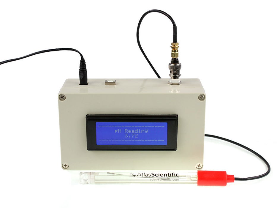
With the code uploaded and calibration done, you can now go ahead and dip the probe into any solution you desire and you should see the pH value displayed on the LCD like shown in the image below.
The accuracy of the pHmeter varies with temperature, as such, it is important to note that the sensor used in this project has an accuracy of +/- 0.2% and that the pH meter will operate at this accuracy level when the temperature range is between 7 – 46°C. Outside of this range, the meter will have to be modified to compensate.
Going forward, while the scope of this project is limited to pH value, you can choose to add several other sensors to make the project more useful. A good example of sensors that could be added for more value include temperature and humidity sensors.
That’s it for this tutorial, thanks for reading. Is there something I missed out, or you have one issue or the other implementing the project? feel free to reach out to me via the comment section.
In the previous tutorials, an important link has been established between the conduction angle of an amplifier and it’s efficiency. Indeed, high conduction angles-based amplifiers offer a very good linearity such as the class A Amplifiers but present a very limited efficiency, generally around 20 to 30 %. As the conduction angle is decreased, high efficiencies are reached such as with the class C amplifiers.
A conduction angle that tends to 0° is therefore desirable to achieve 100 % of efficiency. However, as we have seen with the class C amplifiers, this cannot be implemented since no power is delivered to the load.
Class D amplifiers precisely solve this problem by functioning with a different method than traditional classes A, B, AB or C amplifiers. In the first section, the simplified architecture of a class D amplifiers along with its general functioning are presented. As we will see during this section, class D amplifiers are composed of three different main modules. The next sections are therefore focused on each of these modules to understand how the signal is transformed during the class D amplification process. A little note about the efficiency of this amplifier is given in the last section. Finally, this information is synthesized in a conclusion that summarizes the global transformation of the signal.
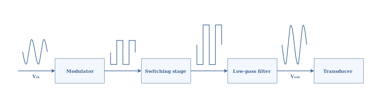
Presentation of the Class D amplification
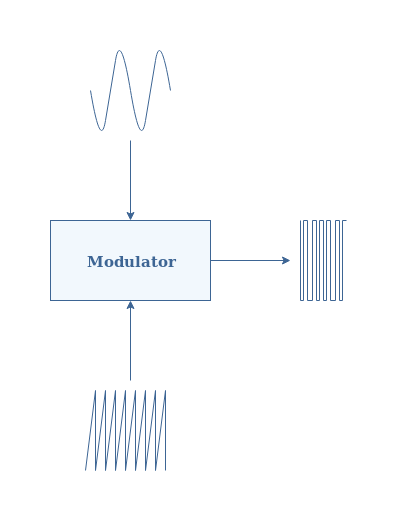
Class D amplifiers generally consists of three different modules : a modulator, a switching stage and a low-pass filter. The signal path along with the succession of these different modules is presented in Figure 1 below :
fig 1 : Flowchart of a class D amplifier
While classic amplifiers accept as an input a sinusoidal signal, Class D amplifiers previously transform it through a modulator into a rectangular signal. We will see in the dedicated section that the view proposed in Figure 1 concerning the modulation is oversimplified.
The switching stage is where the amplification takes places thanks to transistors. We present in detail in the section dealing with this stage that the transistors work in a particular regime and a complementary configuration in order to amplify correctly the rectangle signal.
Finally, a low-pass filter is used in order to restore the sinusoidal shape of the signal. Moreover, this final stage eliminates undesirable harmonics than may have been generated during the amplification process.
Modulation
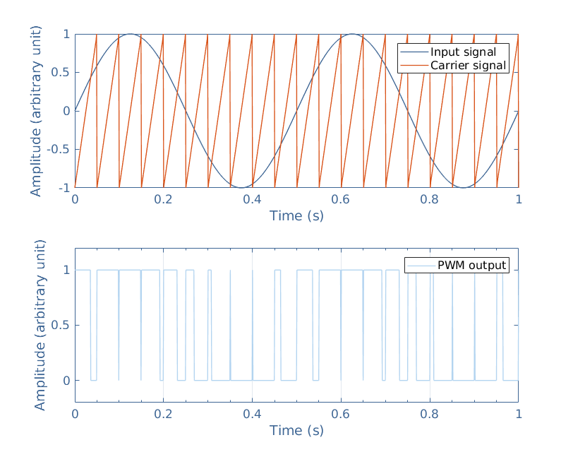
Many modulations techniques exist, however the most common and widely used for many applications is the Pulse Width Modulation (PWM). A simple graph representing the PWM is shown in Figure 2 below :
fig 2 : Principle of a PWM modulator
This technique consists in comparing the input sinusoidal signal with a high frequency triangular signal commonly called carrier obtained from an independent generator. In order to be consistent with Shannon’s theorem, the frequency of the carrier signal must be at least twice as high as the sinusoidal signal frequency.
The output of the modulator is obtained by doing the following comparison between these two signals :
If the sine is above the carrier signal, the output is equal to 1
Otherwise, the output is equal to 0
During the course of this tutorial, the transformation of the signal will be tracked by plotting every step of the amplification with the MatLab® software. In the Figure 3 below, an input signal of frequency 2 Hz is plotted along with a carrier signal of frequency 20 Hz. Moreover, the PWM output is plotted by doing the comparison explained previously.
fig 3 : PWM input and output. Plotted with MatLab®
It is important to note that the frequency of the PWM output is the same as the carrier frequency. The duty cycle is the number characterizing the proportion where the signal value is 1 during a period. For example, if the pulse is symmetrical, half of the signal will be 1 and half 0, the duty cycle is therefore 50 % or 0.5. In the case of a PWM, while the frequency is constant, the duty cycle varies.
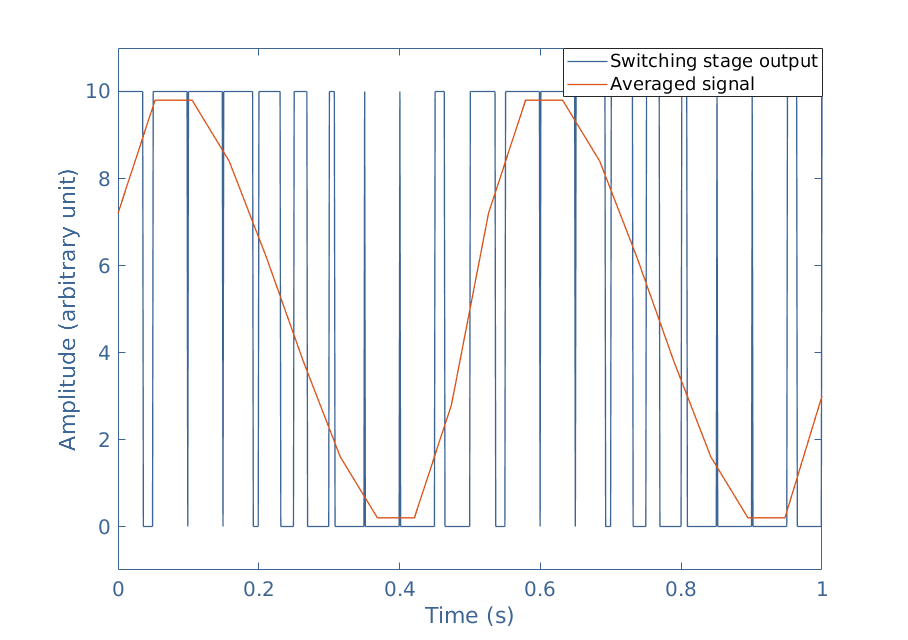
We can note that when the input signal is maximum, the PWM duty cycle tends to 1 and at the opposite, tends to 0 when the input signal is minimal. Therefore, the duty cycle of the PWM is directly related to the original shape of the sine signal. This affirmation can indeed be confirmed with a simple algorithm that averages the PWM output independently for each cycle, the result is plotted and shown in Figure 4 :
fig 4 : Average operation on the PWM signal
It is clear in this figure that when averaging the PWM signal, the sine shape of the original signal appears again. In real circuits, this operation is done by a filter as we will see in the section “Filtering”.
Amplification
Since the carrier signal is usually chosen such as its frequency is much higher than the input signal, the PWM output to amplify can be above the high cutoff frequency of a BJT-based amplifier (refer to the Frequency Response tutorial). This is the reason why high frequency MOS transistors are preferred over the classical bipolar-based amplifiers for class D amplification.
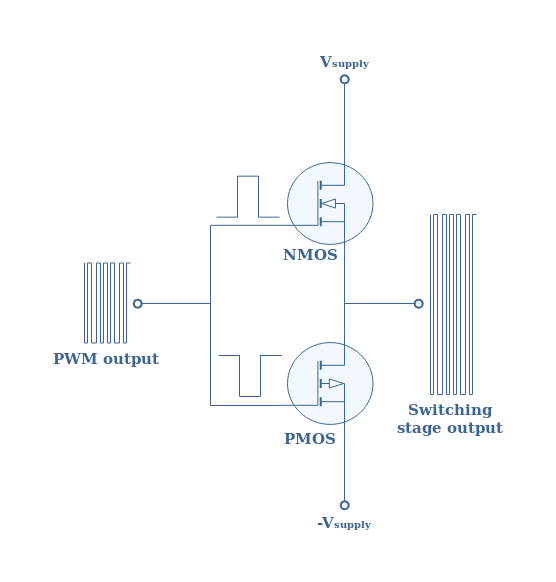
In a class D amplifiers, one NMOS and one PMOS are connected in a push-pull configuration as shown in Figure 5 :
fig 5 : Push-pull configuration of the amplification stage
Like for a class B amplifier, the complementary transistors are biased in such a way that the NMOS amplifies only positive half-waves and the PMOS only the negative half-waves. This amplification stage is also called the switching stage because the transistors behave precisely as switches : they are either fully ON (short circuit) or OFF (open circuit).
Filtering
In order to recover the original sine shape of the signal, the amplified pulse signal must be processed by a filter. This filter should respect some conditions :
Suppress the high frequencies above the normal bandwidth (midrange frequencies) of the amplifier, specially the carrier frequency and its harmonics.
Reproduce the midrange frequencies of the amplifier with a good level of gain. For example 20 Hz – 20 kHz for an audio amplifier.
Achieve a maximally flat band for the midrange frequencies.
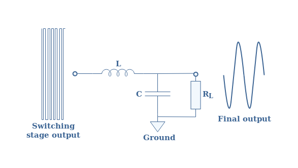
This kind of filter is commonly known as a Butterworth filter. The typical filter used to fulfill these requirements is a parallel LC circuit. When connected in parallel to a load RL, it actually can be seen as an RLC filter.
fig 6 : Low-pass L//C filter
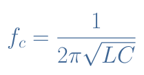
The bandwidth of this filter is characterized by its cutoff frequency fc at -3 dB that satisfies the Equation 1 :
eq 1 : Cutoff frequency of the low-pass filter
Moreover, since the RLC circuit is a second-order filter, a strong roll-off of -40 dB/dec is observed above fc. An asymptotic diagram of the frequency response of this filter is given is Figure 7 :
fig 7 : Second order Butterworth filter frequency response
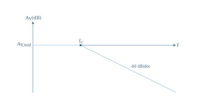
Several levels of parallel LC configurations are appreciated since each level increases the order of the filter and therefore the quality of filtration. In Figure 8, we can note the difference between the output resulting of a first or second order Butterworth filter applied to our example :
fig 8 : Difference of output between a first and second order Butterworth filter
Since the input signal has a frequency of 2 Hz and the carrier frequency is 20 Hz, a cutoff frequency of 4 Hz has been chosen for this filter. We can highlight the fact that a first order filter is not appropriate since it does not attenuate the carrier frequency enough while the second order filter output is much more sinusoidal.
Efficiency
The original way of functioning of the class D amplifier brings its efficiency to very high levels. This high efficiency is explained by the fact that the transistors behave nearly as ideal switches :
When they are OFF, no current IDS flows between the drain and the source.
When they are ON, no voltage VDS is observed across the drain and the source.
Therefore, no power VDS×IDS is dissipated in form of losses (heat). Typically the efficiency of class D amplifiers is above 90 %.
Conclusion
Class D amplifiers work very differently than the other typical classes (A,B,C). They are indeed, highly non-linear and incorporate special modules to treat the signals.
The first operation to be done is called a Pulse Width Modulation (PWM) and consists in comparing the input signal with a high frequency triangular signal. Whether the input is above the carrier or under, a new signal called the PWM output is generated and consists of a rectangular signal with the same frequency of the carrier but with a variable duty cycle. This signal is directly related to the original shape of the sine input.
Before getting back a sine signal, a switching stage made with two complementary NMOS and PMOS in a push-pull configuration amplifies the PWM output. The particularity of the transistors is that they switch between being fully ON or OFF, and they never work in their linear zone.
With this amplified pulse signal, a last stage that consists of a L//C circuit that acts as a Butterworth filter to recover the original sine shape. It is important to correctly set the cutoff frequency to eliminate the carrier frequency and its related harmonics. Moreover, a high order Butterworth filter is preferred to avoid as much as possible of distortion.
Finally, we have noted that the efficiency of this amplifier is noticeably higher than the typical classes because of the low power dissipation made possible by the switching behavior of the transistors. This fact is a great advantage in the design of class D amplifier : they do not require heavy and bulky heat sinks.
Due to its many advantages, class D amplifiers can be found in many daily applications : in mobile phones and many audio devices such as earphones, car radios etc …