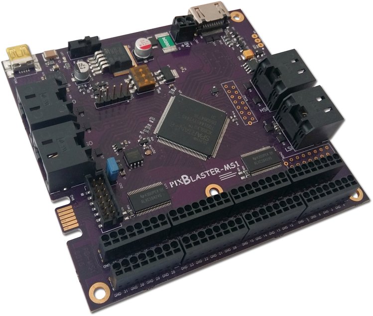
Combine LED strips to create a huge display that acts as a regular video monitor. All this with the FPGA based RGB LED controller that is capable of controlling up to 16,384 WS2812 based RGB LEDs at 60 FPS. Not only that, but you can daisy chain multiple controllers which can control up to hundreds of thousands of LEDs.
Due to their high cost and complexity, huge, shiny, beautiful video displays with thousands of LEDs have always been out of reach of enthusiasts and small business owners. Pixblasters MS1 changes all of that.
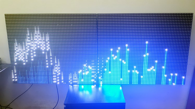
Pixblasters demo. Display made using LED strips glued to aluminum plates.
Pixblasters MS1 enables DIY enthusiasts and signage professionals, even those with minimal technical skills, to turn a bunch of addressable RGB LED strips into immense video LED displays. This FPGA-based LED controller enables new levels of professional-grade digital signage that cannot be attained by standard LED modules. The LED strips can be curved and glued to different surfaces to form giant yet economically viable video installations that can span entire buildings.
Key Features
Easy to use with any computer, any OS:
Pixblasters connects to any computer as an ordinary external monitor, with no programming needed. You can use it with Raspberry Pi, PC, media boxes, phones, etc. Simply plug in the monitor cable and the controller will smoothly drive the LEDs at the maximum frame-rate of 60 fps.
Straightforward display content and management:
Anything that shows in the selected part of monitor image shows on the LEDs as well. No need for special software for anti-aliasing or fonts. Use any digital signage software and add layered screen divisions, text, animations, video, RSS… LEDs work at their maximum speed and are perfectly synchronized, no matter the number of LEDs and chained MS1 controllers, or the display size.
Display size and resolution:
A single MS1 can control 4.7/17.7 m² (~ 50.6/190.5 ft²) while daisy-chained MS1s can control an LED display of hundreds of square meters using thirty to sixty LED strips. Daisy-chained controllers that drive a total of 16,384 LEDs can support HD LED displays.
Remote controllable and customizable:
Control it remotely from anywhere in the world through the network interfaces of the driving computer. Don’t worry about the LED display’s architecture. Users with special display applications (such as big, real-time timetables and scoreboards) can develop custom software for a computer monitor.
Open source FPGA demo:
Use the hardware platform for experimenting with, and learning about, driving RGB LEDs. Note: the open source FPGA demo design supports a subset of the fully-featured Pixblasters MS1 LED controller.
Features
Xilinx® Spartan®-6 XC6LX9-3 FPGA chip
On-board Microchip PIC18F26J50 microcontroller:
The microcontroller connects to the PC, runs the configuration software, and permanently stores the configuration data. It also enables simple firmware updates with any new features.
Output resolutions (H x V): 512 x 32 (native), 256 x 64, 128 x 128, 180 x 96, etc.
Board dimensions: 95 x 100 mm
LED details:
32 LED digital outputs: up to max. 512 LEDs per output
Maximum WS2812B/SK6812 LED display frame rate: 60 fps
Currently supported LED types: WS2811, WS2812, WS2812B, SK6812
Supports RGB666 (256K colors) color format
Maximum driving capacity of the single MS1 controller is 16,384 RGB LEDs
5 VDC 24 mA digital outputs compatible with the most popular RGB LED types
Connectivity:
HDMI video input allows for easy connection from the computer – it also works with adapter cables should your computer have a DVI® output
Push-in strip power and signal connectors enable easy wiring without soldering
Validated with different computers and different OS’s: Raspberry Pi Linux, Microsoft® Windows® PC, media boxes, phones and tablets…
On-board EDID flash enables automatic connection to any computer and any OS
Power:
Protected 5 VDC power supply input
The LED power supplies need to be wired separately to fulfill the power and current requirements of giant LED displays
Display controls:
Cropping image window
Display formatting
LED timing parameters
Supports different video resolutions (max. 720p – 1280 x 720 at 60 fps)
Integrated video input cropping and mirroring
Multiple lines per output mode
LED gamma correction
Daisy-chain multiple controllers:
Each MS1 board can work either as the Master or the Slave video controller
Daisy-chained controllers can drive more than 200,000 perfectly synchronized LEDs differently arranged in HD LED displays
The high-speed video link between MS1 boards assures max. fps and synchronicity
Low-speed control link interface
Video and control links use common UTP cables (Ethernet)
On-board DIP switches allow for an easy selection of the Master, Slave and six other FPGA configurations, including user-defined FPGA configurations
A single digital output has the ability drive multiple output video horizontal lines
Configuration is fully customizable through a menu on the PC connected via the USB serial cable
The project is live on Crowd Supply and basic pledge for Pixblasters Go costs $219.
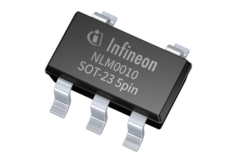
Infineon Technologies developed the NFC-PWM series (NLM0011 & NLM0010) for fast and cost effective implementation of NFC programming for LED drivers. The NFC programming can replace the labor intensive “plug-in resistor” current setting method with the contact less NFC interface. It improves the operational efficiency and flexibility in value chain by implementing automatic programming in the manufacturing line. With this it reduces the LED driver variants, simplifies the selection of LED modules, and allows end-of-line configuration.
The devices are NFC wireless configuration ICs with configurable PWM output primarily designed for LED applications. It enables cost effective NFC programming implementation by using a PWM signal directly to control the analog driver IC which eventually reduces the cost of BOM.
These devices can operate in two different modes, Active and Passive Mode. When the device is in passive mode the LED driver is not powered and the configurations of PWM parameters can be done via the NFC interface. When the device is in Active mode, it is powered by a Vcc Voltage supply, and a PWM output is generated according to the stored parameters. The PWM signal is converted into a desired DC voltage to control the current output of an LED driver by using an external R/C filter.
Constant light output (CLO) with 8 configurable points
Integrated operation-time counter (OTC) and on/off counter
Non-volatile memory (NVM) including UID and 20 bytes free memory for user data
Stable PWM output with fixed 2.8 V amplitude and +/-0.1% duty cycle accuracy
NLM0011 has the Integrated constant lumen output (CLO) function which compensated the luminous flux drop (aging effect) of the LED module by automatically adjusting the LED current to the aging characteristics of the LEDs. NLM0011 automatically adjusts the PWM duty cycle to compensate the LED degradation with the help of integrated operation time counter (OTC) and stored LED degradation curve in the CLO table.
There is no need for firmware development efforts as the device can fit perfectly to the mainstream analog driver ICs and can easily adapt into the existing designs to replace the “Plug-in- resistor” current configuration concept. The solution can easily go along with the existing analog LED driver designs and the NFC programming specification form the module –Driver interface special interest Group (MD-SIG). The NFC-PWM series can also be used in applications such as motor control and SMPS. The NLM0011 and NLM0010 can be ordered now in a SOT23-5 package, for more information you can use the datasheet or product page from Infineon.
Stepper motors are popular in computer and microcontroller-based position control applications like robotics, industrial automation, CNC machines, 3D printers and video camera control. Due to their uncomplicated internal construction and their limited number of connection wires, stepper motors look deceptively simple. On the internet, there are even lots of tutorials on how to control these motors using an antique L293D driver IC and an Arduino, but for serious applications everything depends on the quality and the capabilities of the motor driver.
After the release of several models of the One Mix mini laptops from One Netbook, like the One Mix 2S Yoga and the One Mix 3 Yoga, the company has recent just unveiled its intentions to launch another new model of the One Mix mini laptop called; One Mix 3 Pro, which is expected to come with an upgraded processing capacity for an improved performance for multi-threaded applications.
The upcoming One Mix 3 Pro is the first computer of its size to come with the 10th generation Intel Core “Comet Lake” processor. Instead of the 8th gen Core “Amber Lake” processors on previous models, the One Mix 3 Pro mini laptop is equipped with the Intel 10th generation Y-series Comet Lake processor – Comet Lake-Y Intel Core i5-10210Y processor with a 7W TDP – and designed for low power high performance output.
The mini laptop has dimensions 204 x 129 x 14.9mm, weighs around 660 grams and is allegedly said to be a convertible 2 in 1 tablet as it comes with a 360 degree hinge. It also comes with a 8.4 inch 2560 x 1600 pixel touch screen display, a backlit keyboard, and a fingerprint scanner for user input at the top right of the laptop. For system memory, the One Mix 3 pro comes with a dual channel 16GB LPDDR3 RAM, a microSD card reader and a 512GB NVMe SSD for storage.
Other features of the One Mix 3 Pro mini laptop include:
One micro HDMI port for video output
One USB “full function” type-C port and another USB 3.0 port for USB connection.
GPU – 24 EU Intel HD 615 graphics, up to 1.05GHz (300MHz – 1.05 GHz)
3.5mm audio jack and digital audio via HDMI
Mouse buttons, headset
Support for a 4096 degree of pressure-sensitive optional pen.
The One Mix mini laptop is expected to ship with a Windows 10 Home Edition operating system and should work with other version of windows. There is no word yet from One Netbook about pricing and availability of this mini laptop, but as one can guess, it should cost more than the previous One Mix models.
One Netbook plans to start selling the mini laptop in November, and they are likely to make it available through international resellers immediately after.
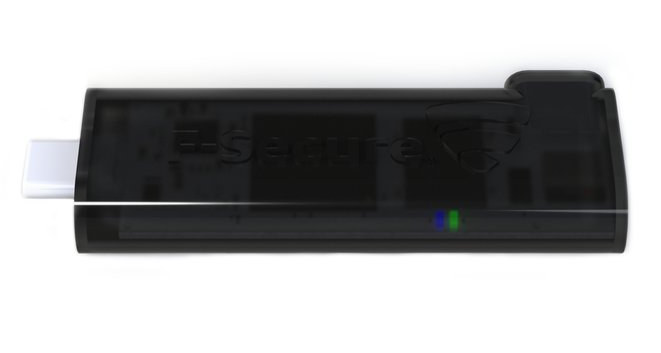
F-Secure Foundry recently launched a crowdfunding campaign for their new, tiny form factor USB Armory MK II computer. The device which comes with a form factor that looks like a usb flash drive is an open-source, full featured USB computer with Bluetooth, USB-C ports, 512MB RAM and 900MHz and was developed as an improvement to the USB Armory computer dongle launched far back in 2014.
The USB Armory MK II comes with the more efficient NXP i.MX6ULZ ARM Cortex TM – A7 processor, a 16GB eMMCflash memory chip and new security features like;
High Assurance Boot (HABv4) that enables the on-chip internal Boot ROM to authenticate the initial boot loader with a digital signature.
Secure non-volatile storage that includes a secure RTC, master key control, security state machine and tamper/violation detection and reporting.
True Random Number Generator which when included in the Linux kernels enables the component within the Linux framework.
External cryptographic co-processors (A71CH and ATECC) that provide high-endurance monotonic counters used for external verification of firmware rollback/downgrade attacks.
eMMC Replay Protected Memory Blocks that feature replay – protected authenticated access to flash memory using a shared connection between the eMMC and the host.
All of these features are not surprising, as, according to F-secure foundry, the USB MK11 was developed to help users with potential security applications like;
Password manager with integrated web server
OpenSSH client and agent for untrusted hosts
Router for end-to-end VPN tunneling
Portable penetration testing platform
Hardware security module
Tor bridge
Authentication token
Some of the highlight features of the USB Armoury MK11 hardware include;
NXP i.MX6ULZ ARM Cortex TM – A7 Processor at 900MHz
U-blox ANNA-B112 BLE Bluetooth module
512MB DDR3 RAM
USB 2.0 port and 2 USB type-C ports (Dual Role Power Receptacle and Upstream Facing Port
Small form factor (Dimension – 66mm x 19mm x 8mm )
Slide switch for boot mode selection between microSD and eMMC
External security elements – NXPA71CH + Microchip ATECC608A
Intro Video
The NXP i.MX6ULZ ARM Cortex TM – A7 processor along with superior speed (900MHz) and other features that meet current trend like USB-C ports are some of elements that gives the new MK11 an edge over the earlier MK1. A summary of the features of both boards is provided in the table below to highlight the difference between them.
The USB Armory MK II supports full TCP/IP connection to/from it via USB CDC Ethernet emulation along with wireless connectivity over BLE, and serial communication over USB or physical UART using the Debug board. It should be noted that HDMI video is not supported over the 2 USB-C ports; only the USB 2.0 protocol is supported over the USB-C ports.
More details on the USB Armory MK II and the Crowdfunding campaign can be found on the project page on Crowdsupply. Over $20000 has already been committed by backers and all orders are expected to be shipped by the end of 2019 or in early 2020 with free shipping to backers in the US and a $15 service charge to ship to the rest of the world.
Taiwanese startup Mikro Mesa Technology has announced a major breakthrough in the mass transfer of microLEDs, with a non-compression low temperature bonding process allowing millions of microLEDs to be transferred in one step. by Julien Happich @ www.eenewsled.com
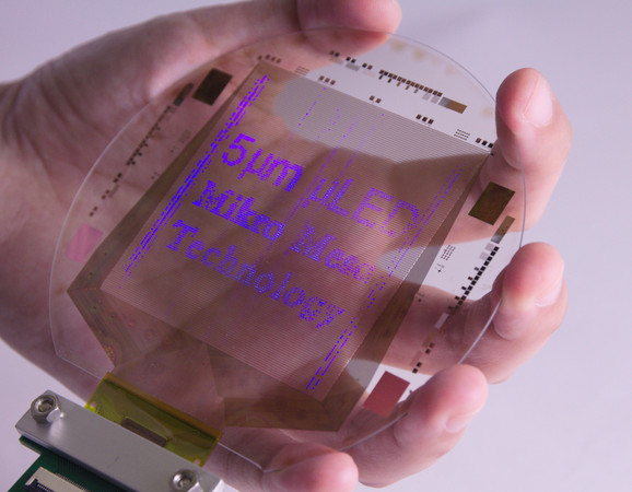
Blue-green two-color pixel structure at a pitch of under 5µm. (Photo/Mikro Mesa)
The company started cooperation with Chinese custom LCD display manufacturer Nanjing CLP Panda in 2017 and it took two years of development to deliver the first 3µm microLED chips. The ultra-small pixels means more microLEDs come out of the epitaxial wafers, and the mass transfer from wafers as large as 4-inch in diametre means up to millions of pixels can be transferred at a time, including multi-color microLEDs arrays. The large transfer area also reduces the number of necessary transfers for the production of large-size full-color displays, increasing yield.
According to Mikro Mesa insiders, the display technology can produce high-precision displays up to 1,800 dpi and could be applied to 55-inch or higher microLED TVs. The company anticipates the mass transfer process will make its microLEDs competitive with OLEDs for screens in wearables, smart phones, and AR headsets.
5µm die display samples made with Mikro Mesa’s massive transfer technology. (Photo/Mikro Mesa).
What’s more, due to its low process temperature, the technology is compatible with flexible and transparent substrates, enabling the design of transparent displays with much higher performance than today’s AMOLED displays.
Reflow ovens are an important part of the development of PCB for electronic products when using surface mount components. They provide a route through which PCBs can be quickly populated with SMD components, however, for accurate results, the heat across the oven needs to be controlled and timed correctly. To achieve this, manufacturers use a kind of controller, like “TinyReflow Controller”, and with several DIY reflow ovens being used by makers around the world, we thought it would be a good fit for today’s tutorial to focus on the development of DIY Reflow Oven Controller.
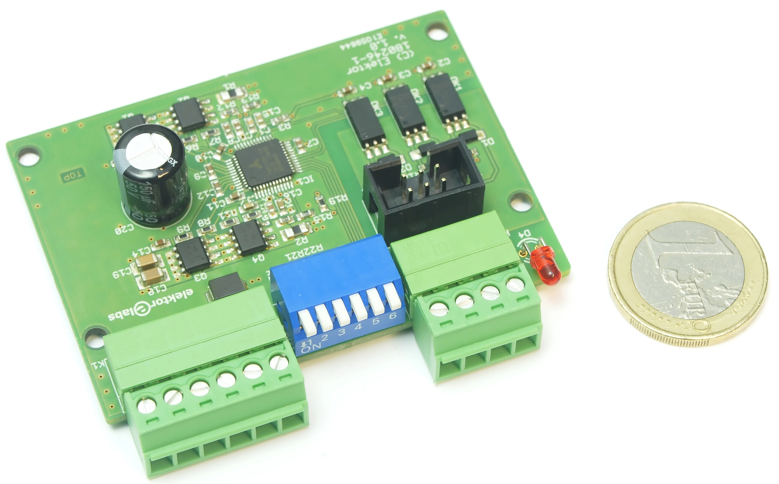
As mentioned above, reflow oven controllers are quite important in ensuring just the right amount of heat is applied in the soldering process for SMD components and this importance has led to the development of quite a number of different Reflow oven controller projects, which someone can find on the internet. However, for today’s tutorial, we will look at the first version of Rocket Stream’s tiny Reflow Oven Controller v1 which is probably the most well tested DIY reflow oven controller on the internet, as it is the one being used by Rocket Stream themselves for the manufacturing of their boards.
Tiny Reflow Controller with character LCD – [Link]
Reflow ovens are an important part of the development of PCB for electronic products when using surface mount components. They provide a route through which PCBs can be quickly populated with SMD components, however, for accurate results, the heat across the oven needs to be controlled and timed correctly. To achieve this, manufacturers use a kind of controller, like “TinyReflow Controller”, and with several DIY reflow ovens being used by makers around the world, we thought it would be a good fit for today’s tutorial to focus on the development of DIY Reflow Oven Controller.
As mentioned above, reflow oven controllers are quite important in ensuring just the right amount of heat is applied in the soldering process for SMD components and this importance has led to the development of quite a number of different Reflow oven controller projects, which someone can find on the internet. However, for today’s tutorial, we will look at the first version of Rocket Stream’s tiny Reflow Oven Controller v1 which is probably the most well tested DIY reflow oven controller on the internet, as it is the one being used by Rocket Stream themselves for the manufacturing of their boards.
The Rocket Stream’s Reflow Oven Controller v1 is powered by the ATtiny1634R and uses the latest thermocouple sensor interface IC MAX31856 from Maxim. It is one of the cheapest designs on the internet as Rocket Stream was able to reduce the overall cost of the design by not using a development board like the Arduino and using as many SMD parts as possible in place of through-hole components, to reduce the time that goes in and the work involved leaving only the terminal block and the LCD connector as the only through-hole components.
The ATtiny1634R is one of the new ATtinys we discussed in the last article. It is a High Performance, Low Power AVR® 8-bit Microcontroller with Advanced RISC Architecture, 16K Bytes of In-System, Self-Programmable Flash Program Memory and 256 Bytes of In-System Programmable EEPROM with support for up to 100,000 Write/Erase Cycles. It comes In-System Programmable via SPI Port and can be programmed using the Arduino IDE.
Other components involved include an external Solid State Relay (SSR) which should be rated according to the current draw of your oven (heater) and a K type thermocouple which provides temperature feedback to the controller and an LCD on which information/status of the system is displayed.
At the end of this project, you know the workings behind the Tiny Reflow Controller and you will have built up the courage required to attempt building one by yourself.
Required Components
The following main components are required to build the project:
ATtiny1634R
MAX31856 thermocouple interface
K-Type Thermocouple(Rocket stream recommends those with fiberglass or steel jacket
8×2 LCD black character with yellow backlight
2 push button
1 red LED
2 Terminal Blocks
1 Transistor
1 Buzzer
Yes you guessed right. The list is definitely longer than this but so things doesn’t get messy, other components that are required are provided in the table below
Component Count: 51
Ref
Qnty
Value
C1, C2
2
10nF
C3, C6, C7, C8, C9
5
100nF
C4, C5
2
1uF 16V X7R
C10, C11, C12
3
10uF 10V X5R
D1
1
Red
D2
1
PMEG3020CPA
D3
1
1N4148WS
J1, J2
2
TERMINAL-BLOCK-1×2
J3
1
MICRO-USB
J4
1
2.54mm 2×3
J5
1
2.54mm 1×6
L1
1
BLM18KG221SN1D
LOGO1
1
LOGO-ROCKET-SCREAM
LOGO2
1
LOGO-KICAD
LOGO3
1
LOGO-ROCKET-SCREAM
LOGO4
1
LOGO-OSHW
LS1
1
HYG9605B
M5, M6
2
FIDUCIAL
Q1, Q2
2
2N3904
R1
1
35WR10KLFTR
R2, R3
2
100R
R4, R5, R9, R10
4
10K
R6
1
2K2
R7
1
27K
R8
1
53K6
SW1, SW2
2
IT-1109S
SW3
1
TS-018
U1
1
ATTINY1634R-MU
U2
1
MCP1700T-3302E/MB
U3
1
MAX31856
U4
1
RT0802A
This BOM is also attached in the zip file under the download section and could be used to place the order for all the components at once.
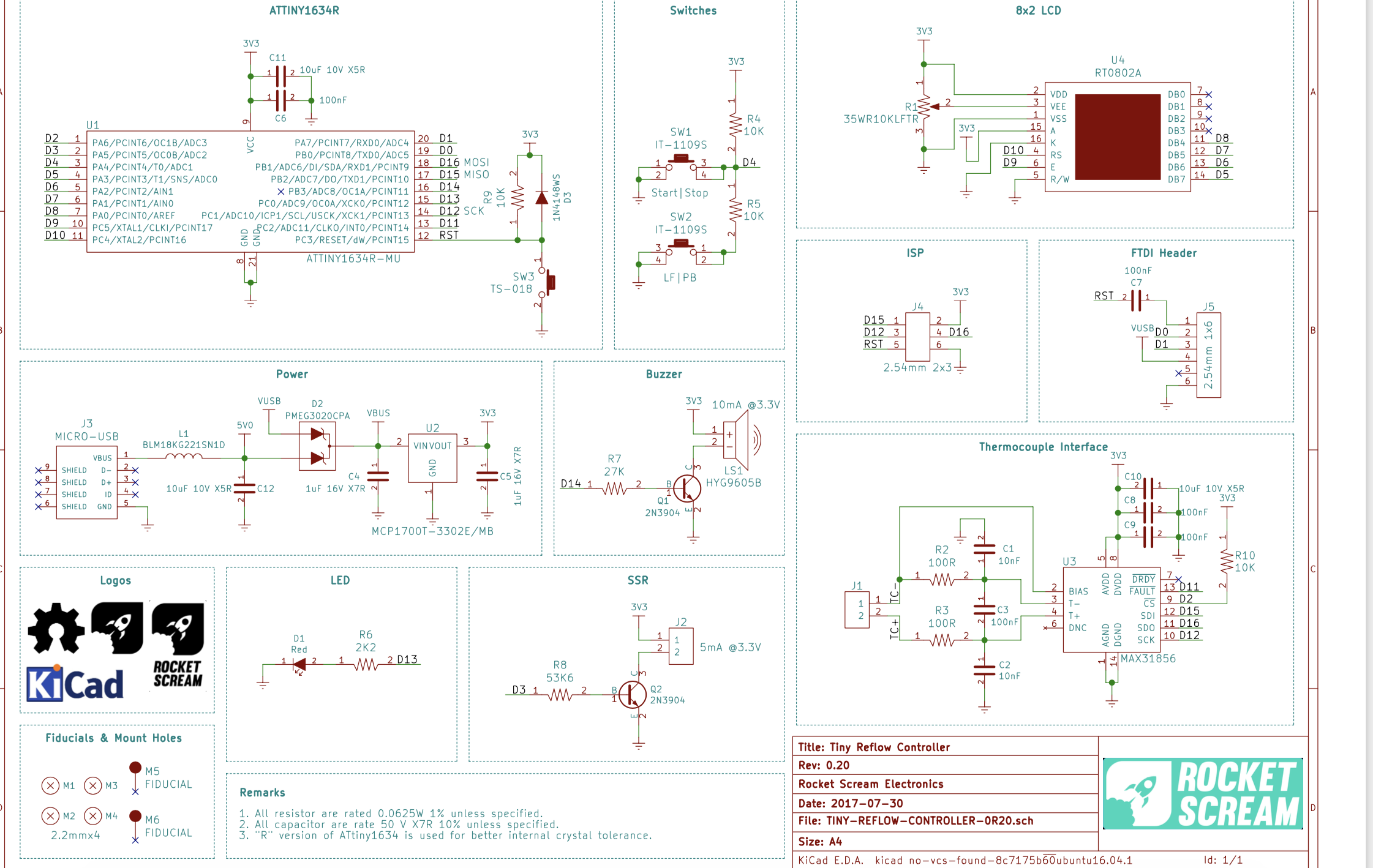
Schematics
Since most of the components to be used are SMD, it only makes sense to implement this project on a PCB. However, users can choose to get the through-hole version of the components so it can be implemented on a breadboard. The schematics for the project is shown in the image below.
Tiny Reflow Controller v1 schematic
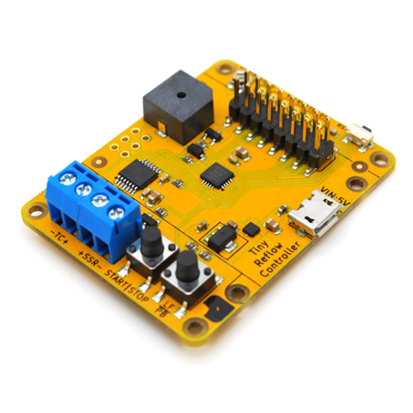
The schematics and the resulting PCB were developed with KICAD and the files are attached in the zip file under the download section. You can edit the design to make whatever modification you want or just use the Gerber files which have already been generated to produce your own PCB. An image of the tiny reflow oven controller is shown below.
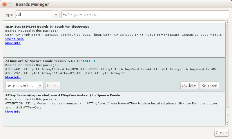
We will use the Arduino IDE to develop the code for today’s project, as such, you will need to install the Arduino IDE board support files for the ATTINY1634R microcontroller so it can be programmed using the Arduino IDE. Check out our tutorial on setting up the Arduino IDE to program ATtiny based microcontrollers to get some help.
The sketch for today’s project is based on the example code shipped by Rocket Stream. It runs the reflow process via a PID control algorithm that is based on the awesome Arduino PID library written by Brett Beauregard. The sketch simply evaluates the current heat level, compares it with what the value should be at that particular reflow stage and adjust itself using the PID algorithms to ensure it’s up to par.
Asides the PID Library, other libraries used for the project include; the Liquid Crystal Library which was used to interface with the LCD, the Adafruit Max31856 library which was used to interface with the thermocouple, and the Arduino EEPROM library which was used to manage the storage and extraction of data on the EEPROM. While the EEPROM library comes with the Arduino IDE, the other libraries can be installed via the Arduino library manager.
As usual, I will do a brief explanation of the code highlighting the major parts. The example code we will work with, takes into account both leaded and lead-free reflow oven configurations, allowing users to change from one to the other via a push button.
We start the sketch by including all the libraries that we will use, after which we create a type definition that holds several parameters to indicate the state of the reflow process.
Next, we create variables to hold constant values that will be used irrespective of the profile selected (General Profile constant) and we follow it up by creating variables to hold values specific to Lead-free profile and also create those specific to the leaded profile. This ensures that irrespective of the profile selected by the user, the necessary information will be available.
Next, we create variables to be used by the PID Algorithm, followed by LCD messages and a few other variables. The names are very descriptive so it should be easy to follow.
// ***** PID PARAMETERS *****
// ***** PRE-HEAT STAGE *****
#define PID_KP_PREHEAT 100
#define PID_KI_PREHEAT 0.025
#define PID_KD_PREHEAT 20
// ***** SOAKING STAGE *****
#define PID_KP_SOAK 300
#define PID_KI_SOAK 0.05
#define PID_KD_SOAK 250
// ***** REFLOW STAGE *****
#define PID_KP_REFLOW 300
#define PID_KI_REFLOW 0.05
#define PID_KD_REFLOW 350
#define PID_SAMPLE_TIME 1000

// ***** LCD MESSAGES *****
const char* lcdMessagesReflowStatus[] = {
  "Ready",
  "Pre",
  "Soak",
  "Reflow",
  "Cool",
  "Done!",
  "Hot!",
  "Error"
};

// ***** DEGREE SYMBOL FOR LCD *****
unsigned char degree[8]  = {
  140, 146, 146, 140, 128, 128, 128, 128
};

// ***** PIN ASSIGNMENT *****
int ssrPin = 3;
int thermocoupleCSPin = 2;
int lcdRsPin = 10;
int lcdEPin = 9;
int lcdD4Pin = 8;
int lcdD5Pin = 7;
int lcdD6Pin = 6;
int lcdD7Pin = 5;
int buzzerPin = 14;
int switchPin = A1;

// ***** PID CONTROL VARIABLES *****
double setpoint;
double input;
double output;
double kp = PID_KP_PREHEAT;
double ki = PID_KI_PREHEAT;
double kd = PID_KD_PREHEAT;
int windowSize;
unsigned long windowStartTime;
unsigned long nextCheck;
unsigned long nextRead;
unsigned long updateLcd;
unsigned long timerSoak;
unsigned long buzzerPeriod;
unsigned char soakTemperatureMax;
unsigned char reflowTemperatureMax;
unsigned long soakMicroPeriod;
// Reflow oven controller state machine state variable
reflowState_t reflowState;
// Reflow oven controller status
reflowStatus_t reflowStatus;
// Reflow profile type
reflowProfile_t reflowProfile;
// Switch debounce state machine state variable
debounceState_t debounceState;
// Switch debounce timer
long lastDebounceTime;
// Switch press status
switch_t switchStatus;
switch_t switchValue;
switch_t switchMask;
// Seconds timer
int timerSeconds;
// Thermocouple fault status
unsigned char fault;
With all the variables created, we then create an instance of the PID, the LiquidCrystal, and the MAX31856 libraries after which we move to the void setup() function.
We start the void setup() function by checking the currently selected reflow profile on the EEPROM this helps determine which of the variable groups should be selected. If no reflow profile was previously stored, the system selects the Leadfree profile as default.
void setup()
{
  // Check current selected reflow profile
  unsigned char value = EEPROM.read(PROFILE_TYPE_ADDRESS);
  if ((value == 0) || (value == 1))
  {
    // Valid reflow profile value
    reflowProfile = value;
  }
  else
  {
    // Default to lead-free profile
    EEPROM.write(PROFILE_TYPE_ADDRESS, 0);
    reflowProfile = REFLOW_PROFILE_LEADFREE;
  }
Next, we initialize the SSR pin to ensure the reflow oven is open after which we initialize the buzzer setting it to turn on immediately the system powers up.
// SSR pin initialization to ensure reflow oven is off
  digitalWrite(ssrPin, LOW);
  pinMode(ssrPin, OUTPUT);

  // Buzzer pin initialization to ensure annoying buzzer is off
  digitalWrite(buzzerPin, LOW);
  pinMode(buzzerPin, OUTPUT);

  // LED pins initialization and turn on upon start-up (active high)
  pinMode(LED_BUILTIN, OUTPUT);
  digitalWrite(LED_BUILTIN, HIGH);
We also initialize the thermocouple, indicating the type, and also initialize the LCD and display a sort of splash screen with the date and version of the controller.
Next, we initialize serial communication, turn off the Status LED, and initialize the variables we will use to monitor time as the sketch runs.
// Serial communication at 115200 bps
  Serial.begin(115200);

  // Turn off LED (active high)
  digitalWrite(LED_BUILTIN, LOW);
  // Set window size
  windowSize = 2000;
  // Initialize time keeping variable
  nextCheck = millis();
  // Initialize thermocouple reading variable
  nextRead = millis();
  // Initialize LCD update timer
  updateLcd = millis();
}
With this done, we move to the void loop() function where all the major actions take place.
The code for the void loop() function is quite bulky but the idea is simple. We use the variables earlier created for time tracking to manage the reflow process, monitoring the amount of heat with the thermostat, and using that information as an input into the PID algorithm which then determines how the heater operates. For each stage in the reflow process, the PID operates in such a way that the designated amount of heat for that stage is achieved. While all of this is going on, the time and temperature information are also being displayed on the screen to provide visual feedback to the user and the switches which are used to set the reflow status and the reflow profile are also being watched so the system can act immediately on any change in their state.
void loop()
{
  // Current time
  unsigned long now;

  // Time to read thermocouple?
  if (millis() > nextRead)
  {
    // Read thermocouple next sampling period
    nextRead += SENSOR_SAMPLING_TIME;
    // Read current temperature
    input = thermocouple.readThermocoupleTemperature();
    // Check for thermocouple fault
    fault = thermocouple.readFault();

    // If any thermocouple fault is detected
    if ((fault & MAX31856_FAULT_CJRANGE) ||
        (fault & MAX31856_FAULT_TCRANGE) ||
        (fault & MAX31856_FAULT_CJHIGH) ||
        (fault & MAX31856_FAULT_CJLOW) ||
        (fault & MAX31856_FAULT_TCHIGH) ||
        (fault & MAX31856_FAULT_TCLOW) ||
        (fault & MAX31856_FAULT_OVUV) ||
        (fault & MAX31856_FAULT_OPEN))
    {
      // Illegal operation
      reflowState = REFLOW_STATE_ERROR;
      reflowStatus = REFLOW_STATUS_OFF;
    }
  }

  if (millis() > nextCheck)
  {
    // Check input in the next seconds
    nextCheck += 1000;
    // If reflow process is on going
    if (reflowStatus == REFLOW_STATUS_ON)
    {
      // Toggle red LED as system heart beat
      digitalWrite(LED_BUILTIN, !(digitalRead(LED_BUILTIN)));
      // Increase seconds timer for reflow curve analysis
      timerSeconds++;
      // Send temperature and time stamp to serial
      Serial.print(timerSeconds);
      Serial.print(",");
      Serial.print(setpoint);
      Serial.print(",");
      Serial.print(input);
      Serial.print(",");
      Serial.println(output);
    }
    else
    {
      // Turn off red LED
      digitalWrite(LED_BUILTIN, LOW);
    }
  }

  if (millis() > updateLcd)
  {
    // Update LCD in the next 250 ms
    updateLcd += 250;
    // Clear LCD
    lcd.clear();
    // Print current system state
    lcd.print(lcdMessagesReflowStatus[reflowState]);
    lcd.setCursor(6, 0);
    if (reflowProfile == REFLOW_PROFILE_LEADFREE)
    {
      lcd.print("LF");
    }
    else
    {
      lcd.print("PB");
    }
    // Move the cursor to the 2 line
    lcd.setCursor(0, 1);

    // If currently in error state
    if (reflowState == REFLOW_STATE_ERROR)
    {
      // Thermocouple error (open, shorted)
      lcd.print("TC Error");
    }
    else
    {
      // Display current temperature
      lcd.print(input);

#if ARDUINO >= 100
      // Display degree Celsius symbol
      lcd.write((uint8_t)0);
#else
      // Display degree Celsius symbol
      lcd.print(0, BYTE);
#endif
      lcd.print("C ");
    }
  }

  // Reflow oven controller state machine
  switch (reflowState)
  {
    case REFLOW_STATE_IDLE:
      // If oven temperature is still above room temperature
      if (input >= TEMPERATURE_ROOM)
      {
        reflowState = REFLOW_STATE_TOO_HOT;
      }
      else
      {
        // If switch is pressed to start reflow process
        if (switchStatus == SWITCH_1)
        {
          // Send header for CSV file
          Serial.println("Time,Setpoint,Input,Output");
          // Intialize seconds timer for serial debug information
          timerSeconds = 0;
          // Initialize PID control window starting time
          windowStartTime = millis();
          // Ramp up to minimum soaking temperature
          setpoint = TEMPERATURE_SOAK_MIN;
          // Load profile specific constant
          if (reflowProfile == REFLOW_PROFILE_LEADFREE)
          {
            soakTemperatureMax = TEMPERATURE_SOAK_MAX_LF;
            reflowTemperatureMax = TEMPERATURE_REFLOW_MAX_LF;
            soakMicroPeriod = SOAK_MICRO_PERIOD_LF;
          }
          else
          {
            soakTemperatureMax = TEMPERATURE_SOAK_MAX_PB;
            reflowTemperatureMax = TEMPERATURE_REFLOW_MAX_PB;
            soakMicroPeriod = SOAK_MICRO_PERIOD_PB;
          }
          // Tell the PID to range between 0 and the full window size
          reflowOvenPID.SetOutputLimits(0, windowSize);
          reflowOvenPID.SetSampleTime(PID_SAMPLE_TIME);
          // Turn the PID on
          reflowOvenPID.SetMode(AUTOMATIC);
          // Proceed to preheat stage
          reflowState = REFLOW_STATE_PREHEAT;
        }
      }
      break;

    case REFLOW_STATE_PREHEAT:
      reflowStatus = REFLOW_STATUS_ON;
      // If minimum soak temperature is achieve
      if (input >= TEMPERATURE_SOAK_MIN)
      {
        // Chop soaking period into smaller sub-period
        timerSoak = millis() + soakMicroPeriod;
        // Set less agressive PID parameters for soaking ramp
        reflowOvenPID.SetTunings(PID_KP_SOAK, PID_KI_SOAK, PID_KD_SOAK);
        // Ramp up to first section of soaking temperature
        setpoint = TEMPERATURE_SOAK_MIN + SOAK_TEMPERATURE_STEP;
        // Proceed to soaking state
        reflowState = REFLOW_STATE_SOAK;
      }
      break;

    case REFLOW_STATE_SOAK:
      // If micro soak temperature is achieved
      if (millis() > timerSoak)
      {
        timerSoak = millis() + soakMicroPeriod;
        // Increment micro setpoint
        setpoint += SOAK_TEMPERATURE_STEP;
        if (setpoint > soakTemperatureMax)
        {
          // Set agressive PID parameters for reflow ramp
          reflowOvenPID.SetTunings(PID_KP_REFLOW, PID_KI_REFLOW, PID_KD_REFLOW);
          // Ramp up to first section of soaking temperature
          setpoint = reflowTemperatureMax;
          // Proceed to reflowing state
          reflowState = REFLOW_STATE_REFLOW;
        }
      }
      break;

    case REFLOW_STATE_REFLOW:
      // We need to avoid hovering at peak temperature for too long
      // Crude method that works like a charm and safe for the components
      if (input >= (reflowTemperatureMax - 5))
      {
        // Set PID parameters for cooling ramp
        reflowOvenPID.SetTunings(PID_KP_REFLOW, PID_KI_REFLOW, PID_KD_REFLOW);
        // Ramp down to minimum cooling temperature
        setpoint = TEMPERATURE_COOL_MIN;
        // Proceed to cooling state
        reflowState = REFLOW_STATE_COOL;
      }
      break;

    case REFLOW_STATE_COOL:
      // If minimum cool temperature is achieve
      if (input <= TEMPERATURE_COOL_MIN)
      {
        // Retrieve current time for buzzer usage
        buzzerPeriod = millis() + 1000;
        // Turn on buzzer to indicate completion
        digitalWrite(buzzerPin, HIGH);
        // Turn off reflow process
        reflowStatus = REFLOW_STATUS_OFF;
        // Proceed to reflow Completion state
        reflowState = REFLOW_STATE_COMPLETE;
      }
      break;

    case REFLOW_STATE_COMPLETE:
      if (millis() > buzzerPeriod)
      {
        // Turn off buzzer
        digitalWrite(buzzerPin, LOW);
        // Reflow process ended
        reflowState = REFLOW_STATE_IDLE;
      }
      break;

    case REFLOW_STATE_TOO_HOT:
      // If oven temperature drops below room temperature
      if (input < TEMPERATURE_ROOM)
      {
        // Ready to reflow
        reflowState = REFLOW_STATE_IDLE;
      }
      break;

    case REFLOW_STATE_ERROR:
      // Check for thermocouple fault
      fault = thermocouple.readFault();

      // If thermocouple problem is still present
      if ((fault & MAX31856_FAULT_CJRANGE) ||
          (fault & MAX31856_FAULT_TCRANGE) ||
          (fault & MAX31856_FAULT_CJHIGH) ||
          (fault & MAX31856_FAULT_CJLOW) ||
          (fault & MAX31856_FAULT_TCHIGH) ||
          (fault & MAX31856_FAULT_TCLOW) ||
          (fault & MAX31856_FAULT_OVUV) ||
          (fault & MAX31856_FAULT_OPEN))
      {
        // Wait until thermocouple wire is connected
        reflowState = REFLOW_STATE_ERROR;
      }
      else
      {
        // Clear to perform reflow process
        reflowState = REFLOW_STATE_IDLE;
      }
      break;
  }

  // If switch 1 is pressed
  if (switchStatus == SWITCH_1)
  {
    // If currently reflow process is on going
    if (reflowStatus == REFLOW_STATUS_ON)
    {
      // Button press is for cancelling
      // Turn off reflow process
      reflowStatus = REFLOW_STATUS_OFF;
      // Reinitialize state machine
      reflowState = REFLOW_STATE_IDLE;
    }
  }
  // Switch 2 is pressed
  else if (switchStatus == SWITCH_2)
  {
    // Only can switch reflow profile during idle
    if (reflowState == REFLOW_STATE_IDLE)
    {
      // Currently using lead-free reflow profile
      if (reflowProfile == REFLOW_PROFILE_LEADFREE)
      {
        // Switch to leaded reflow profile
        reflowProfile = REFLOW_PROFILE_LEADED;
        EEPROM.write(PROFILE_TYPE_ADDRESS, 1);
      }
      // Currently using leaded reflow profile
      else
      {
        // Switch to lead-free profile
        reflowProfile = REFLOW_PROFILE_LEADFREE;
        EEPROM.write(PROFILE_TYPE_ADDRESS, 0);
      }
    }
  }
  // Switch status has been read
  switchStatus = SWITCH_NONE;

  // Simple switch debounce state machine (analog switch)
  switch (debounceState)
  {
    case DEBOUNCE_STATE_IDLE:
      // No valid switch press
      switchStatus = SWITCH_NONE;

      switchValue = readSwitch();

      // If either switch is pressed
      if (switchValue != SWITCH_NONE)
      {
        // Keep track of the pressed switch
        switchMask = switchValue;
        // Intialize debounce counter
        lastDebounceTime = millis();
        // Proceed to check validity of button press
        debounceState = DEBOUNCE_STATE_CHECK;
      }
      break;

    case DEBOUNCE_STATE_CHECK:
      switchValue = readSwitch();
      if (switchValue == switchMask)
      {
        // If minimum debounce period is completed
        if ((millis() - lastDebounceTime) > DEBOUNCE_PERIOD_MIN)
        {
          // Valid switch press
          switchStatus = switchMask;
          // Proceed to wait for button release
          debounceState = DEBOUNCE_STATE_RELEASE;
        }
      }
      // False trigger
      else
      {
        // Reinitialize button debounce state machine
        debounceState = DEBOUNCE_STATE_IDLE;
      }
      break;

    case DEBOUNCE_STATE_RELEASE:
      switchValue = readSwitch();
      if (switchValue == SWITCH_NONE)
      {
        // Reinitialize button debounce state machine
        debounceState = DEBOUNCE_STATE_IDLE;
      }
      break;
  }

  // PID computation and SSR control
  if (reflowStatus == REFLOW_STATUS_ON)
  {
    now = millis();

    reflowOvenPID.Compute();

    if ((now - windowStartTime) > windowSize)
    {
      // Time to shift the Relay Window
      windowStartTime += windowSize;
    }
    if (output > (now - windowStartTime)) digitalWrite(ssrPin, HIGH);
    else digitalWrite(ssrPin, LOW);
  }
  // Reflow oven process is off, ensure oven is off
  else
  {
    digitalWrite(ssrPin, LOW);
  }
}
The complete code is attached along with the other files under the download section.
Programming the ATtiny1634R
The board provides a standard FTDI (or compatible) USB-serial 6-pin breakout which can be used to upload firmware to the onboard mcu. This can done through the Arduino IDE. The on-board ATtiny1634R microcontroller uses the ATtinyCore written by Spence Konde. All you have to do is to install the ATtinyCore through the Arduino IDE Boards Manager. Prior to this you will have to burn ATtinyCore bootloader to the mcu. You can use an AVRISP mkII (or any of the AVR programmer supported on the IDE) to program the bootloader onto the ATtiny1634R. To program the bootloader, you connect the standard 6-pin AVR ISP (2×3 pins 2.54 mm) to the AVRISP mkII programmer. Then you hit “burn bootloader” after selecting the correct board option. Once the bootloader is in, then you can use the FTDI USB-serial to upload code normally from Arduino IDE.
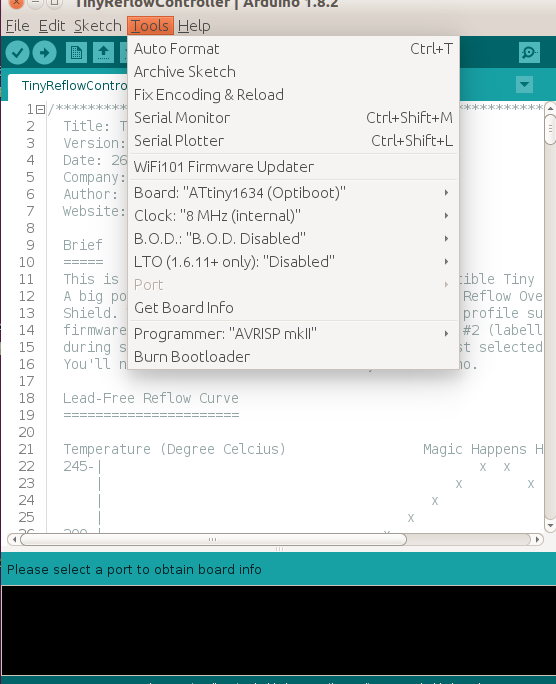
Once the ATtinyCore board package has been installed, you should select ATtiny1634 (Optiboot) with the 8 MHz internal clock:
Demo
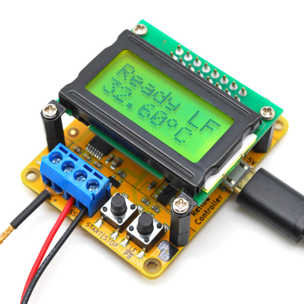
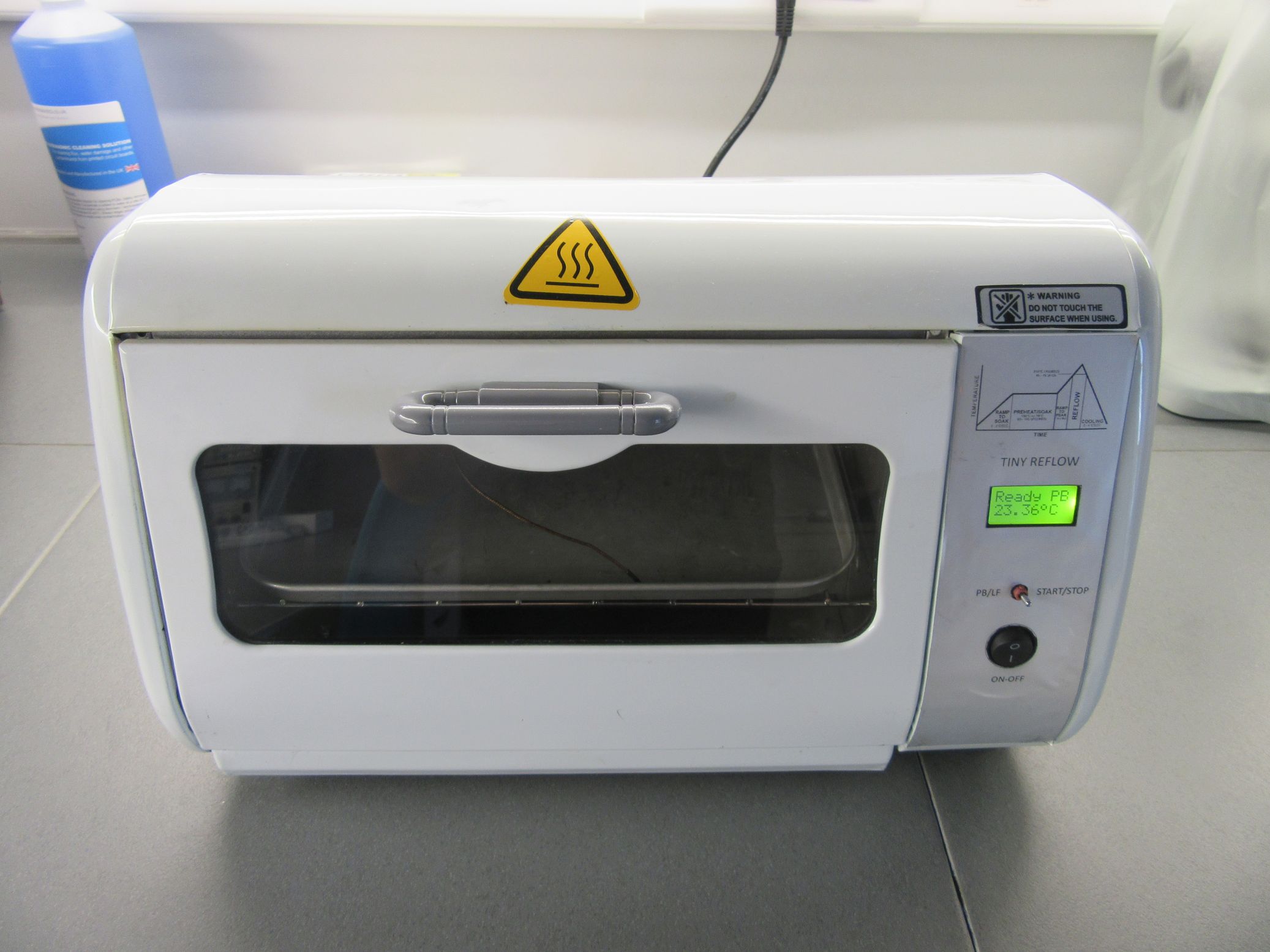
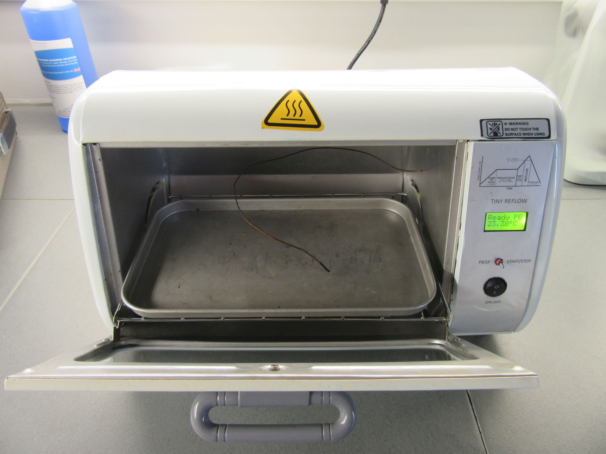
The PCB version of the reflow controller comes with an FTDI interface through which it can be programmed so if you are building on a breaboard, ensure you make provision for that too. Using a FTDI to USB Cable, connect the setup to your computer. Select the board type and upload the code to it. With this done, you can now connect your tiny reflow oven controller to your oven and power it on. You should see the splash come up with a screen similar to the image below.
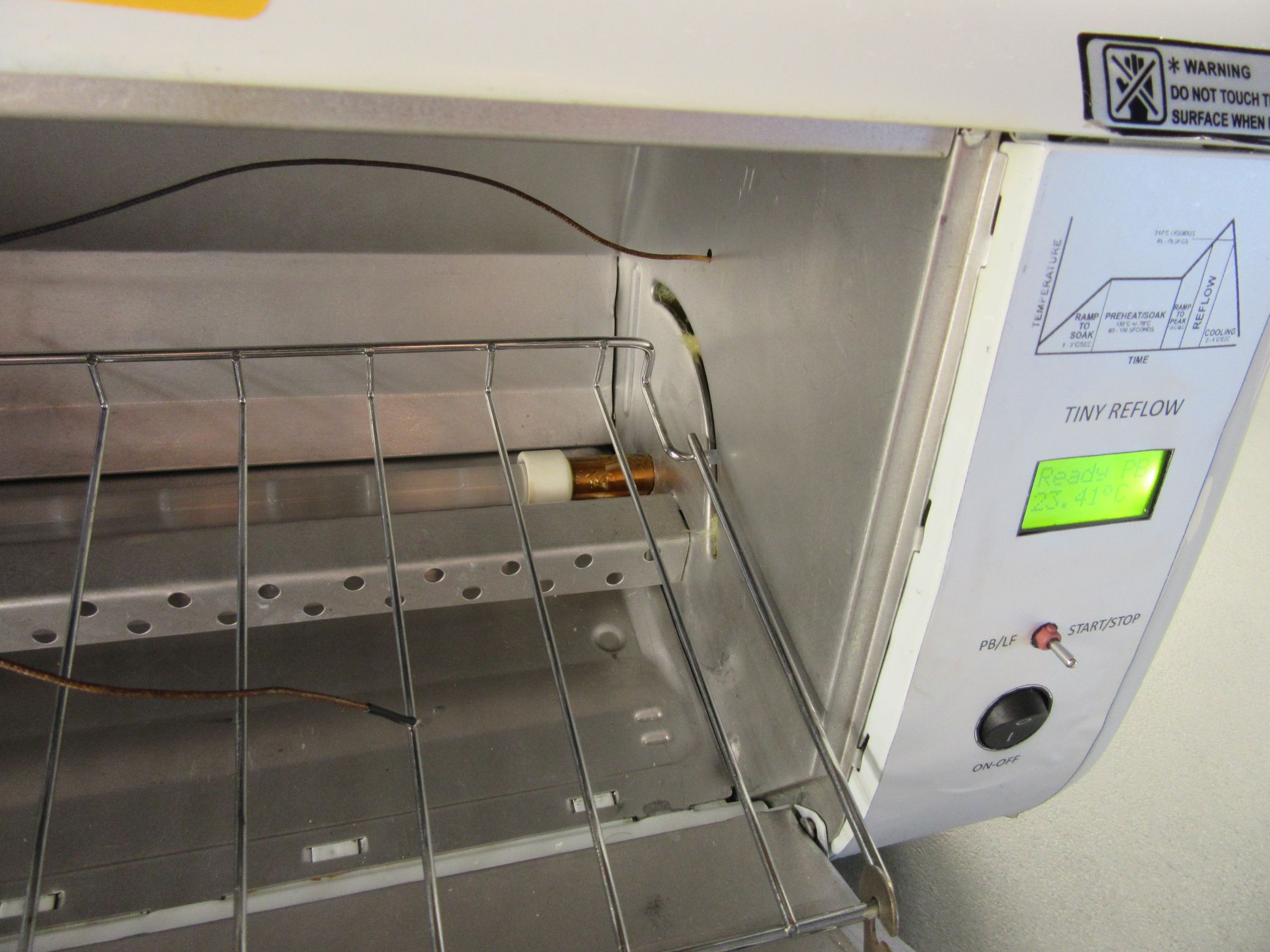
Installation on the mini Oven
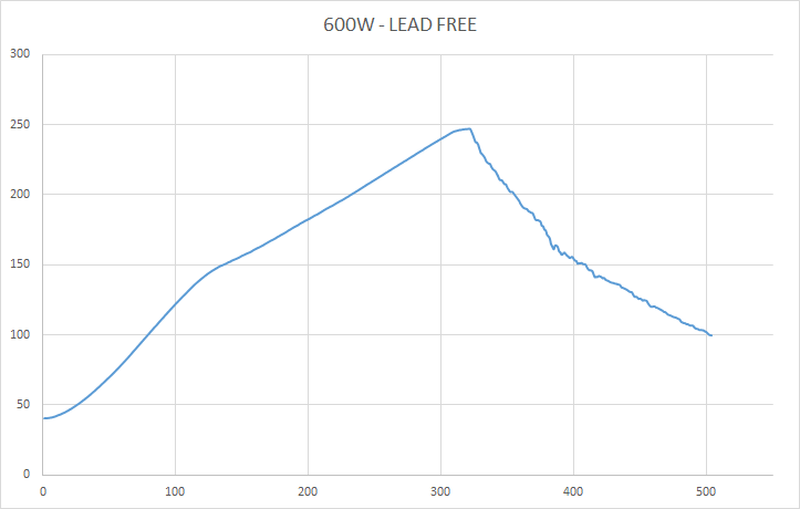
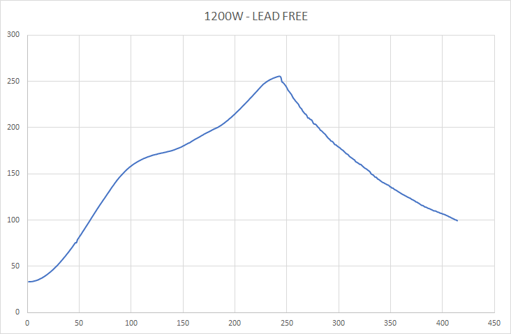
We have installed the Tiny Reflow controller v1 on our small modified oven. This was a small 600W oven with analog dials and thermostat and we added insulation and two additional heating elements of 300W each. So total power is now 1200W. This makes the oven more powerfull and it is now able to reach desired temperature easier than with the 600W heating elements. You can see the different of the 600W and 1200W performance on the following graphs.
Tiny Reflow v1 added to our 600W -> 1200W upgrated mini ovenOven was upgraded to 1200W and insulated from inside. Here you see it with the door open and temperature sensor.View of the additional bottom heating element (300W) modification and temperature sensor
Reflow Results
The Tiny Reflow provides some statistics on it’s RS-232 output. Use any serial terminal program at 115200 bps 8N1 configuration to collect the temperature information across time. Two plots of the reflow profiles are shown below. The first is before modifying and insulating the oven (600W) and the second if for the 1200W modified oven. As you can see on the second graph the total reflow time was about 415 sec while the first graph shows 500 sec. Also you can notice that the 1200W reflow profile achieved a better preheat temperatre slope than the 600W that means it reached the desired temperature more easily. The 600W oven was strungling to do.
Demo Video
Conclusion
You can go through this list curated by Rocket Stream to get suggestions on the best kind of ovens to use with the tiny reflow controller or visit their eshop to purchase an already assembled and tested board.
That’s it for today’s tutorial. Thanks for reading. As usual, feel free to reach out to me via the comment section if you have any question about the project and also let me know if you made one following this guide.
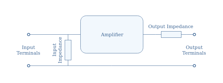
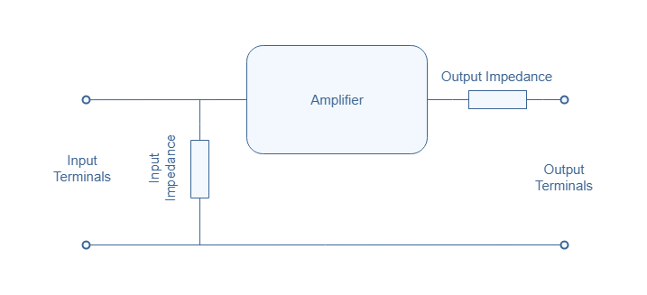
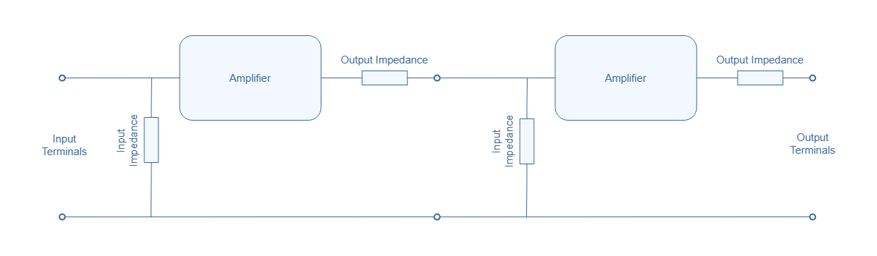
In a very simplified point of view, an amplifier consists of a “box” that realizes an amplification function between an input signal and an output signal. The way that the input enters the system and the output leaves it is very important and affects the general behavior of an amplifier. In more technical terms, the flow of current of both the input and output is controlled by the input and output impedance of the amplifier.
This tutorial clarifies the notions of input and output amplifiers impedances by explaining the previously mentioned concept of “box”. The second section highlights the several reasons of importance of choosing appropriate values for these parameters. Finally, some methods are exposed to set the amplifier’s impedances, therefore to greatly affect the circuit behavior.
Definition of the input and output impedances
First of all, it is important to realize for the understanding of this tutorial that the input and output impedances are a concept and do not represent any physical resistor that can be removed or changed. Indeed, they represent a value in Ohms (Ω) that takes into consideration the design of the amplifiers (the arrangement of the components around the transistor) and to what and how they are connected (source, other amplifiers or transducers). We will detail later on these different connection arrangements.
The input impedance is connected across the input terminals of the amplifier while the output impedance is connected in series with the amplifier. A representation of this configuration is shown in Figure 1 below :
fig 1 : Definition of the input and output impedances
If we consider the input voltage and current to be Vin and Iin and the output voltage and current to be Vout and Iout, the simplest definitions of the impedances Zin and Zout are given by :
Zin=Vin/Iin
Zout=Vout/Iout
Generally, an input impedance is high and an output impedance is low. Ideal amplifiers have an infinite input impedance and a zero value for the output impedance.
Importance of the Impedances
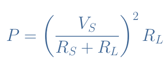
If there is something to really keep in mind about why input and output impedances are so important is matching. Impedance matching is a simple concept that states that the power transfer from an internal source resistance (RS) to a load (RL) is maximized when RS=RL. A simple representation is given below to define the different parameters in this context :
fig 2 : Maximum transferred power problem
This theorem can be proved easily through some calculation steps that involves derivative calculus. The expression of the transferred power P as a function of VS, RS and RL is given in Equation 1 below :
eq 1 : Transferred power
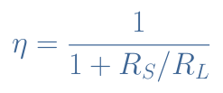
However, maximum transferred power does not imply maximum efficiency. It is indeed a common source of error since even Joule himself misunderstood it. Efficiency relates to the percentage of power that can be transferred from the source to the load, whereas the transferred power refers to the maximal magnitude of the power that the load can develop.
The formula for the efficiency satisfies Equation 2 :
eq 2 : Efficiency of the circuit
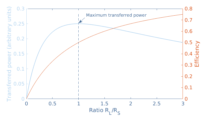
Both the transferred power and efficiency can be plotted in the same graph as a function of the ratio RL/RS :
fig 3 : Transferred power and efficiency as a function of the ratio RL/RS. Plotted with MatLab®
From Figure 3 we can indeed see that the transferred power is maximized when the impedances are matching, that is to say when RL/RS=1. For a perfect impedance match, the efficiency only reaches 50 %. A 100 % ideal efficiency is achieved when the ratio RL/RS tends to an infinite value, that is to say when RL→+∞ or RS→0 or both.
Without even considering this graph, it is indeed easy to understand that when RL>>RS, most of the power is transferred to the load since the voltage across a resistance is directly proportional to its value in Ohms. However, when the ratio RL/RS increases, so does the global resistance of the circuit and therefore the magnitude of the transferred power decreases.
On the other hand, if the load resistance is lower than the source resistance, most of the power is dissipated in the source, leading to a poor efficiency of the power transfer even if the global resistance decreases, which results in a higher magnitude of the power.
So should the impedances match to achieve a maximum transferred power or should RL>>RS to achieve maximal efficiency ?
Nowadays, as a general rule, high input and low output impedances are the norm, even if it does not lead to an impedance match. However, we will see in the next section that in some cases, impedance matching can be more suitable.
“Impedance conflicts” happens between an output and an input terminal. Basically, we can distinguish three scenarios of connection. The first one, is when a source is connected to an amplifier, this is what is shown in Figure 2.
The second case is when the amplifier is connected to a transducer. A transducer is the final stage of the circuit, it is the element that converts the electric signal into sound and movement for example, examples of transducers are loudspeakers and motors. The configuration of this connection is the same as presented in Figure 2 where the source would be the amplifier and the load the transducer.
The last scenario is the so called “cascade” configuration shown in Figure 4 where multiple amplifiers are connected to each other. In modern electronics, this type of architecture is very common to realize multiple operations and amplifications to the signals.
fig 4 : Cascade configuration
Impedance setting
In the input stage, where a power supply (source RS) is connected to an amplifier (RL), a maximum transferred power is not necessary since the amplifier can itself re amplify the signal. Usually, a signal loss of -6 dB between the source and the first amplifier (commonly known as preamplifier) is acceptable, such a loss is achieved when an impedance match is realized. Therefore, technically any ratio of output/input impedance that satisfies RL/RS>1 can be considered. Since it is never recommended to have an input impedance lower than the value of the internal source resistance, amplifier’s input resistances are high so that they can adapt to a wide variety of sources, thus to many values of source resistances..
In the case of the cascade configuration presented in Figure 4, two functioning modes can be distinguished and treated differently :
If a voltage transfer is to be realized, the output impedance of the first amplifier should be much lower than the input impedance of the next amplifier. This maximizes, such as what we described for the input stage, the voltage drop across the input impedance of the second amplifier rather than in the output impedance of the first.
If a power transfer is to be realized, it is more appropriate to match the impedances so that a maximal magnitude of the power can be transferred across several stages of amplifiers.
For the final stage, where a last amplifier supplies a transducer (lets say a loudspeaker), the output impedance of the amplifier must be lower than the internal loudspeaker resistance. Again for the same reasons, the power is transferred more efficiently to the transducer if the amplifier has a low output impedance. In this case, most of the power can be used by the transducer. However, the global resistance should not be too high to avoid a low power magnitude.
Setting methods
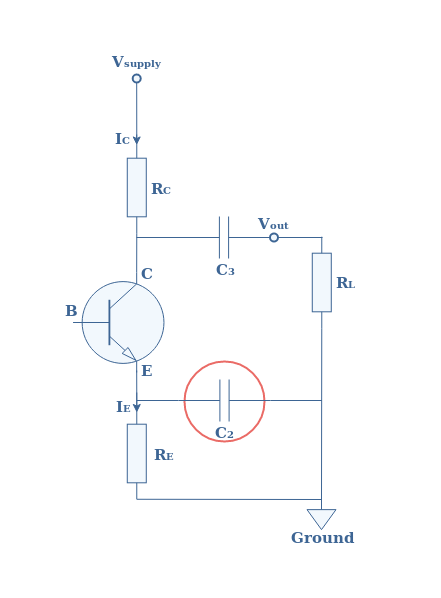
fig 5 : Focus on the decoupling capacitor
The input and output impedances values are fully given by the architecture of the amplifiers. We can list some of the architectures that are available in order to modify the input or output impedances :
FET input stage : Field Effect Transistors such as the MOSFET can be used to connect the source to the preamplifier. Since their gate is purely voltage-driven, they do no take any current at the input and thus provide a very high input resistance.
Decoupling capacitors : In the Figure 5 , a decoupling capacitor in the output stage of a Common Emitter configuration is highlighted in the red circle. In the Common Emitter Amplifier tutorial, we have already seen that using a derivation capacitance increases the gain of the amplifier. However, it also decreases the input impedance of the structure. Adjusting the value of this capacitance can therefore modify the value of the input impedance of the amplifier.
Emitter-follower : One of the easiest solution to obtain both high input and low output impedances is to use the emitter-follower configuration. Much more details of this configuration can be found in the tutorial about the Common Collector Amplifier.
Conclusion
This tutorial has first of all defined what exactly the input and output impedances are. We have seen that they represent the total resistances of the amplifier at the input terminals and at the biased output terminals. Since they do not represent any physical resistance they cannot be removed, but as a consequence of the amplifier architecture, their value can be adjusted.
These impedances play an important role at the interfaces of the amplifiers. They indeed dictate how the voltage or power signals are being transmitted from either a source to a preamplifier, from an amplifier to another amplifier or from an amplifier to a transducer.
Two criteria are mostly used in order to set the impedances : the transferred power or the efficiency. Generally, a high efficiency is preferred for voltage amplifiers. It can be achieved by setting the input impedance of the stage n+1 much higher than the output impedance of the stage n. With this configuration, despite the global resistance increasing, much of the power is developed at the n+1 stage input terminals rather than dissipated by heat losses in the output.
Sometimes however, it can be suitable to obtain a maximum of transferred power by realizing an impedance matching. In this case, the input and output impedances are set to be equal so that the power magnitude is maximal at the n+1 stage input terminals. This configuration is appreciated in power amplifier where a power transmission must be privileged.
Finally, we have seen that changing the input and output impedances must be done by modifying the architecture of the amplifier. A wide variety of configurations are indeed available, but some of the most important are given in a last section.
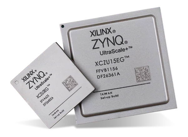
Xilinx Zynq® UltraScale+ MPSoCs Multiprocessors feature 64-bit processor scalability that combines real-time control with soft and hard engines for graphics, video, waveform, and packet processing. The multiprocessor systems-on-chip devices are built on a common real-time processor and programmable logic-equipped platform. UltraScale+ MPSoC Multiprocessors consist of three distinct variants (dual-core, quad-core, and video code-c). Dual-core application processor-equipped (CG) devices are optimal for industrial motor control and sensor fusion. Quad-core application processor-equipped (EG) devices excel in wired and wireless infrastructure, data center, and Aerospace and Defense applications. Video codec-equipped (EV) devices are ideal for multimedia, Automotive ADAS, and surveillance applications.
Features
Quad- or dual-core ARM Cortex A53 application processing unit
Dual-core ARM Cortex-R5 real-time processing unit
ARM Mali-400 MP2 graphics processing unit
Video codec unit
Xen Hypervisor enables multiple concurrent operating systems on the Cortex-A53 APU
Xilinx OpenAMP communicates and manages independent processors and software stacks
ARM-trusted firmware guarantees secure access and protect key system resources
Boot loaders manage system from power-on-reset with many advanced features including decryption and authentication