With the advent of IoT and the proliferation of connected embedded devices, one of the biggest challenges in developing competitive IoT solutions is the ability to bring intelligence at the Edge of the IoT networks. Edge computing is crucial in IoT applications as it paves the way for faster real-time inference by embedding computation capability in on-premise infrastructure resulting in a dramatic improvement in overall system reliability and performance.
With edge computing increasingly forming the foundation of next-generation secure and connected devices, it is important to highlight the significance played by the hardware accelerators in determining system performance & efficiency and therefore should be considered with utmost importance while developing edge gateway solutions.
Over the years significant advancement in FPGA technology has led to FPGAS becoming mainstream for developing intelligent edge platforms. FPGAs sophisticated performance and adaptability coupled with their ability to deliver the highest throughput at the lowest latency makes them ideal for enabling highly responsive real-time inference at the edge.
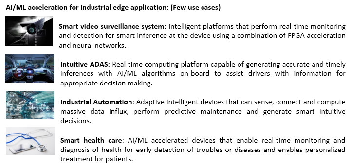
At iWave Systems, a leading FPGA design house based in Bangalore, we have expended state of the art Xilinx Zynq® UltraScale+™MPSoC FPGA modules to bring forth intelligence in edge devices using advanced AI/ML accelerations. iWave’s Zynq® UltraScale+™MPSoC FPGA SOM offers versatile hardware accelerations for intuitive deployment of functions such as, image /speech recognition, object /pose detection, etc. and a flexible platform that enables developers to continually refine features and sharpen their competitive edge. Implementing artificial neural networks in FPGAs provides the flexibility to adapt applications with changing standards and end-user demands, which in turn future proofs your designs.
Xilinx/DeePhi core platforms for AI/ML inference in iWave’s Zynq® UltraScale+™MPSoC SOM
The image shows a representation of AI/ML acceleration on iWave’s Zynq UltraScale+ MPSoC development kit using Xilinx/Deephi core platforms for object detection, human detection, pose estimation and face detection.
The Zynq UltraScale+ MPSoC SOM features an intelligent blend of MPSoC and FPGA functionality in an ARM® + Xilinx FPGA architecture that forms a highly integrated & powerful embedded platform for edge applications. The heterogeneous ARM® multicore processors complement the edge applications with high-performance non-real-time processing such as system boot, peripherals management, server communication, etc., while offloading the FPGA to execute critical real-time tasks using Deephi algorithms.
Deephi core platforms integrate both hardware and software components, presenting a comprehensive framework for AI/ML acceleration in applications such as face recognition, real-time surveillance, image / pose detection, etc. With its industry-leading AI/ML capabilities, the Xilinx/ Deephi core platform allows high-level adaptiveness to various workload characteristics and complement edge applications with ultra-low latency real-time inference.
With its support for a wide range of Neural Networks, the Xilinx/ Deephi core platforms are continuously evolving, integrating new and advanced algorithms for improved determinacy and inference in AI/ML applications. iWave supports a huge portfolio of Deephi cores enabling customers to choose from a variety of algorithms based on their application needs which allow for superior inference at edge applications. Refer the link https://www.xilinx.com/products/design-tools/ai-inference.html#models to gain insights about the various neural networks supported by Xilinx/ Deephi .
Needless to say, edge computing continues to revolutionize the IoT ecosystem with competitive applications that enable the best consumer experience. iWave’s Xilinx/Deephi platforms offers high-performance adaptive hardware acceleration for implementing AI/ML acceleration in edge applications with utmost flexibility and ease of use enabling developers to accelerate innovation and bring designs to life fast at optimized cost and lead time.
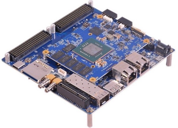
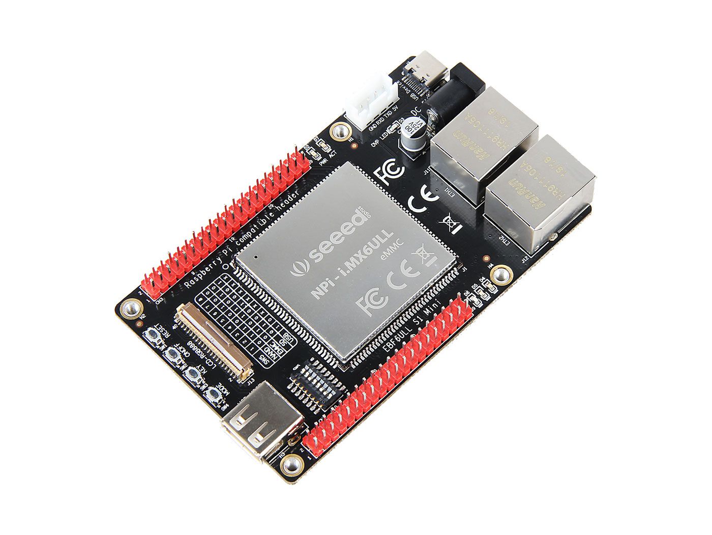
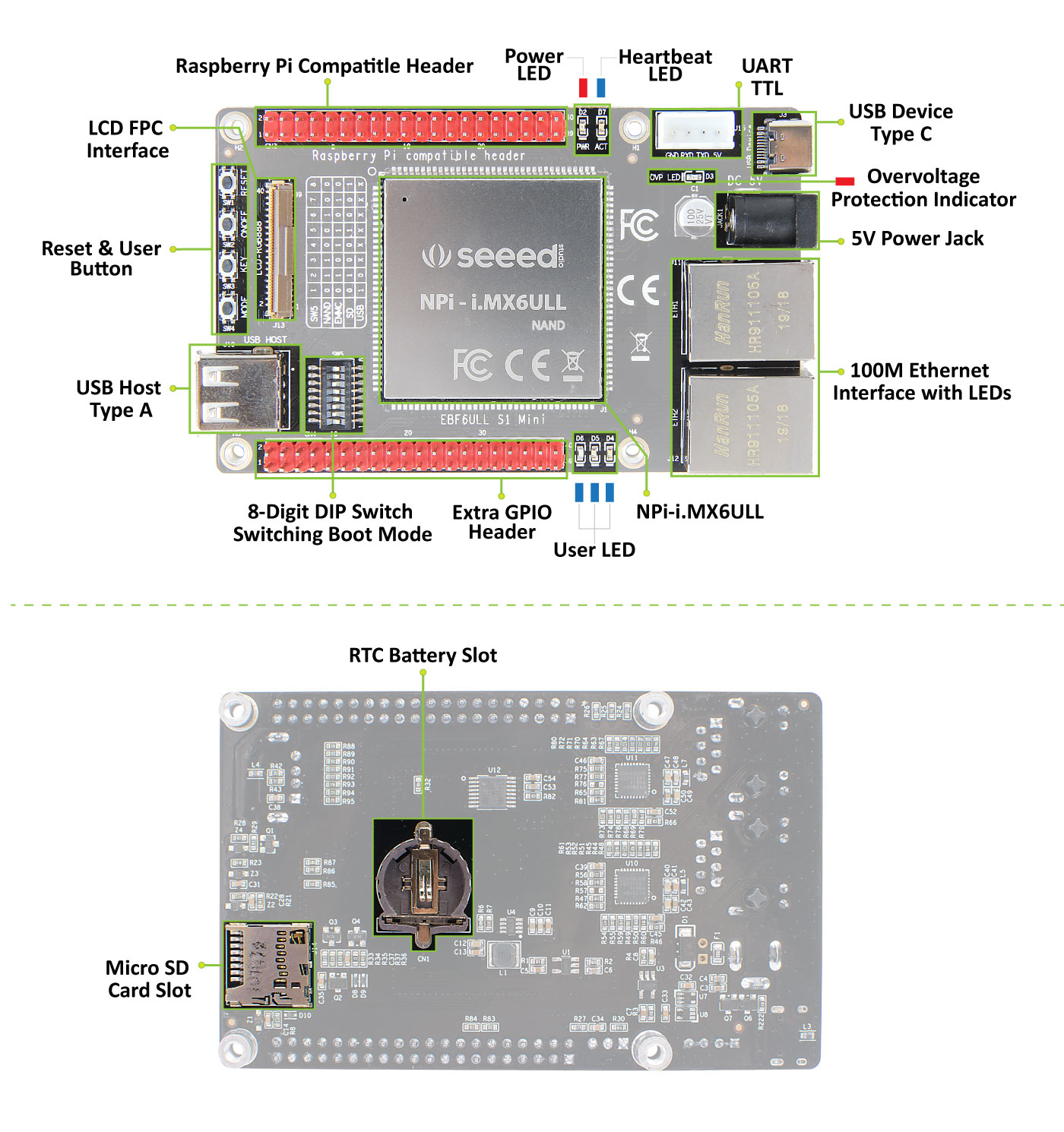
SeeedStudio recently announced that they have started taking pre-orders for their new NPi i.MX6ULL – Linux SBC Development boards. The board is a low-power, linux-based single board computer and can be referred to as essentially a breakout board on steroids for the i.MX6ULL COM (Computer-on-module) chip. It is targetted at industrial applications with several features that support industrial use cases, and board parts/components of industrial grade.
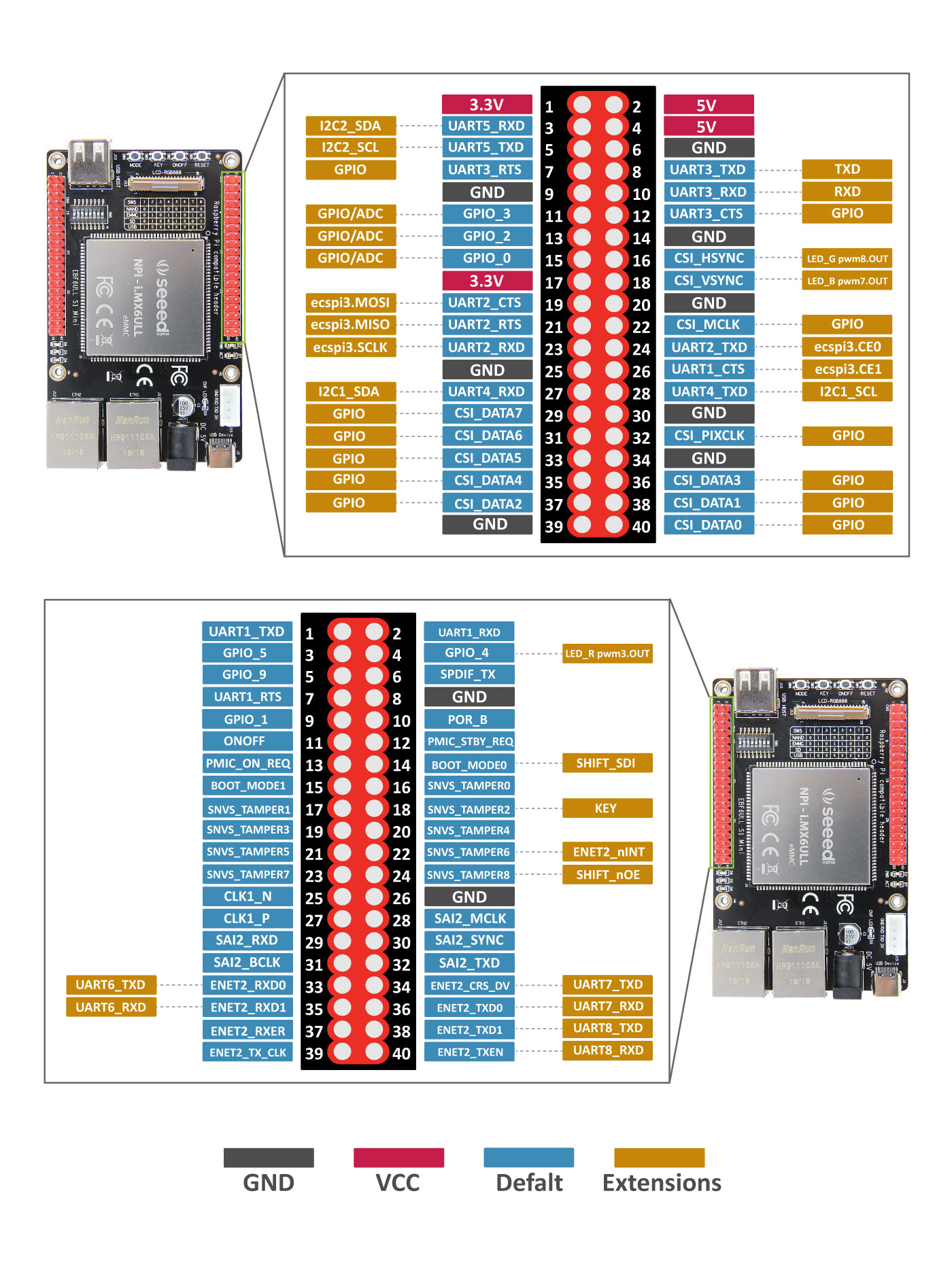
The NPi includes an NXP Arm Cortex-A7 processor running up to 800MHz, 512MB of DDRL3 RAM, with a choice of 256MB of NAND flash or 8GB of eMMC storage, and an on-board battery-backed real-time clock. On-board connectivity options includes two 100Mb Ethernet ports, a single USB 2.0 Host connection, a USB Type-C port for operation in device mode, a microSD slot for additional storage, FPC LCD interface with touch input, and two 40-pin GPIO headers.
One of the main attractions to the dev board is its compatibility with the Raspberry Pi GPIO pinout which brings the compatibility with several HATs designed for the Raspberry Pi without need for any modification to the development Board. Seeed also promised the boards will be compatible with several of their own HATs and users will be able to add features like CAN-BUS, Audio, and other connectivity options via the HATs. However, the ReSpeaker 6-Mic Circular Array Kit for Raspberry Pi and ReSpeaker 4-Mic Linear Array Kit for Raspberry Pi may not work due to the HAT configuration.
Some of the highlight features of the board include:
NXP MCIMX6Y2CVM08AB CPU
800Mhz Frequency
onboard 512MB DDR3L
onboard 8GB eMMC
-20℃ ~ 80℃ operating temperature
2 x 100M ethernet port
5V±2% DC jack
FPC LCD interface (including 24 bit RGB and I2C touch control)
In addition to these features, the board also comes with a USB Host Type A which allows USB based devices to be connected the board.
The boards are now availabe for pre-orders with shipping date as early as the end of October. The 256MB NAND version of the board is available for $39 while the 8GB eMMC version goes for $44.
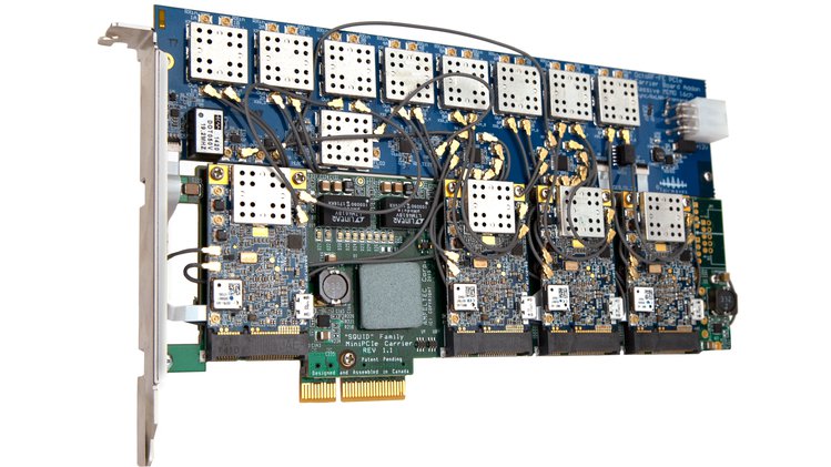
XYNX (pronounced ikz-sync) is being launched on Crowdsupply by Fairwaves. it is based on the success of the Octopack SDR (software-defined radio) and the feedback the firm received from the original Octopack users. It is designed for situations or use cases that involve large band of spectrum monitoring or massive MIMO system and it comes in four different variations including; XYNC Quadro, XYNC Quadro 6, XYNC Octo and XYNC Octo x2.
The major difference between the models is the number of XTRXs and communication channels. The XYNC Quadro and Quadro 6 both come with four XTRXs and 8×8 channels for transmitting and receiving, with the two models transmit at the same frequency range (30MHz-3.7GHz) but receive at a different frequency range (Quadro: 30MHz-3.7GHz, Quadro 6: 1.8GHz-6GHz), While the XYNC Octo and Octo x2, on the other hand, both have the same frequency range at the transmitter and receiver but a different number of the channel for transmitting and receiving (octo: 16×16 channel, octo x2: 32×32 channel) and XTRXs (for octo and octo x2 having 8 and 16 XTRXs respectively). However, two or more XYNC board can be connected together to increase the number of RX/TX channels to what you desire but requires an external clock and 1pps signal distribution circuitry to do so (e.g., two XYNC Octos give you 32 TX and 32 RX channels).
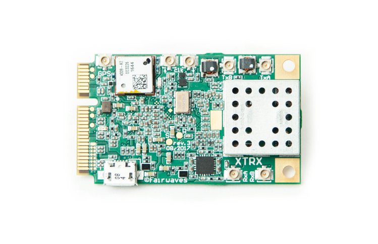
A single XTRX is shown above. XYNC includes up to eight XTRX boards.
One of the great things about the XYNC is the possibility of Synchronizing the XTRXs (which provides two transmit channels and two receive channels) which forms a single XYNC board. For instance, two XYNC Octo (with eight XTRX units) has 16 transmit and 16 receive channel each, can be synchronized and to get 32 transmit and 32 receive channels. All XYNC are equipped with a special board to facilitate this synchronization of the XTRX units along with cables for all of the TX/RX ports, the GPS port, and metal installation brackets.
Due to the possibilities of synchronizing, the maximum achievable RF bandwidth is a function of the individual XTRX RF bandwidths since XYNC is based on multiples of the synchronized XTRX SDRs.
On the digital side, each XTRX unit is connected to a PCIe switch which multiplexes the XTRX PCIe lanes into a single PCIe 2.0 x4 connector. This makes it easy to install into a standard PC in a very compact way – just don’t forget to provide enough airflow for cooling, as it can get quite hot.
A summary of some of the fascinating general features of the XYNC include;
RF Chipset: 4x or 8x Lime Microsystems LMS7002M FPRF
Channels: 8×8/16×16/32×32 MIMO depending on the board type
Full-size PCIe form factor
Rx/Tx Range: 10 MHz – 3.7 GHz or 100 kHz – 3.8 GHz with signal level degradation
RF Bandwidth: 1.4 MHz to 130 MHz (1.4 MHz to 30 MHz for the 6 GHz Rx option)
FPGA: 4x or 8x Xilinx Artix 7 50T
Sample Rate: ~0.2 MSPS to 120 MSPS per channel
PCIe x4 Gen 2.0, 16 Gbit/s PCIe Bandwidth
0 to 10 dBm RF Output Power (depending on the frequency)
30 MHz – 3.8 GHz Tunning Range
<10 µs Bus Latency (stable over time)
While there is currently no price tag mentioned in the description, it can be assumed that it will be more expensive than the XTRX and judging by how well supported the campaign for the XTRX was, it’s probably okay to believe enough funds will be raised to being the XYNC to reality. More information about the project can be found on the CrowdSupply project page.
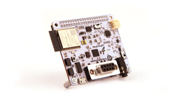
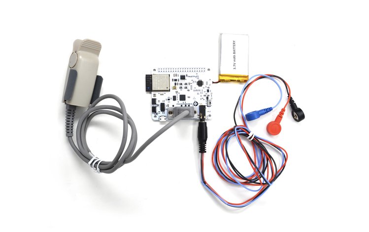
Following the success of their HealthyPI V3, ProtoCentral has launched a CrowdSupply campaign for an upgrade to the HealthyPi V3 simple called the HealthyPi v4. The HealthyPi V4 just like the V3 is a vital signs monitoring dev kit, that provide users with the opportunity to monitor parameters like the body temperature, oxygen saturation, and ECG/respiratory data. It is based on the Raspberry Pi like it’s predecessor but is however designed as a wearable device with wireless capabilities to solve the need of keeping users tethered to a machine round the clock so as to monitor vital signs.
According to ProtoCentral, one of the main inspiration behind the HealthyPi V4 was the desire to solve the problem of round the clock tethering to machines that people have to go through for their health to be monitored in a realiable way. To achieve this, the HealthyPi V4 comes with a simple physical switch which can be used to toggle between continuous mode, for use as a Raspberry Pi HAT, and wearable mode, which allows HealthyPi v4 to function as a standalone unit.
Irrespective of the mode, the HealthyPi v4 measures important parameters like:
Electrocardiogram (ECG) data, heart rate, and heart-rate variability
Respiration based on an impedance pneumograph
Pulse oximetry (SPO₂)
Body temperature
All of these parameters are monitored in real – time and and at high accuracy which opens the device up to use by different categories of people including researchers, makers and everyday users. The connected nature of the device also makes it invaluable and expands the use case as far as remote patient monitoring in regions where access to the health facilities is low.
HealthyPi v4 was designed to allow vitals monitoring in 2 ways:
Via the Android App
Using the Web Server Mode
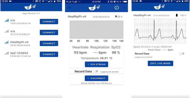
The Android App was designed to simplify the process of viral monitoring. You only need to download the app from Playstore, connect it to the HealthyPi v4 device via BLE. Immediately your phone’s bluetooth comes on, you should see the device home page with a place for you to select the device. Immediately the selection is done, you should see the heart rate, respiration rate, temperature and SpO₂ levels displayed with an additional screen to render real-time ECG waveform.
HealthyPi V4 Android App Screens
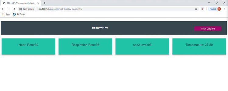
The webserver mode, on the other hand, allows you to stream live data over the local network. Simply push a button while starting up the device, and it will enter Wi-Fi Access Point (AP) mode. You can then connect to the “HealthyPi” Wi-Fi network using your computer or mobile device and point your browser to http://Healthypi.local. The HealthyPi home page will display live vitals as well as plots. This page also provides Over-The-Air (OTA) software and firmware updates.
HealthyPi V4 Webserver Interface
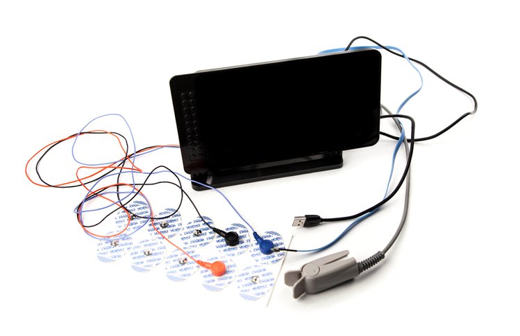
Asides these two ways, HealthyPi v4 also maintains full compatibility with HealthyPi v3 through its continuous mode, which streams real-time data to a Processing-based application that is compatible with Raspberry Pi devices and desktop platforms (including Mac, Windows, and Linux). Upon successful connection, ECG, respiration, and PPG data will be displayed along with computed heart rate, respiration rate, SpO₂, and temperature readings
A highlight of the features of the HealthyPi v4 includes:
ESP32, in WROOM32 module format, with a Dual-core Xtensa 32-bit CPU, 4 MB of on-board flash, Wi-Fi, and support for BLE
Wi-Fi and Access Point (AP) modes, a 2.4 GHz radio with an on-board PCB antenna that is compatible with Bluetooth 4.2 and BLE
Supports Arduino IDE as well as Espressif ESP-ID
Texas Instruments (TI) ADS1292R 24-bit analog front end with signal-to-noise ratio (SNR) of 107 dB for ECG and respiration front end:
TI AFE4400 pulse oximetry front end with integrated LED driver and 22-bit ADC
Maxim MAX30208 digital body temperature sensor for monitoring skin temperature
Raspberry Pi HAT form factor (65 mm X 56 mm)
Comes with a 40-pin standard HAT-compatible headers for connecting to any Raspberry Pi
2x Qwiic connectors to enable connection to any Qwiic-compatible board for virtually limetless I²C sensor modularity
On-board USB-to-UART converter for programming and data transfer
Easily transition between wearable mode and HAT mode
HealthyPi v4 ships with firmware that enables all of this functionality out-of-the-box. If you want to make changes to the firmware, however, you will find the Arduino IDE – which is compatible with Mac, Windows, and Linux – easy-to-use for beginners but flexible enough for advanced users. In addition to Arduino IDE, HealthyPi v4 also supports Espressif IDF, so you can code in whichever environment you prefer.
HealthyPi V4 Complete Kit
While no price tag has been placed on the device yet, the Crowd Supply campaign states that the HealthyPi v4 will be avaialable as a HAT kit or a complete Kit. The hat kit will contain; the HealthyPi v4 main board, a 1000 mAh battery, three-electrode cable with ECG “snap connectors” on one end and a stereo connector on the other, Sheet of 20 single-use ECG electrodes, Finger-clip SpO₂ probe with a Nellcor-compatible DB9 connector, Qwiic-based temperature sensor, and the HAT mounting kit with headers and screws for stacking atop a Raspberry Pi. The complete Kit on the other hand will include everything in the HAT Kit along with; a Raspberry Pi 3 Model B+ computer, 16 GB microSD card with Raspbian and HealthyPi software, an official, 7” Raspberry Pi touchscreen LCD display, SmartiPi Touch enclosure for the Pi and the display, and an Isolated, medical-grade (5 V, 2.5 A) USB wall power adapter (100-240 VAC) with snap-on plugs for the following regions: US, EU, UK, and AU.
A few years back, Microchip/Atmel announced the release of a completely new range of chips designed to serve as replacements for their older ATmega and ATtiny ranges. The new ATtiny chips started with the 1-series which included ATtiny417 and ATtiny817, which was followed in 2018 by the cheaper 0-series microcontrollers which included microcontrollers like the ATtiny1604 and ATtiny402. The new range of microcontrollers now comprises of a total of 25 parts. However, for makers, DIY Hobbyists and fans of the Arduino development platform, it was not a celebration as there was no support to enable programming of the mcus using the Arduino IDE. This however changed some months ago when the megaTinyCorewas released as an Arduino core to support programming of the new range of Atmel microcontrollers. For today’s tutorial, we will look at the process of using the megaTinyCore to program one of these new ATtiny microcontrollers using the Arduino IDE.
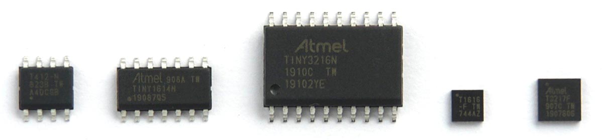
A selection of the new ATtiny chips: SOIC ATtiny412, ATTiny1614, and ATtiny3216; QFN ATtiny1616 and ATtiny3217. (image: technoblogy.com)
The MegaTinyCore is an Arduino core for programming the new series of Microchip microcontrollers with the Arduino IDE. The Core is based on the work done by the Arduino team during the development of support for their new ATmega4809-based boards. While the core provided everything we needed to compile code for the new microchip series boards, there was still a slight problem as the ATtiny 0- and 1-series can only be programmed through a Unified Program and Debug Interface (UPDI) (a 1-wire interface using the reset pin on the ATtiny) because they do not have a bootloader, and as such cannot be programmed via ISP or with ISP programmers. To solve this problem, GitHub user ElTangas wrote a UPDI programmer which can be uploaded to an Arduino Uno or equivalent board to turn the board into a UPDI programmer for the new series board, giving users the ability to not only develop their code with the Arduino IDE, but also upload the code to their target microcontroller using the Arduino board as the programmer, totally eliminating the need for Atmel studio in the development process.
Based on the above, this tutorial will show how you how to set up an Arduino board as the UPDI Programmer and the process of setting up the megaTinyCore on your Arduino IDE.
Required Components
The following components will be needed to follow this tutorial:
Attiny412
An Arduino Uno or nano
Adafruit 8-pin SOIC
4.7k Resistor
1ouf Capacitor
Breadboard
Jumper Wires
None of the new ATtiny devices are available in DIP packages, as such, to connect them on a breadboard, you will need a sort of breakout board which is why the Adafruit 8-pin SOIC is being used for. For microcontrollers with more pins, you can check out their 14 and 20 pin SOIC or these 24-pin VQFN board on Amazon. All of these components can be bought from the majority of online electronics component stores.
With all the components in place, we can start by Installing the megaTinyCore on the Arduino IDE.
Installing the MegaTinyCore
The megaTinyCore requires Arduino IDE version 1.6.3 or later although it was stated on its GitHub page that it may require a much more recent version of the IDE but the initial test was done with version 1.8.9.
The megaTinyCore can be installed on the Arduino IDE in two ways;
Installation via the Arduino Board Manager
Manual Installation
I will explore both methods and let you decide which is easiest or faster.
1. Installation via the Arduino Board Manager
The Arduino board manager was designed to make the installation of new boards and add-ons easy for users. To install the megaTinyCore using this method, follow the steps enumerated below;
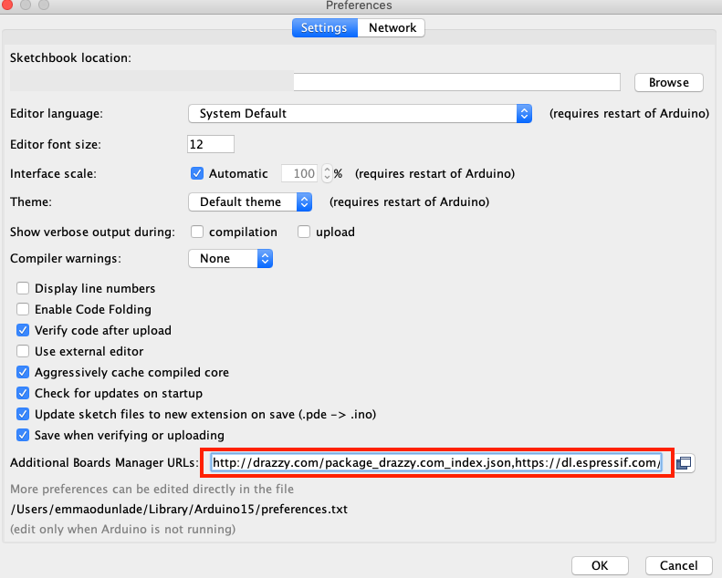
Open the preferences window from the Arduino IDE. Go to File > Preferences or Arduino > Preferences if working from a macOS
On the preferences window, locate the “Additional Board Manager URLs” text box and enter http://drazzy.com/package_drazzy.com_index.json into the field as shown below and click the OK button
Add the Link to Additional Board URL List
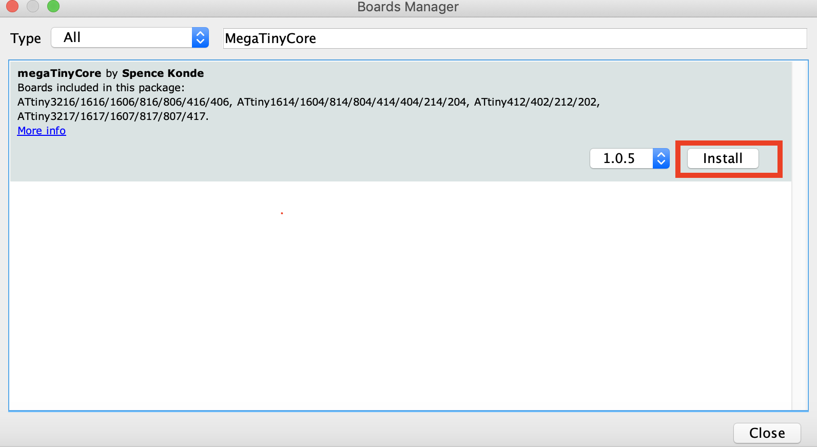
Next, open the Arduino board manager. Go to tools>Boards>Boards manager
When the board manager opens up, enter megaTinyCore into the search bar and scroll, you will see “megaTinyCore by Spence Konde”, click on install as shown below.
Also, search for the “Official Arduino megaAVR boards” package and install the most recent version of that too.
With all of that done successfully, you should now see the Attiny boards all listed under the boards’ section (tools -> Boards) of the Arduino IDE. If that is so, it means the board installation was successful.
2. Manual Installation
The Arduino board manager method provides some level of automation while the manual installation, on the other hand, allows the latest version of the core to be installed, with fixes that may not yet be available in the board manager version of the core. However, to use the manual installation, it is required that you use board manager to install the latest version of the Official Arduino megaAVR board package for manual installation to work.
Manual installation is recommended if you are interested in contributing to the development of the core, or if having the latest fixes which are not in the released version is important to your build.
To install manually, follow the steps below;
Ensure you have installed the latest version of the Official Arduino megaAVR board package.
Download the MegaTinyCore.zip package (either the “released” version or by downloading the .zip of the master repo) on your computer.
Extract, and place the file in the “hardware” folder inside your sketchbook folder (where your Arduino Sketches are saved). If the hardware folder does not exist, create a new folder and name it “hardware”.
Restart the Arduino IDE
For automatic updates, instead of downloading the zip file, you can download the GitHub client, and sync this repo to the hardware subfolder of your sketchbook folder.
With the installation steps completed, you should now see the Attiny boards all listed under the boards’ section (tools -> Boards) of the Arduino IDE if the installation process was successful.
With that done, the next step is to set up a UPDI programmer after which you will be ready to upload code to any of the new attiny series Microchip microcontrollers.
Make the UPDI Programmer
As mentioned during the introduction we will need to make a UPDI programmer to be able to upload code to the attiny series using the IDE and an Arduino board.
There are two steps to doing this. The first step involves transforming an Arduino board to serve as the UPDI programmer while the second part shows how to connect the Attiny to the programmer and the Upload process.
1. Transform an Arduino to a UPDI programmer
To transform our Arduino board to a UPDI programmer, we will use the UPDI Arduino sketch created by ElTangas. The sketch converts ATmega328(p)-based Arduino’s, like the Arduino UNO, Nano, and Pro mini, into a UPDI programmer. The sketch, however, does not work on boards based on other microcontrollers, like the 32u4 (on Arduino Micro/Leo) or any non-AVR board.
The following steps show how to make this cheap UPDI programmer;
Close all instances of the Arduino IDE to avoid errors.
Open the jtag2updi folder after extracting the download
Open the sketch jtag2updi.ino and upload it to the Arduino board you will like to use which for our sake is an Arduino Nano. When you open the code, the .ino file will appear empty and that is fine as all the code is contained in the other files in the same folder as the .ino, but the empty .ino is needed so they can be compiled by the IDE.
With upload successful, you are now ready to use the UPDI programmer. If you use the new ATtiny series a lot, it will be a smart move to totally dedicate an Arduino pro mini or nano board as a permanent UPDI programmer.
2. Connecting the Attiny and uploading
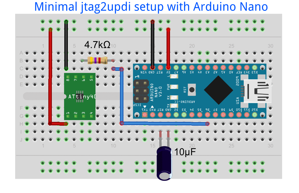
Connect the ATiny to the Arduino as shown in the schematics below;
Schematic for Connecting the UPDI programmer to the Attiny
The connection is quite straightforward but pin-pin connection between the Arduino and the Attiny is illustrated below to prevent mistakes;
Arduino Nano – Attiny
GND - GND
5V - VCC
D6 - UPDI
It is important to note that the UPDI pin of the ATiny is Connected to the Arduino via a 4.7k resistor which may not be necessary if using some of the breakout boards, as some of them come with the resistor built-in.
With the microcontroller connected to your Arduino UPDI programmer, we are now ready to upload code to the attiny.
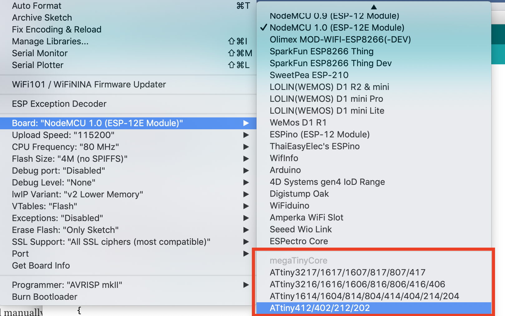
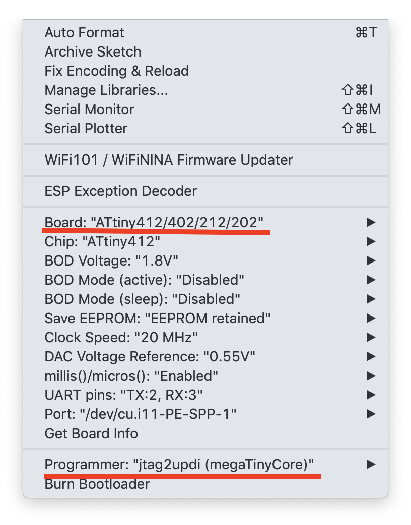
Open or write the code you would like to upload. Verify the code to ensure that there is no error, then go to Tools -> Board, and scroll down till you see the ATtiny you are working with on the list and select it.
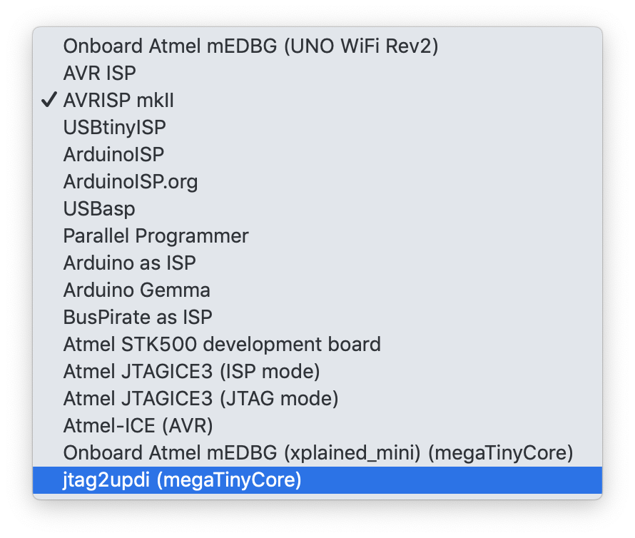
This should update the parameters being displayed when you click tools. Now we need to tell the Arduino IDE to use our programmer. To do this, go to Tools->Programmers (towards the end).
Scroll down on the pane and select jtag2updi (megaTinycore) as your programmer.
With that done, your screen should now look like the image below when you click on tools;
This means all lights are green. Now select the port to which the Arduino nano is connected and hit the upload button on the IDE. You should immediately see the upload process and when complete, the microcontroller should perform as programmed.
Compared to the former ATtiny microcontrollers, these new series of MCUs come with higher amount of flash memories, cost a whole lot less and are all-round more efficient compared to the previous set as such they should probably be considered when next you are making the choice of a tiny low-cost, low-power microcontroller for your project.
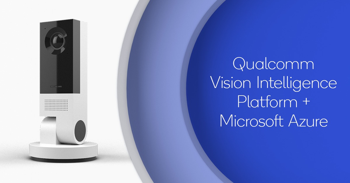
Microsoft has announced a $249 “Vision AI Developer Kit, aimed at AI edge developers using Azure IoT Edge and Azure Machine Learning. The kit features an 8MP, 4K camera which runs Linux on Qualcomm’s 10nm, AI-enabled QCS603 SoC. The Vision AI Developer Kit incorporates Qualcomm’s Vision Intelligence Platform, which is infused into its QCS603 SoC, with Microsoft’s Azure IoT Edge service, built on the Azure IoT Hub. The platform also includes Vision Studio and Azure Machine Learning (AML) for building, training, and deploying machine learning models. The kit is manufactured by Altek, and which also makes a Linux-driven, QCS603-based IPC603 camera reference design based on the QCS603.
The Vision AI Developer Kit is labeled as an “end-to-end Azure enabled solution with real-time image processing locally on the edge device, and model training and management on Azure.” Microsoft says that the kit enables you “deploy vision models at the intelligent edge in minutes, regardless of your current machine learning skill level.”
Azure provides three development paths: “no-code” using Custom Vision; Azure Cognitive Service, custom models with Azure Machine Learning; and the Visual Studio Code IDE. Targeted at novices, Custom Vision assists users through the process of uploading data, training, and deploying customer vision models including image tagging. The Vision AI Developer Kit, allows users to use Azure IoT Hub to deploy a custom vision model directly to the kit.
For more advanced users, you can try the Azure Cognitive Service with visual drag and drop tools for AML development, and also use the kit’s extension for Visual Studio Code, which offers sample Python modules, pre-built Azure IoT deployment configurations, and Dockerfiles for container creation and deployment. The Visual Studio Code also helps in adding business logic to existing Azure solutions based on camera input sent through Azure IoT Hub to transform the image data into normalized data streams using Azure Stream Analytics. The quad-core QCS603 on the Microsoft kit offers only 2x of the 1.7GHz “Silver” cores instead of six. The chips are part of the Qualcomm AI Engine built around Qualcomm’s Snapdragon Neural Processing Engine (NPE) software framework, that enables analysis, optimization, and debugging tools for developing with Tensorflow, Caffe, and Caffe2 frameworks. The Vision AI Developer Kit is built around Qualcomm’s Altek-built Vision Intelligence 300 Platform, also known as the EIC MS Vision 500 smart camera.
The device complements the Yocto Linux driven QCS603 SoC with 4GB LPDDR4. Storage option includes 16GB eMMC and a microSD slot. The centerpiece of the device is an 8-megapixel camera that features 4K UHD support and a four-microphone array. The device is also equipped with dual-band 802.11b/g/n radio, audio I/O jacks, an HDMI port, and LEDs. Power features include a USB Type-C port and a 1550mAh battery. The base of the device can swivel, enabling it has multiple mounting options.
The eInfochips/Altek Vision AI Developer Kit is available for $249 on here-Arrow shopping page. More information can be found in Microsoft’s Vision AI Developer Kit shipment announcement, and also the product page and GitHub page. Visit Altek’s own product page also for the kit.
Automotive lighting as an important safety and popular design feature in vehicles has evolved rapidly in the past years. Now, Nichia Corporation and Infineon Technologies AG (FSE: IFX / OTCQX: IFNNY) start a collaboration to add further momentum to this evolution. Together, they are developing a high-definition (HD) light engine with more than 16,000 micro-LEDs for front light applications. Unlike current HD solutions, the new device will provide high resolution light to the entire field of view of the driver.
“Our new LED matrix light will offer a resolution about 180 times as high as that of comparable solutions on the road today,” said Kanji Bando, Head of the Advanced R&D Center at Nichia. “This will pave the way for new and improved safety features and enhance driving comfort.”
For example, HD light can be used to warn the driver of hazards by highlighting people or objects on the roadside. It can project markings on the road – for example, in order to help the driver navigate through a construction site. And established features such as the glare-free high beam or bending lights run more precisely and smoothly.
The new HD light engine will employ micro-LED technology from Nichia and a new driver IC from Infineon.
“Our chip will control and diagnose all 16,000 micro-LEDs individually,” said Andreas Doll, Vice President and General Manager of the Body Power Business Unit of Infineon’s Automotive Division. “In addition to the safety benefits, our new solution will also significantly increase energy efficiency because it allows us to turn on only those LEDs actually needed for a light pattern.”
Current micro-mirrors solutions turn on all LEDs and deflect surplus light.
The new HD light can also contribute to reducing design and production complexity for car manufacturers. At the same time it increases the driver’s ease-of-use. Left-hand and right-hand drive configurations have different lighting requirements, for example. With the new HD light engine, the necessary adaptions could be programmed digitally in the factory or activated by the driver as a function on demand.
Availability
The production launch of the new HD light engine is planned for 2023 as part of Nichia’s automotive LED and laser portfolio.
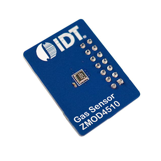
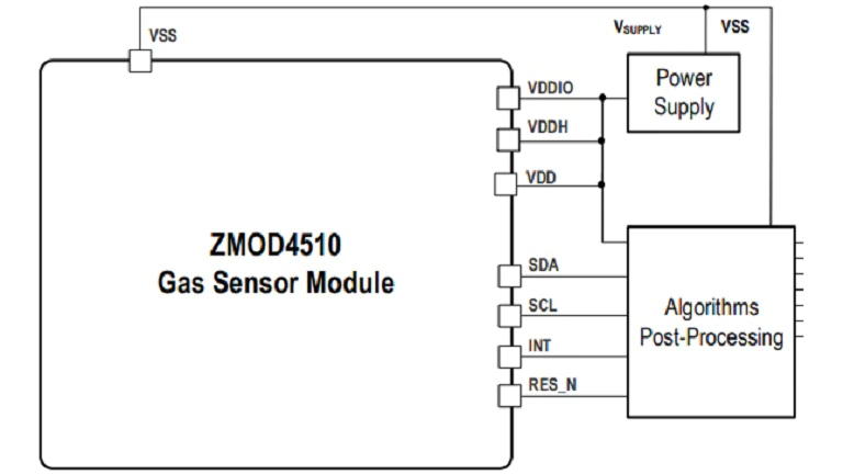
Renesas offers Outdoor Air Quality (OAQ) sensors that are calibrated to detect specific gases that contribute to unhealthy air quality
Renesas offers Outdoor Air Quality (OAQ) sensors that are calibrated to detect specific gases that contribute to unhealthy air quality, such as ozone (O3) and nitrogen oxides (NOx). By measuring these gases and using a rating scale to define levels of air quality, these sensors provide vital information that helps systems efficiently manage smart air handling systems in buildings, factories, and the home.
Key features
Reliable Detection of Outdoor Air Quality, Based on Nitrogen Oxides (NOx) and Ozone (O3)
Correlates with US Environmental Protection Agency (EPA) Air Quality Index (AQI)
Proven MOx Material with 15 Years Experience
Electrical and Gas Calibrated for Guarantee a lot-to-lot Consistency
Additional features
High Sensitivity and Long Term Stability Allows < 20 ppb Detection Limits of Ozone (O3) and Nitrogen Dioxide (NO2)
The Smallest Sensor in the Market Enables Reduced End Product Size
Allows Improved Energy Efficiency without Compromising Air Quality
Enables Rapid Customer Integration with Easy to Use Precompiled Software
Infineon Technologies introduces the new OptiMOS™ IR3826(A)M integrated point-of-load DC-DC voltage regulator. It is a fully integrated and highly efficient device in two versions (IR3826AM for 16 A and IR3826M for 23 A) for applications such as netcom router and switches, datacom, telecom base stations, server and enterprise storage.
The voltage regulator can operate from an input voltage of 12 V (5 V to 17 V) and provide up to 16 A or 23 A continuous current. It enables high-switching-frequency operations with enhanced efficiency and reduced power losses compared to previous generations of Infineon’s offering. Furthermore, the device supports high switching frequency of up to 1.5 MHz for small PCB size and less capacitors.
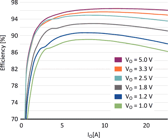
The IR3826 efficiency vs. output current. VIN = 12 V, FSW = 600 kHz, natural convection, TA = 25 °C.
Both current ratings are offered in PQFN package with 5 mm × 6 mm footprint for easy scalability. Parts are pin-compatible to the previous product offerings to allow risk-free efficiency upgrade with minimum design effort.
The IR3826(A)M solves the heat challenge without or with minimum airflow in thermally constrained application designs such us 3.3 V or 5 V supply voltages. Additionally, it supports applications that operate with high ambient temperature, e.g., 85 °C for telecom.
The state-of-the-art PWM Gen 3 engine of the devices allows operation with fixed frequency to reduce noise in multi-rail telecom or high-end Netcom applications, like base stations.
The devices are fully RoHS2 compliant without an exemption to accommodate future regulations.
Availability
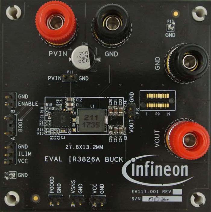
High volume production has started. Evaluation boards are also available.
Texas Instruments’ power-path management solution features 20 mA termination and 1 A boost operation
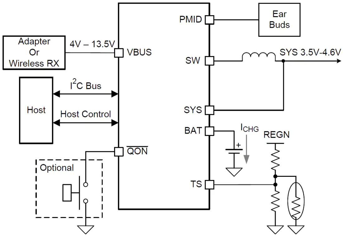
Texas Instruments’ BQ25619 integrates charge, a boost converter, and voltage protection in a single device. It offers ultra-low termination current for switching chargers to charge wearable devices by full-battery capacity. The BQ25619 low quiescent current reduces battery leakage to 6 µA in ship-mode, which conserves battery energy to double the device’s shelf life. The device is a highly integrated 1.5 A switch-mode battery charge management and system power-path management device for Li-Ion and Li-polymer batteries. It features fast charging with high input voltage support for a wide range of applications including wearables and earphone charging cases. The low impedance power-path optimizes switch-mode operation efficiency, reduces battery charging time, and extends battery run-time during the discharging phase. The input voltage and current regulation, low termination current, and battery remote sensing deliver maximum charging power to the battery. The solution is highly integrated with input reverse-blocking FET (RBFET, Q1), high-side switching FET (HSFET, Q2), low-side switching FET (LSFET, Q3), and battery FET (BATFET, Q4) between the system and battery. A bootstrap diode is integrated for the high-side gate drive to simplify the system design. The I2C serial interface with charging and system settings makes the device a truly flexible solution.
The BQ25619 supports a wide range of input sources, including a standard USB host port, USB charging port, USB-compliant high voltage adapter, and wireless power. The charger is compliant with USB 2.0 and USB 3.0 power specs with input current and voltage regulation. The device takes the result from a detection circuit in the system, such as a USB PHY device. The BQ25619 integrates a buck charger and boost regulator into one solution with a single inductor. The boost-mode supplies 5 V (adjustable 4.6 V / 4.75 V / 5 V / 5.15 V) on the PMID-pin and is used to save BOM and charge another battery by the control of PMID_GOOD. The PMID_GOOD pin is used to drive the external PMOS FET to disconnect boost output PMID from the attached accessories. The power-path management regulates the system slightly above battery voltage but does not drop below the 3.5 V minimum system voltage (programmable) with the adapter applied. With this feature, the system maintains operation when the battery is completely depleted or removed. When the input current limit or voltage limit is reached, the power path management automatically reduces the charge current. As the system load continues to increase, the battery starts to discharge the battery until the system power requirement is met. This supplement-mode prevents overloading the input source.
Features
Single-chip solution to charge wearable accessories from an adapter or battery
Single input supports USB, high-voltage adapter, or wireless power
Narrow VDC (NVDC) power-path management
Flexible I2C configuration and autonomous charging for optimal system performance
High integration includes MOSFETs, current-sensing, and loop compensation
Low RDS(ON) 19.5 mΩ BATFET minimizes charging loss and extends battery run-time
Low battery leakage current in ship-mode (7 µA), system standby (9.5 µA)
High accuracy battery charging profile
Applications
Consumer wearables, smartwatches
Personal care and fitness
Headsets/headphones
Earbuds (true wireless or TWS) charging cases
Hearing aids charging cases
The BQ25619 initiates and completes a charging cycle without software control. It senses the battery voltage and charges the battery in three phases, including pre-conditioning, constant current, and constant voltage. At the end of the charging cycle, the charger automatically terminates when the charge current is below a preset limit, and the battery voltage is higher than the recharge threshold. If the fully charged battery falls below the recharge threshold, the charger automatically starts another charging cycle. The charger provides various safety features for battery charging and system operations including battery negative temperature coefficient thermistor monitoring, charging safety timer, and overvoltage and overcurrent protections. Thermal regulation reduces charge current when the junction temperature exceeds +110°C. The status register reports the charging status and fault conditions. With I2C, the VBUS_GD bit indicates if a good power source is present, and the INT output immediately notifies the host when a fault occurs. The device provides the QON pin for BATFET enable and reset control to exit low power ship-mode or full system reset function. The BQ2619 device is available in a 24-pin, 4 mm × 4 mm x 0.75 mm thin WQFN package for easy layout.