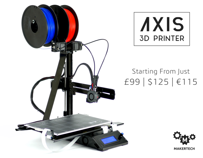
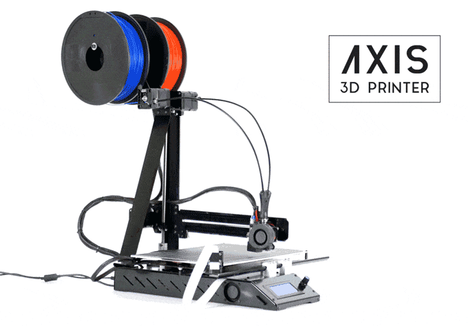
The AXIS 3D Printer is one of the most affordable 3D Printers ever made and perfect for anyone keen to dive into the futuristic world of desktop 3D Printing, without having to break the bank!
Our printer is based on open-source technology with tried and tested industry standard components designed to work right, first time.
The £99 price was achieved by creating a design that merged together the motion system and frame of the printer whilst keeping the part count to a minimum. This way we can offer high quality components but for a far lower price.
It’s worth mentioning that our margins are low, so we need your support to order large enough quantities to make the AXIS 3D Printer a success – but we will deliver and our pledge goal is very realistic for doing so!
Use the AXIS 3D Printer to print virtually any plastic object from toys and models to more practical items ranging from bike grips to shower heads! Explore the full range of possibilities on the popular model sharing site myminifactory.com.
Or take things further with the free and easy to use design software TinkerCAD to print your own unique objects!
Intro Video
The project is live on kickstarter for $125 with 33 days to go. This is an affordable 3D printer with astonish printing quality.
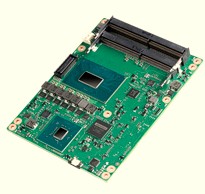
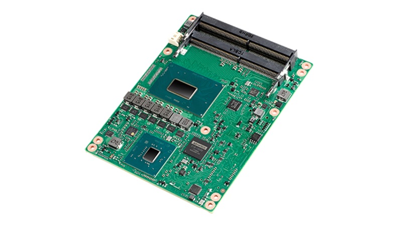
Advantech, a world leader in embedded IoT, is pleased to announce the launch of its high-end SOM-5899 series COM Express Type 6 Module designed with 8th and 9th Gen Intel® Core™ H-series processors. Compared with previous generations, the SOM-5899 is enhanced with six cores for better multithreaded performance in compute-intensive applications.
With a dual channel 96GB ECC and non-ECC DDR4 memory design, SOM-5899 increases memory capacity and bandwidth to enhance data transmission ability. The brand-new series offers multiple high-speed I/O: three ports with independent 4K displays, four ports with USB3.1 Gen 2 (10Gbps), and four ports with SATA Gen3. SOM-5899 is optimal for an array of applications, including industrial control, digital signage, automation, gaming, and medical.
Excellent Computing Power for Performance-Driven Applications
SOM-5899 provides a variety of scalable options for different power consumption and performance requirements. With its full spectrum SKUs and two-to-six core processors offering 25~45W thermal design power, customers can easily find the target SKU to fulfil system design. For extreme performance, Advantech offers the DHCS a high-end thermal solution for SOM-5899.
Enhanced Data Stability and Capacity
To meet the growing need for big data transfer and analysis, SOM-5899 comes equipped with up to 96G memory and ECC RAM. This is particularly essential in fields like medical applications, where the prevention of data loss and errors are top priorities. SOM-5899 accelerates ultra sound image processing.
Ultimate Graphics for High-Quality Visual Experience
Integrated with Gen 9.5 Intel Graphics engine, customers benefit from an enhanced visual experience and high definition media capacity. SOM-5899 supports three independent displays, offering various interfaces: VGA, LVDS for legacy applications, and three DDI ports that are configurable as HDMI/DVI/DisplayPort, for enriched visual and image focus. Ideal for medical applications, the 4K displays enhance the quality of images displayed on the Ultrasound and provides clearer pictures to both doctors and patients.
High Speed I/O for Faster Data Transmission
SOM-5899 supports four USB3.1 Gen 2(10Gbps), PEG x16 & 8* PCIe Gen3 (8Gbps), and four SATA Gen3. The flexible I/O design prepares the COM Express module for various applications in different fields such as medical, servers, and gaming. USB3.1 Gen2 doubles the speed of data transfer compared to previous generation products—saving time on the transfer of images, video, and data.
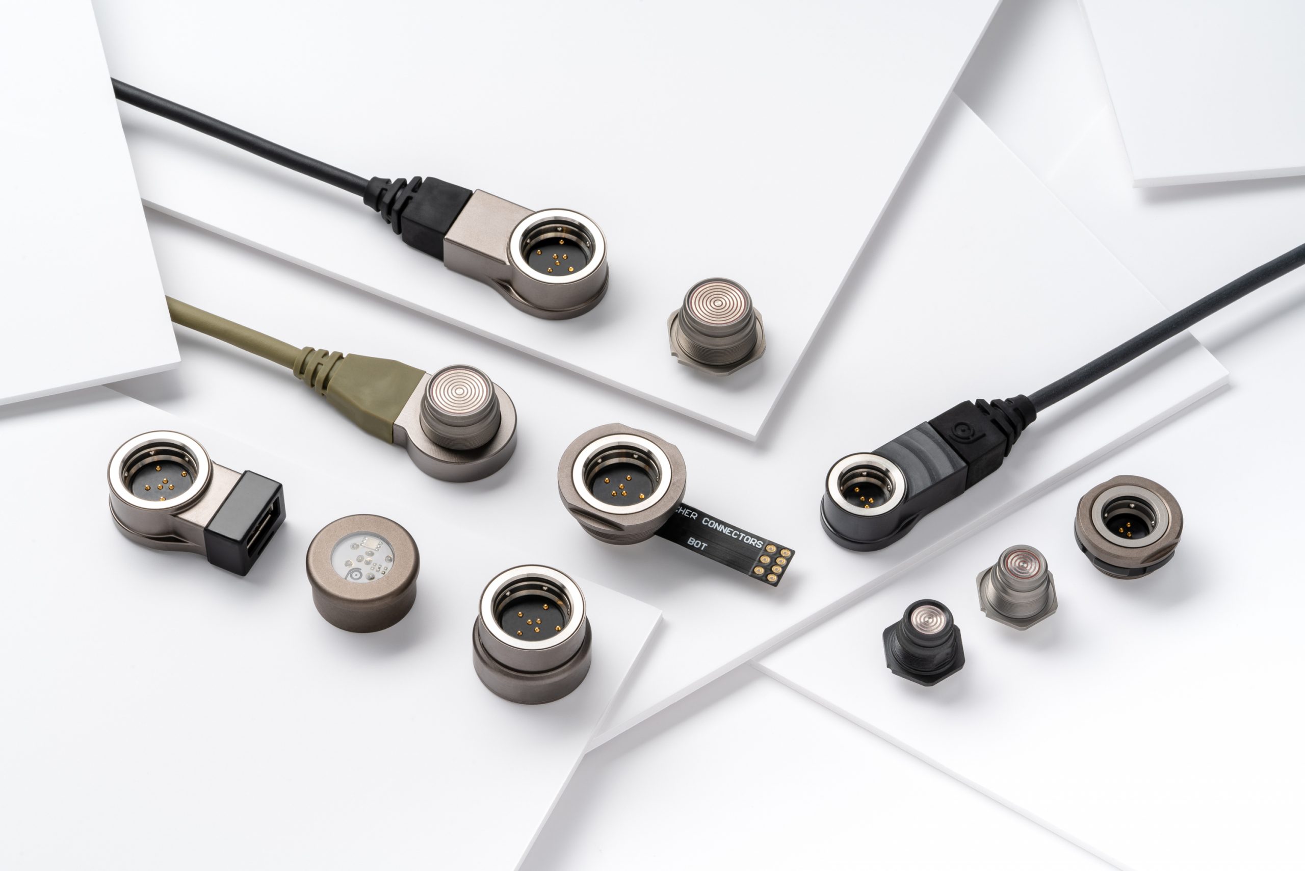
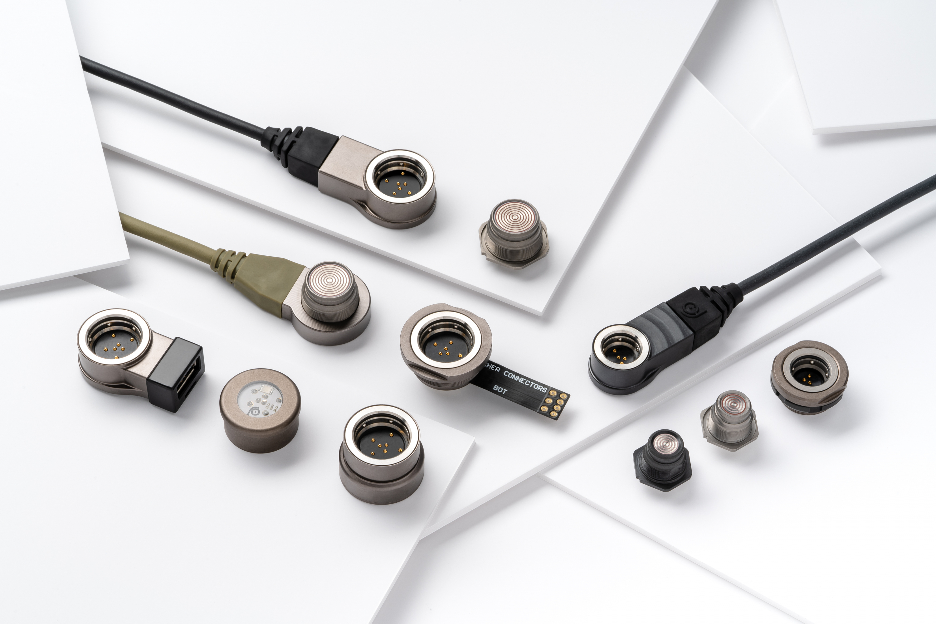
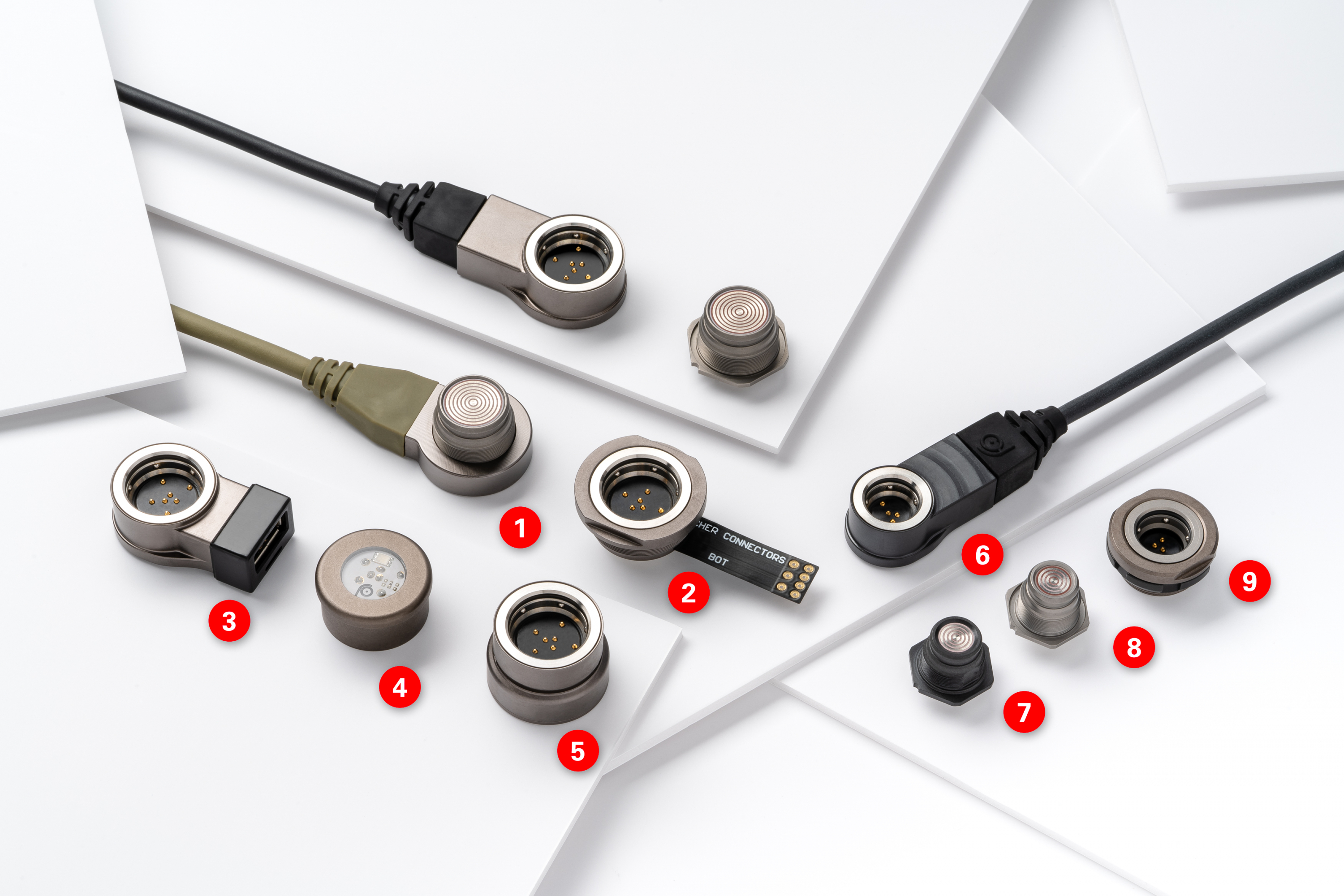
Nine new products now add to the capability of the Fischer FreedomTM Series to serve as a technology platform in connectivity setting new standards in usability, integration capability and versatility. An innovation enabler in application design, particularly in terms of SWaP (Size, Weight and Power) requirements, cable management optimization, electronic network integration and wearable technology.
The new features, new configurations, new materials and new active devices, commercially available as of September 2019, use the versatile and modular connectivity technology of the Fischer LP360TM connector, the first product of the plug & use Fischer FreedomTM Series launched in 2018 (cf. top of photo below):
No key code and non-magnetic quick-release locking for easy 360° mating
Membrane-sealed contacts for easy cleaning
Easy integration thanks to low-profile design and ergonomics
Fischer FreedomTM enables design engineers to integrate more technology and functionality into fixed or wearable ecosystems and cable-free devices in markets such as: defense & security, medical, instrumentation, industrial and civil engineering, robotics, wearables, the Internet of Things (IoT), etc.
The new USB 2.0 adaptor, LED and flash drive have the Fischer LP360TM panel plug directly integrated into their housing. This opens up new development pathways for innovative active solutions integrated into electronic networks where power source and communications are centralized within shared data & power buses and hubs. As for the new cabled receptacle in metal with 7 signal and power contacts, it is a ready-to-use solution that also maximizes the usability, operability and functionality of robotic systems or smart vests into which it can easily be integrated. These solutions are ideally used in applications for portable and body-worn “wearables”, among others, for the so-called “connected human” – a huge trend in the connectivity sector –, as well as in IoT applications.
NEW Fischer LP360TM products. Size 14 (7 signal & power contacts): cabled receptacle (1) and panel plug (2); active devices: USB 2.0 adaptor (3), LED (4), Rugged Flash Drive (5). Size 08 (4 signal & power contacts) in plastic (high-end composite based on PEEK) with cabled plug (6) and panel receptacle (7); in metal with panel receptacle (8) and panel plug (9).
Fischer Connectors Group’s CEO Jonathan Brossard says:
“Fischer FreedomTM is more than a traditional connector product line. It is a real technology platform which also enables innovations in active solutions with the goal, among others, to maximize the usability, interoperability and multifunctionality of electronic devices and ecosystems. I’m extremely proud that our Product Development and R&D teams have been able to launch such a variety of new products at the same time. They demonstrate our capacity to deliver reliable and versatile connectivity solutions that create innovation synergies in diverse markets.”
Fischer Connectors’ R&D Director Jérôme Dabonneville adds:
“Fischer FreedomTM is instrumental in making our customers’ lives easier. Its plug & use technology is not only an innovation enabler and accelerator in terms of connectivity and device development. It also allows what we call a ‘connectivity by design’ process. Connectivity design can (and should) take place upstream in the device design process, not downstream. With this new versatile and modular technology at hand, our customers – mainly design engineers and integrators – can now design their devices from the outset. The new product extensions widen the choice of solutions out of their engineering toolkit.”
Fischer FreedomTM was launched in June 2018 by Fischer Connectors, the global provider of ultra-reliable and high-performance connectivity solutions, to offer breakthrough plug & use technology. Thanks to the patent-pending technological innovations in mating, locking and materials, of its first product, the Fischer LP360TM 7-pin connector, the connectivity solution has received four awards in one year, and has been recognized as being able “to change the way connectivity is done”, as a LEAP award judge commented.
The new extensions of Fischer FreedomTM will be unveiled as a world premiere at the Defence & Security Equipment International (DSEI) tradeshow in London, UK (10-13 Sept.) and at the All About Automation tradeshow in Leipzig, Germany (11-12 Sept.).
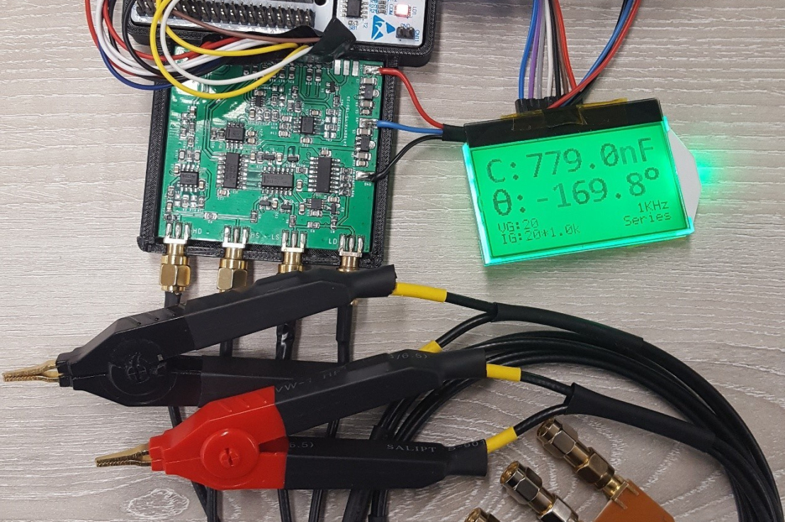
Adil Malik made a low cost FFT LCR meter with an STM32 MCU:
The approach I took was a mixed signal one where a capable analog front end would be paired up with a beefy DSP processor to compute the Impedance. Most importantly, in this scheme, the DSP is responsible for discriminating the phase between the sampled voltage and current waveforms; this approach is preferred because it leads to good accuracy and calibration stability.
Low cost high accuracy STM32 FFT LCR meter – [Link]
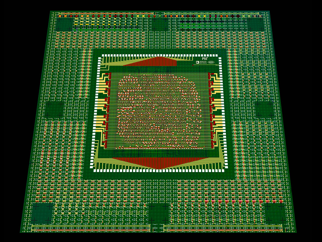
Did you know that researchers are looking for an alternative to silicon? Did you know in principle that Carbon Nanotubes processor could run three times faster while consuming about one-third of the energy of their silicon predecessor? The Engineers at MIT and Analog Devices have created the first fully programmable 16-bit Carbon Nanotube microprocessor.
Since Silicon Transistor is no longer shrinking as it used to and some of its inefficiencies are also becoming exposed with switches leaking current while circuit based on them gets hot. The problem is only becoming worse with transistors becoming smaller and circuits getting denser. However, as a solution, a team of researchers is hunting for an alternative to silicon with Carbon nanotubes which have long shown promise of being a viable alternative.
Carbon nanotubes are tubes made of carbon with diameters typically measured in nanometers. They are almost atomically thin and as a result of this, they conduct electricity very well and can be said to be better semiconductors than silicon. Leveraging on these features, carbon nanotubes can not only make traditional chips more powerful, but they can also be used to create entirely new computing systems— which are ultrafast and efficient three-dimensional chips that can be employed in data centers as well as the wide world of computing elements used in cars, smartphones, and the sensor-filled Internet of Things.
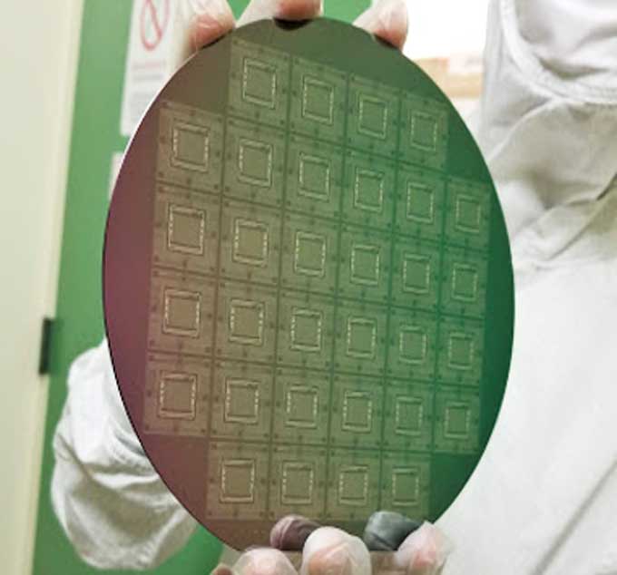
However, until now, they have proved too difficult to use in constructing a complex computing system but the team of researchers led by Professor Max Shulaker has successfully built a chip using them and the chip was tested by running a simple program “Hello World!”. The developed chip is the most complex integration of Carbon nanotube-based CMOS logic so far with nearly 15,000 transistors.
While the milestone is a great one, there are a few issues encountered by the researchers. One of the issues is the Carbon nanotube purity, with each batch of semiconducting carbon nanotube, containing 0.01 percent of metallic nanotube which is undesirable as they act as wires and they can short out the circuit, waste power and/or produce noisy signals. To solve this, Shulaker and colleagues came up with a solution to design a separate circuit with a good combination of logic gates and avoid using the bad combination that was most confused by the metallic nanotube glitches.
Another problem the team faced was the uniformity of the carbon nanotubes, the tubes tend to bunch together in lumps when a network of carbon nanotubes is deposited onto a computer chip wafer and this prevents the transistor from working. This problem was solved by Shulaker’s team by first coating the nanotube covered substance with photoresist and then carefully washing it under just the right conditions. The process selectively removes the bundles but leaves the individual Carbon nanotubes.
After overcoming all of this hurdles, the team was able to create two types of transistors that are needed for the CMOS logic, these transistors are the kinds which are in use in all kinds of processors for decades and this was a big breakthrough called MIXED.
Going forward, 3D systems could mix carbon nanotubes and emerging memory technologies, and they could also be built directly on top of conventional silicon circuitry. So while carbon nanotubes may eventually leap ahead of silicon, they could also share the road with it. In both cases, the resulting massive advances in computational capability would affect computing profoundly
Arbor Technology has announced a new inclusion to its ELIT series of digital signage systems equipped with Intel’s 8th Gen Coffee Lake S-series Core processors with 35W TDPs. The fan-less, rugged “ELIT-1930” signage player runs Linux or Windows on an 8th Gen Coffee Lake-S CPU with up to 32GB DDR4, and features triple 4K displays, 2x GbE, 3x COM, 4x USB 3.1, and 3x M.2. The ELIT-1930 offers Linux 4.x or Windows 10 IoT on CPUs including the 6x core/12x thread Core i7-8700T which is clocked at 2.4GHz/4GHz. Available also is a hexa-core i5-8500T, and quad-core i3-8100T, which are single-threaded, with the system having an Intel Q3. Another Coffee Lake based signage player we’ve seen with Linux support is Axiomtek’s similarly S-series based OPS700-520. A large number of Arbor’s ELIT signage players have been Intel-based systems, such as the 6th Gen Skylake based ELIT-1900.
Arbor also offers an Arm-based model: the ELIT-300 with an unidentified quad-core, Cortex-A17 SoC (probably the Rockchip RK3288). The ELIT-1930 is larger (210 x 190 x 70mm), and has a more feature-rich design than the ELIT-1900. It supports twice the RAM of the ELIT-1900, offering up to 32GB of 2400/2666MHz DDR4 via dual sockets. The announcement page mentions support for up to 4096 x 2304 at 60Hz video via the DP 1.2 and the HDMI ports. In contrast, the spec list shows 3840 x 2160 @ 60Hz for both. The ELIT-1930 offers a DVI-D port for up to 1920 x 1080 @ 60Hz, which enables triple simultaneous displays.
Key Features
Support triple-display for 1 x HDMI, 1 x DVI- D and 1 x DP
Support one channel 4K (UHD) Display
Support 3 x COM, 4 x USB3.1 with Type A
Support DirectX 12
Support iAMT Function
Support RAID Function
One NGFF connector for wireless
RTC wakeup supported
Operating temperature : -10 ~ 50°C
The ELIT-1930 is also equipped with 2x Intel-based GbE ports, one of the ports supports iAMT when using the Core-i7 and -i5 parts. Available also are 4x USB 3.1 ports (generation unspecified) and 3 x RS-232/485 ports (1x DB-9, 2x RJ-45). It is further equipped with a watchdog, an RTC, LEDs, and a PS/2 port. Expansion feature is enabled through 3x M.2 slots. The ELIT-1930 offers an M.2 E-Key 2230 socket (PCIe x1, USB 2.0) for a WiFi/Bluetooth card plus an M.2 M-Key 2280 (SATA, PCIe x4) and an M.2 B-Key 2242 (PCIe x1, USB 3.0), with the latter offering an optional BIOS switch to SATA and USB 3.0 with RAID support. It also offers optional antennas and WiFi/BT and LTE modules.
The ELIT-1930 offers a -10 to 50°C range, and offers vibration (3 Grms / 5~500Hz / random), shock (40G, 11ms), and humidity (10 ~ 95% @ 50°C, non-condensing) resistance. It also features a wall-mountable system that has a 12-24V DC input with optional 120W AC/DC 19V adapter kit and runs at a maximum of 60W without I/O card.
Further information
Pricing or availability information is not provided for the ELIT-1930 yet. More information can be found in Arbor Technology’s announcement and product page.
In the introduction tutorial Amplifier Classes, we have presented the different classes of amplification that can be found. In this article, we will focus more in detail about the Class A amplifiers.
Before going into the core of the topic by presenting different Class A configurations, it is important to have in mind the selection criteria of an amplifier class :
The ratio η=Pout/Pabs that highlights the efficiency of the amplifier.
The voltage and current gain.
The distortion which shows how faithfully the output signal is reproduced.
The maximal working frequency.
It is also important to keep in mind that the class of an amplifier is fully determined from the biasing parameters : the power supply Vsupply, and the resistances of the voltage divider network.
Class A overview
The aim of this section is to get a reminder of the general characteristics of a Class A amplifier before talking about new configurations.
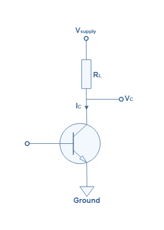
In the case of a Class A amplification, the biasing is chosen such as the operating point is located in the middle of the load line : VC0=Vsupply/2 and IC0=VC0/RC with RC being the resistance of the collector branch.
As seen during the Amplifier Classes tutorial, class A amplifiers have a 360° conduction angle, meaning that 100 % of the input signal is used for the amplification process. Their efficiency is very low with a theoretical maximum of 50 %. We will see in the next section, however, that this last affirmation is valid only for a certain architecture.
Class A configurations are generally low power amplifiers. Moreover, the output load is fixed, that means that they are optimally designed to be connected to a specific load value : either to another amplifier or to a specific loud speaker.
Due to these features, Class A amplifiers are mostly found in the most common type of BJT configuration : the Common Emitter Configuration (CEA). In the next sections, we present two different configurations of Class A amplifiers based on a CEA structure. Everything that we will mention applies to other configurations such as the Common Collector Configuration or the MOSFET.
Basic Common Emitter Configuration in Class A
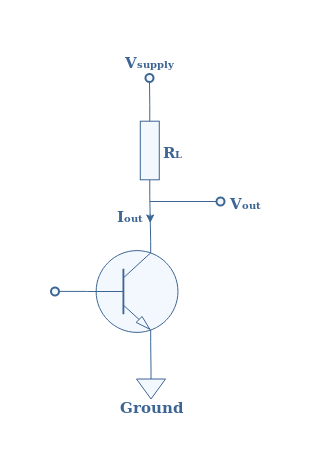
In this section, we present the basic configuration of a Class A amplifier using the CEA as an example. The output stage of the CEA is shown in Figure 1 below :
fig 1 : Output stage of a basic CEAA
This is the most basic configuration for a Class A power amplifier, note that the load resistance RL is directly wired to the collector branch. In the following, we will refer to this configuration as basic CEAA for Common Emitter Amplifier Class A.
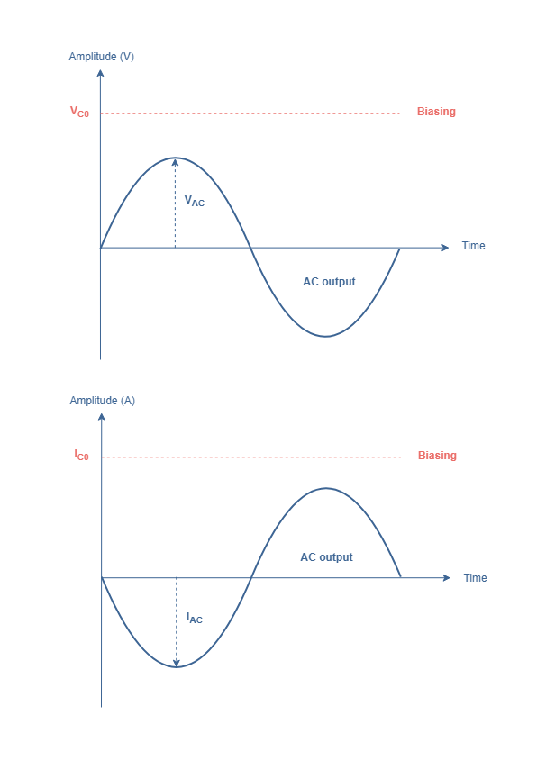
In Figure 2 is presented how the output signal can be decomposed into two components : the biasing DC signal and the AC amplified signal :
fig 2 : DC and AC component of the output signals
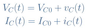
The very visual decomposition of the output signal shown in Figure 2 into one DC component (VC0,IC0) and one AC component (vC(t),iC(t)) allows us to write for the total output signals VC(t) and IC(t) :
eq 1 : Decomposition of the output signals
For a pure resistive load such as in Figure 1, vC(t)=VAC×sin(ωt) and iC(t)=-IAC×sin(ωt). The symbol ω represents the angular frequency : ω=2πf.
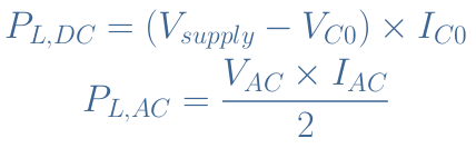
The instant power absorbed by the load PL(t) comes from the contribution of the biasing signal and the alternative signal : PL(t)=(Vsupply-VC(t))×IC(t). It can be shown through an integral calculus over one period of the signal that the average absorbed power PL can be decomposed into one power due to the biasing PL,DC and one useful power due to the signal variations across the load PL,AC :
eq 2 : Average DC and AC power absorbed by the load
The total power Ptot supplied to the amplifier comes from the DC power supply : Ptot=Vsupply×IC0. The efficiency of the configuration of Figure 1 is therefore the ratio of the useful power over the total supplied power : η=PL,AC/Ptot.
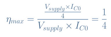
From the expression of PL,AC given in Equation 2, the efficiency is maximum when VAC and IAC are maximized, that is to say for VAC,max=Vsupply/2=VC0 (see why in Figure 3) and IAC,max=IC0.
The maximum efficiency is thus :
eq 3 : Maximum efficiency for a basic CEAA configuration
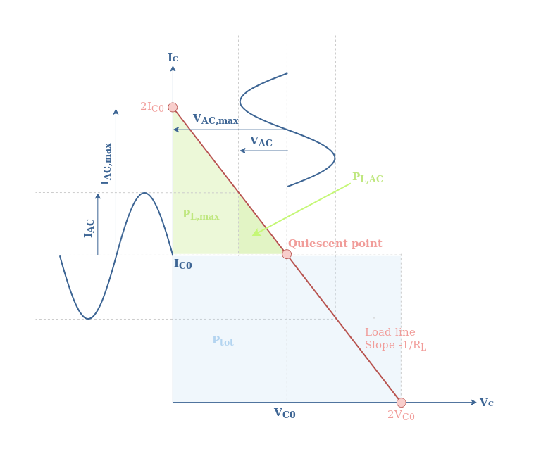
All of the information detailed above can be synthesized in the following Figure 3 :
fig 5 : Distribution of power for a basic CEAA
The light blue area represents the total power Ptot supplied to the system. It is very visual here to see that the useful power absorbed to realize the amplification process PL,AC (in light green) represents only a small fraction of Ptot. To overcome to this very low efficiency, one of the solution is coupling the collector branch with a transformer as we will see in the next section.
Transformer-coupled configuration
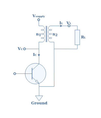
We present here another configuration of the CEAA that involves the use of a transformer. The following configuration will be referred to as transformer-coupled CEAA. The output stage of this architecture is presented in Figure 4 below :
fig 4 : Output stage of a transformer-coupled CEAA
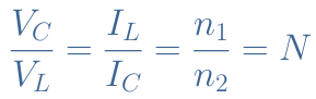
First of all, let’s give a short talk about what a transformer consists of. It is a passive component that transfers energy between two decoupled circuits. It works with generally two inductances wired around a core, the number of turns of the first inductance is n1 and n2 for the secondary circuit. The input (here VC,IC) and output signals (here VL,IL) of a transformer satisfies :
eq 4 : Ideal transformer identity
Thanks to the transformer, the load is decoupled from the collector branch, therefore the operating point of the amplifier changes. Indeed, no resistance is interposed between the power supply and the collector branch. Moreover, since the inductance do not block DC voltages, we can consider the DC resistance of the transformer to be equal to zero.
In a basic CEAA (see Figure 1), the biasing voltage is VC0=Vsupply/2. For the reasons we mentioned above, in a transformer-coupled CEAA, , the biasing voltage becomes VC0=Vsupply.
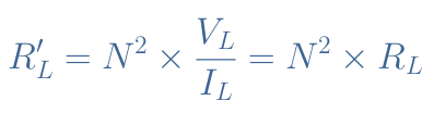
The slope of the load line will be given by -1/R’L where R’L is the apparent load in the primary circuit.
The expression of the apparent load is defined such as R’L=VC/IC. From Equation 4, we know that VC=N×VL and IC=IL/N. It comes therefore, that the apparent load is given by :
eq 5 : Apparent load in the primary circuit
As shown in Figure 2 for the basic CEAA, we can decompose for the transformer-coupled CEAA the output signals in a DC component (Vsupply,IC0) and an AC component (VAC,IAC).
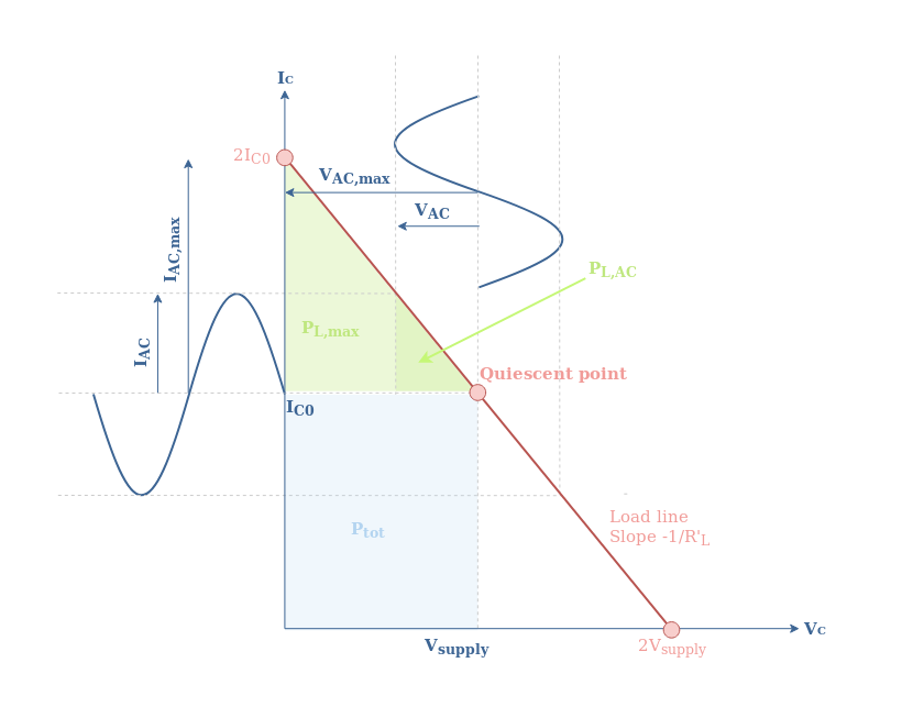
Having all of this information in mind, the diagram of power distribution of the transformer-coupled CEAA is presented in Figure 5 :
fig 5 : Distribution of power for a transformer-coupled CEAA
When comparing Figures 3 and5, we can clearly see that in the case of a transformer-coupled configuration, the proportion of the light green area representing the useful absorbed power for the amplification process is much larger.
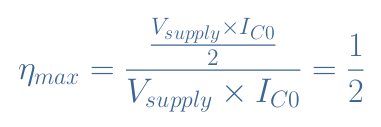
The efficiency is maximized when VAC and IAC are maximized. In this case, VAC,max=Vsupply and IAC,max=IC0. The maximum efficiency ηmax of a transformer-coupled CEAA is therefore given by :
eq 6 : Maximum efficiency for a transformer-coupled CEAA configuration
The efficiency of this configuration is improved by a factor of 2 when compared to the basic CEAA configuration. Ideal efficiency of 50 % can thus be achieved when coupling the output stage of a Class A amplifier with a transformer.
Conclusion
During this tutorial we have presented in details the characteristics and possible improvements of Class A amplifiers. As a reminder to the introductory article, we have seen that Class A amplifiers are biased such as 100 % of the input signal can be used for the amplification process. Moreover, they present a rather low efficiency, but a faithful reproduction of the signal.
The core of the tutorial deals with two configurations based on a Common Emitter Amplifier structure (CEA). The first one is the most basic architecture called “basic CEAA” with the load wired between the power supply and the collector branch of the bipolar transistor. The big inconvenient of the basic CEAA is that the operating (or quiescent) point is located in (VC0,IC0), which limits as seen in Figure 3 the useful power absorbed for the amplification of the AC signal. The efficiency of a basic CEAA is therefore limited to a theoretical maximum of 25 %.
The second architecture called “transformer-coupled CEAA” overcomes this problem by decoupling the load and the collector branch with the use of a transformer. The operating point is shifted to (Vsupply,IC0), allowing to increase the useful absorbed power with keeping the total supplied power unchanged as highlighted in Figure 5. The efficiency of a transformer-coupled CEAA is enhanced by a factor 2 reaching a theoretical maximum of 50 %.
Despite the improvement of efficiency brought by the transformer, it also brings some inconvenient. Indeed, the transformer induces an extra cost and an extra weight to the final product. The size of a transformer can also be restrictive for packaging purposes. Finally, extra complexity and cost need to be taken into consideration to protect the transistors against possible damages caused by back electromotive forces from the inductance.
In the next article of this series of amplifier classes, we will present in detail the Class B amplification that can overcome the low efficiency of Class A amplifiers.
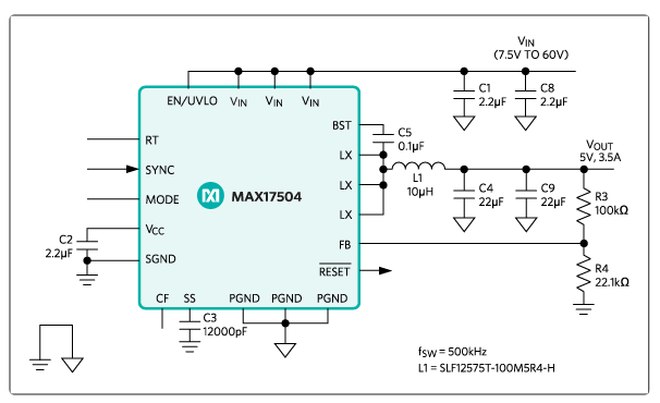
The MAXREFDES1048 synchronous step-down dc-dc converter reference design from Maxim Integrated Products is based on the MAX17504, a high-efficiency, high-voltage, synchronously rectified step-down converter with dual integrated MOSFETs can operate over a 4.5V to 60V input. The MAXREFDES1048 reference design operates over an input voltage range of 18- to 36-Vdc and delivers an output of 3A.
The MAX17504 can deliver up to 3.5A and generates output voltage from 0.9V to 90% VIN. Built-in compensation across the output voltage range eliminates the need for external components. The feedback (FB) regulation is accurate to within ±1.1% over -40°C to +125°C. The devices are available in a compact (5mm x 5mm) TQFN lead (Pb)- free package with an exposed pad. Simulation models are available.
The MAX17504 features a peak-current-mode control architecture with a MODE feature that can be used to operate the device in pulse-width modulation (PWM), pulse-frequency modulation (PFM), or discontinuous mode (DCM) control schemes.
MAXREFDES1048 evaluation board
PWM operation provides constant frequency operation at all loads and is useful in applications sensitive to switching frequency. PFM operation disables negative inductor current and skips pulses at light loads for high efficiency, allowing the DCM to feature constant frequency operation down to lighter loads than PFM mode.
A programmable soft-start feature allows users to reduce input inrush current. The device also incorporates an output enable/ undervoltage lockout pin (EN/UVLO) that allows the user to turn on the part at the desired input voltage level. An open-drain RESET pin provides a delayed power-good signal to the system upon achieving successful regulation of the output voltage.
Key benefits and features of the MAX17504 include the following:
Eliminates external components and reduces total cost
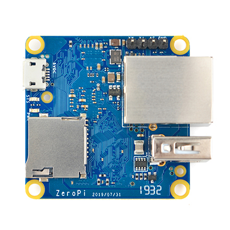
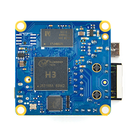
FriendlyELEC has recently launched a new family of boards called the “ZeroPi”. While they go by a name similar to that of the Arduino Zero Compatible development kit for robotic motion structure systems, the FriendlyElec ZeroPi boards are tons different as they feature an Allwinner H3 processor, a Gigabit Ethernet and are very similar to the fairly popular NanoPi NEO boards but they do not come with any I/O headers asides from breakout pins for serial communication.
The Zero Pi
The board was designed for users who would be connecting most of their peripherals over USB which explains why it does not come with headers. The board comes with a Micro SD card slot through which the operating system is booted but it also comes with the option to boot from the network (without the need of a microSD card) via the SPI flash.
Some of the ZeroPi specifications are highlighted below:
CPU: Allwinner H3, Quad-core Cortex-A7 Up to 1.2GHz
DDR3 RAM: 256MB/512MB
Connectivity: 10/100/1000Mbps Ethernet
USB Host: Type-A x 1
MicroSD Slot x 1
MicroUSB: for power input only
Debug Serial Port: 4Pin, 2.54 mm pitch pin header
Power Supply: DC 5V/2A
PCB Dimension: 40 x 40 x 1.2mm
Working Temperature: -20℃ to 70℃
Weight: 15g
OS/Software: u-boot, UbuntuCore
The ZeroPi runs the FriendlyElec’s FriendlyCore distro which users will need to download and flash there SD Card with. Since the FriendlyCore is based on the same distro like Debian, Ubuntu, OpenWrt, and DietPi, it comfortably supports any of them and they can all be used as the operating system for the ZeroPi. The compatibility with friendly core also brings support for the features listed below to the ZeroPi:
Support LCDs with both capacitive touch and resistive touch
Support WiFi (USB WiFi)
Support Ethernet
Supports Bluetooth
Supports audio playing (HDMI Audio)
Supports USB cameras and other USB Peripherals
Supports Qt 5.10.0 EGLES and OpenGL ES1.1/2.0
The 512Mb RAM version of the board is currently on sale for $12.99 on FriendlyELEC store with a metal or acrylic enclosure add-on for a few extra dollars. More information on the boards can be found on the product page or the ZeroPi wiki page.
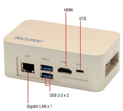
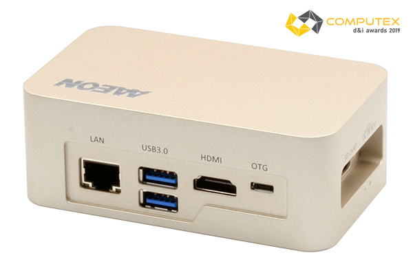
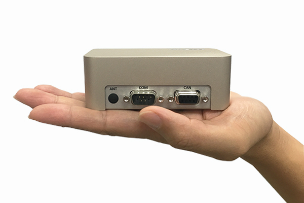
Aaeon has announced the release of the Boxer-8110AI embedded computer. The Compact board which is similar to Aaeon’s Boxer-8120A which was released in May is based on the Nvidia Jetson Tx2 Module and is capable of running Linux distros like Ubuntu.
While it offers a more compact size (110 x 65 x 40mm), just like the Boxer-8120A, the Boxer-8110AI it comes with 8GB of LPDDR4 RAM, 32GB eMMC 5.1, and a MicroSD slot. The board also comes with communication support like the Gigabit Ethernet, HDMI, CAN and Serial Communication.
Designed for industrial applications, to meet the physical requirement of industrial environments, the board comes with anti-vibration features (3 Grms/ 5 ~ 500Hz/ operation – eMMC), supports /tolerate extreme temperature levels between the range of -20 to 50°C with 0.5 m/s AirFlow according to IEC60068-2 for Industrial Device, withstand humidity values up to 95% @ 40°C non-condensing, and comes with CE and FCC Class A certification ensuring it won’t be a source of disruption to other systems.
Some of the critical features of the embedded computer are highlighted below:
Based on NVIDIA Jetson TX2
HMP Dual Denver 2 + Quad ARM A57 CPU
Support Linux Ubuntu 16.04
8GB LPDDR4, 32GB eMMC 5.1
HMP Dual Denver 2 + Quad ARM A57
HDMI 2.0 x 1, USB3.0 x 2
RS-232 x 1, CANBUS x 2 Channel
OTG x 1
LAN x 1
MicroSD x 1
The Nvidia’s Jetson TX2, which the Boxer-8110AI is based, is equipped with an Arm-based Tegra-family SoC with dual Cortex-A72-like “Denver” cores and 4x -A57 cores. The SoC incorporates 256-core Pascal graphics, supported with CUDA libraries for AI, vision processing, GPU-accelerated parallel processing, and deep/machine learning. Its integration on the Boxer-8110AI means it will be bringing all of these features and capabilities to the embedded computer.
Aside from the different range of AI frameworks including Tensorflow, Caffe2, and Mxnet, which are compatible with the Nvidia Jetson, users can also install their own AI inference software on the device making the BOXER-8110AI the perfect embedded computer for industrial edge AI applications.
The BOXER-8110AI’s CANbus and rugged design features (anti-dust measures, aluminum chassis, wide operating temperature range) means it can support industrial automation and in-vehicle applications. With its powerful processor and cost-effective design, this is one AI platform you’ll be able to install anywhere.
The Boxer-8110AI has a 12V DC input via a terminal block through which it is powered and it ships with a wall-mount kit used for mounting it to the wall.
The embedded computer is currently available for $1,033 ($34 cheaper than the Boxer-8120A) on Aaeon’s product and shopping pages.