The smart Inertial Measurement Unit (IMU) BMI270 scores with increased system battery life and an improved accelerometer. Optimised for wearable and hearable applications, the BMI270 is available from Rutronik UK.
The newest member of the BMI260 family of IMUs includes intuitive gesture, context and activity recognition with an integrated plug-and-play step counter. The IMU handles these functions independently of the main system processor, thus significantly extends system battery life. The powerful and accurate gesture and activity-recognition features therefore run in the ultra-low power domain, with current consumption of just 30µA.
This reduces power consumption and enables extended battery charging intervals. The BMI270 measures only 2.5 x 3.0 x 0.8 mm3, and is pin-to-pin compatible with the BMI160 and BMI260. The IMU is well suited for many types of wearable devices, such as smart clothes, smart shoes, smart glasses, wrist and ankle bands as well as hearables. Enabled by the new Bosch MEMS process technology, the BMI270 features a strongly improved accelerometer performance.
It saves OEMs valuable time and costs during testing and manufacturing. The BMI270 is available in two application-specific versions, A and C: The A version detects wrist gestures (flick in/out, pivot up/push, arm up/down, and jiggle) for intuitive control of e.g. smart watches and is designed for Wear OS by GoogleTM. The C version has advanced features for recognizing context / activity change (standing, walking or being in a vehicle).
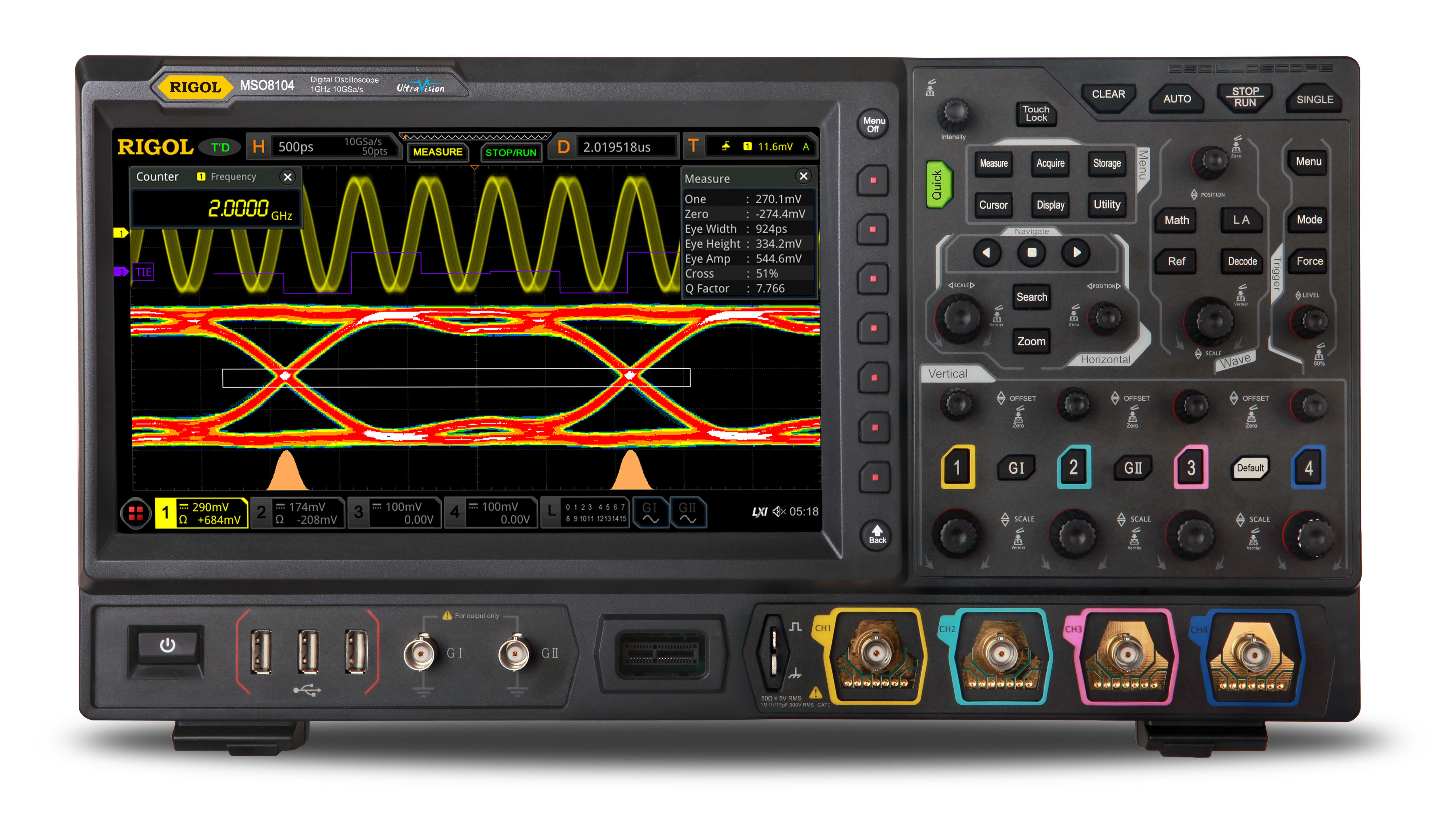
10GSa/sec sampling and 500Mpts memory depth makes these 600MHz/1GHz/2GHz 4 channel oscilloscopes stand out from the crowd.
Saelig Company, Inc. has introduced the new Rigol TechnologiesMSO8000 Series of digital oscilloscopes, which combine best in class sampling (10GSa/sec) and memory depth (500Mpts) with a modern, flexible user interface enabled by Rigol’s new UltraVision II architecture and innovative Phoenix chipset. Three models are available with input bandwidths from 600 MHz to 2GHz, each with 4 analog channels. The series is MSO ready: an optional 16-channel logic analyzer interface is provided to provide digital debug capabilities with the addition of 16 channel probes and software.
The advanced MSO8000 Series features a 10.1” 1024 x 600 capacitive multi-touch color LCD screen with 256-level intensity grading and a waveform refresh rate of up to 600,000wfm/sec. The enhanced FFT capability offers real-time spectrum analysis of up to 1Mpts of waveform data. The MSO8000 Series user interface provides five distinct ways to interact with the instrument: LCD Touch, traditional button and knob, mouse/monitor, PC control, and remote web operation. A two-channel 25MHz arbitrary waveform generator is also available.
The MSO8000 series utilizes Rigol’s proprietary Phoenix chipset, which allows sampling at a remarkable 10GSa/s, and integrates all of the front-end analog processing. All three models in the scope series provide non-stop recording and playback for a maximum of 450,000 frames of real-time waveforms using a segmented storage technique. Trigger conditions can be set to make a selective choice in capturing and saving the signals of interest.
With a total of seven unique integrated instruments (digital oscilloscope, 16-channel logic analyzer, spectrum analyzer, optional arbitrary waveform generator, digital voltmeter, 6-digit frequency counter and totalizer, and optional protocol analyzer, the MSO8000 Series allows customers to quickly identify and resolve complex design and debug challenges. The optional Protocol Analyzer supports RS232/UART, I2C, SPI, CAN, LIN, I2S, FlexRay, and MIL-STD-1553 serial bus. The protocol trigger and decoding operate on both the analog and the digital channels: RS232/UART, I2C, and SPI protocols. The Jitter firmware option supports real-time eye diagram and jitter analysis.
The MSO8000 series is field-upgradeable to higher bandwidths and is equipped with hardware pass/fail test function in the standard configuration, which can be useful for long length signal monitoring during design, and production test. Setting the test mask on a known “standard” waveform allows an automatic comparison with the signal under test to show a successful or failed test.
The MSO8000 series external interfaces include USB HOST&DEVICE, LAN(LXI), HDMI, TRIG OUT, and USB-GPIB (option). The series brings innovative analysis and visualization capabilities to embedded design, power analysis, serial decode, and RF applications. Made by Rigol Technologies Inc., a leading manufacturer of precision electronic instrumentation for test and measurement, the MSO8000 Series digital oscilloscopes are available now from Saelig Company, Inc., their USA technical distributor.
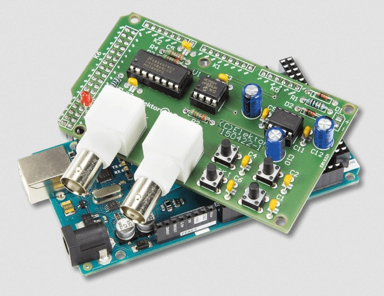
Original publication: Elektor magazine November 2016 Author: Kurt Schuster Free download expires: Friday 23 August, 2019.
Suppose you want to measure a slowly-varying voltage from a sensor, or perhaps plot the discharge curve of a battery. Is it really necessary to sit there and note down a reading from the multimeter every so many seconds or minutes? It is less tedious and much more elegant to use this Arduino-based unit connected to your oscilloscope. Two questions motivated Kurt Schuster at the beginning of this project: ‘is my battery any good?’ and ‘is this charger charging my battery correctly?’
Go to the article page and download a pdf copy of the magazine article. Downloading is free until Friday 23 August, 2019.
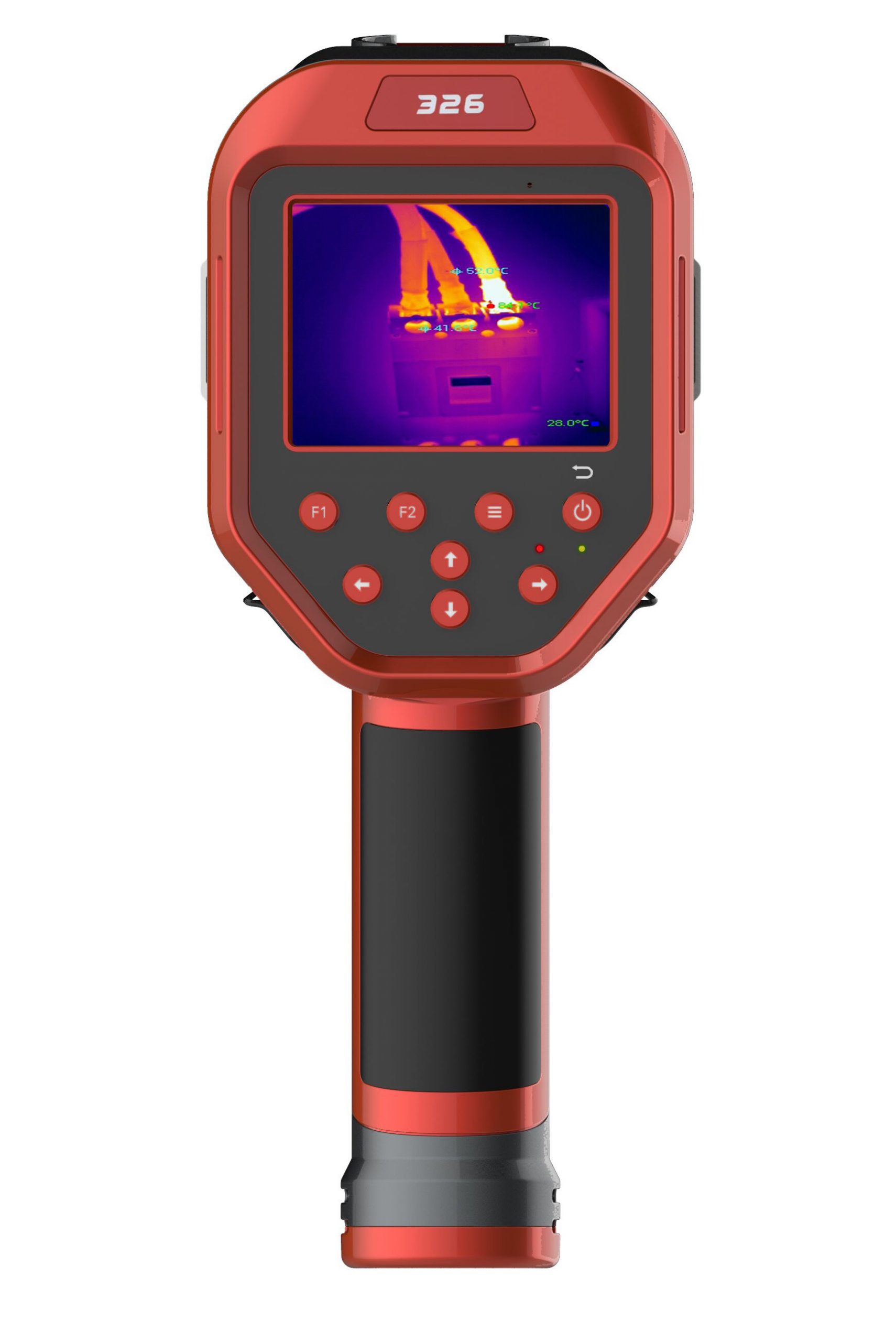
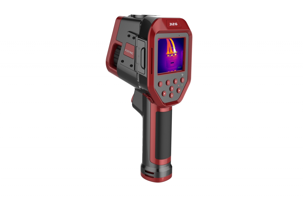
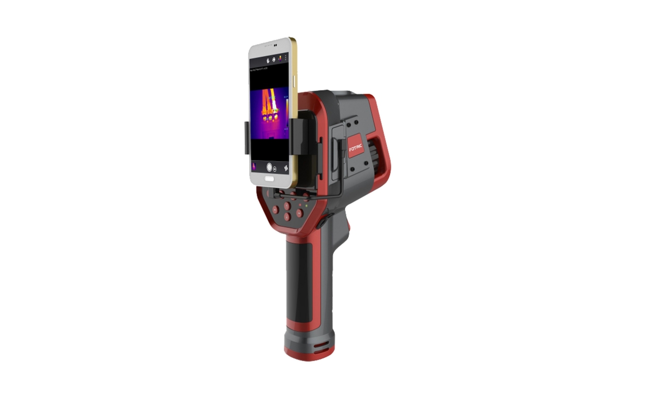
The Fotric 326 provides high quality radiometric images full of detailed thermal information in a handheld pistol-grip camera for investigative analysis
Saelig Company, Inc. (www.saelig.com) has introduced the FOTRIC 326 Thermal Imaging Camera – a rugged, durable, accurate, and portable handheld heat investigation device, designed for a wide range of equipment and infrastructure thermal diagnostic tasks. The 326 has a large aperture f1.0 IR lens for taking superior quality radiometric thermal images for professional use. The Fotric 326 has a –20degC to +650degC (-4degF to 1,202degF) measurement range to cover a wide variety of applications, especially when inspecting high-temperature objects. It offers an accuracy rating of ±2degC or ±2%, and a thermal sensitivity of 0.06degC (60mK). The Fotric 326’s thermal imager has a resolution of 384×288 to provide high quality, large radiometric images full of detailed thermal information. The adjustable focus lens facilitates precision imaging for objects of interest. The Fotric 326’s frame rate is 30Hz, faster than the 9Hz of many other thermal cameras. This gives smoother thermal images of rapidly changing thermal targets.
The 326 can produce a visible light image in addition to the thermal image, and allows picture-on-picture fusion of the two images to enable accurate problem location. User-defined temperature thresholds, audible and visual alarms of above/below temperature threshold, and adjustable focus make this a valuable thermal tool in an engineer’s arsenal.
The Fotric 326 has a useful built-in laser pointer to show exactly where the camera is pointed. Voice recording allows notes about the image to be saved audibly rather than handwritten. The audio message is saved with the thermal image and can be retrieved during post-processing.
The Fotric 326 has 3.5” screen display and it also supports mounting a smartphone as both the display and data processing center. The built-in flashlight is helpful when inspecting in low-light environments. The 326 can connect to the internet when using an Android smartphone as the display screen and data processing center. It then benefits from the powerful and advanced processing capability of the smartphone. With the Fotric LinkIR application installed on an Android smartphone, the 326 becomes an upgraded thermal camera with a full touchscreen HD user interface. The app provides capabilities such as taking radiometric video and sharing the thermal images instantly with others. With a smartphone installed as the display screen, the Fotric 326 can record short radiometric videos of up to 1,000 frames and up to 5 frames per second. Fotric 326 is provided with a 16GB memory SD card for storing at least 1,000 images, but larger SD cards can also be installed.
With good thermal resolution, together with high accuracy and sensitivity, the 326 is suitable for mechanical, electrical inspection, moisture detection, and building investigations. Applications include: leak detection, electrical problems, insulation issues, HVAC and air flow problems, mold and rot, pest infestations, equipment failures, tunnel inspections, etc.
Made by Fotric Precision Instruments, an innovative intelligent thermal imaging products manufacturer, the Fotric 326 camera is available now from Saelig Company, Inc., Fotric’s authorized North American distributor starting from 2.807 USD.
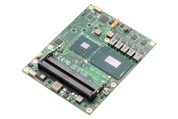
AAEON, an industry leader in embedded computing, announces the COM-CFHB6 Computer-on-Module. Featuring the 8th and 9th Generation Intel Core Processors, it is built to bring flexible computing to any embedded project.
The COM-CFHB6 is built to the COM Express Type 6 form factor. It features a wide range of processors from the Intel Celeron to Intel Xeon, and the 8th and 9th Generation Intel Core processors (Coffee Lake H/Coffee Lake Refresh). The COM-CFHB6 supports low power 25W processors, perfect for mobile applications, up to 45W 6-core Xeon server CPUs. Combined with support for up to 48 GB DDR4 memory with ECC support (Xeon, Core), the COM-CFHB6 is built to provide high performance in the most demanding of applications.
The COM-CFHB6 is built for flexibility with powerful I/O and expansion features. It supports four USB 3.1 Gen 2 ports and eight USB 2.0 ports, up to three display ports, and up to 24 PCI Express 3.0 lanes, perfect for edge computing and AI applications. The COM-CFHB6 also features a slim cooler design, only 28 mm tall, allowing the COM-CFHB6 to fit into almost any tight space.
With the combination of power and flexibility, the COM-CFHB6 is right at home with a wide range of applications, including digital signage, factory automation, and robotic controller. It can even be used as an edge device or AIOT gateway in Smart City applications.
AAEON also offers Q-Service Plus for the COM-CFHB6, our manufacturer and OEM/ODM service. AAEON works closely through the entire process, from board design, BIOS setup, and product testing, to provide an embedded solution that is built for your specific needs.
“Whether your application is in transportation or medical devices, the COM-CFHB6 is a powerful solution that can bring edge computing to your project,” said David Huang, Product Manager of Embedded Computing at AAEON. “With the COM-CFHB6, your project will have the power it needs to get the job done.”
SEGGER Embedded Studio V4.20 adds fully configurable support for debug probes using the GDB protocol. The new version can now be used with any debug probe that comes with a GDB Server.
This new feature is included in all editions: ARM, Cortex-M, and RISC-V, on Windows, macOS, and Linux 32- and 64-bit platforms.
Embedded Studio can automatically launch the 3rd party GDB Server upon starting a debug session, keeping debugging easy and convenient. Port number, host and protocol features are configurable for maximum flexibility. The GDB Server software is executed in a separate process and thus does not affect the stability of Embedded Studio.
The new implementation is tested and ready-to-go with J-Link GDB Server, OpenOCD, as well as ST-LINK GDB Server on Windows.
Embedded Studio can be easily downloaded from www.segger.com and fully evaluated without code size, feature or time limit. It can be used free of charge for educational and non-commercial purposes, without requirement to register.
“SEGGER has a broad spectrum of products. For many customers, this means we are a One-Stop solution for their needs,” said Ivo Geilenbrügge, Managing Director at SEGGER. “All products follow the same design rules and work seamlessly together. SEGGER has a long history of cooperating with other suppliers in the embedded space. If our customers, for whatever reason, prefer to combine a 3rd party or Open Source Product with our solutions, they can. This new release enables users of debug probes other than our market-leading J-Link to take full advantage of Embedded Studio.”
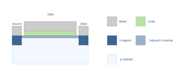
We have already seen in detail that a signal amplifier can be made with a Bipolar Junction Transistor (BJT). There are however other types of transistors that can be used to build an amplifier architecture and in this tutorial, we will focus on one of them : the MOSFET (Metal Oxide Semiconductor Field Effect Transistor). In a BJT, the Base act as the command signal to control the current flow between the Emitter and the Collector. In a MOSFET the command branch is named the Gate and it controls the current flow between the Source and the Drain.
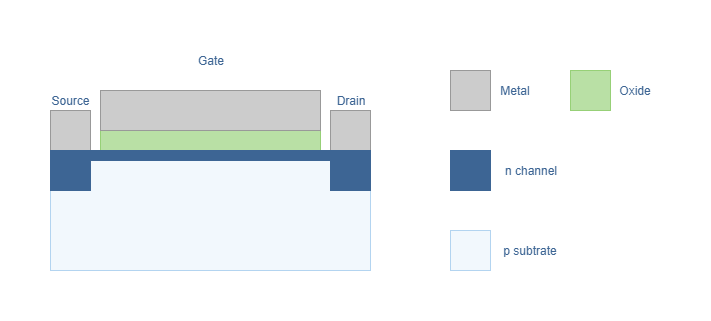
In the first figure below, the structure of a MOSFET is presented :
fig 1 : Depletion NMOS structure
First of all, let’s define the meaning of “depletion” and NMOS terms. The term “depletion” here refers to the fact that a physical channel is linking the drain branch to the source branch. This means that a current can pass through the MOSFET with no voltage applied to the gate. The current can be blocked by applying a negative voltage to the gate, that by field effect, will push electrons and attract holes. The term “NMOS” refers to the fact that the channel is built based on a N-doped region of silicon (excess of electrons) on top of a P-doped substrate (excess of holes). The current traveling in the MOSFET is therefore positive. P-doped channel transistors on top of N-doped substrates are called PMOS and the current through this type of MOSFET is negative.
One interesting aspect of the MOSFET is the silicon oxide layer that provides a total insulation between the gate and the channel, hence, the current in the gate is considered to be zero. In reality, there is a small leakage current of a few pA (10-12 A). In Figure 2 we present the structure that will be considered for the rest of this tutorial :
fig 2 : Enhanced NMOS structure
In this NMOS structure, there is no physical built-in n-channel between the drain and the source branches. This different structure is referred with the mention “enhanced”. The channel is electrically induced by applying a positive voltage to the gate that by field effect, attracts electrons and pushes the holes of the interface p-substrate/oxide.
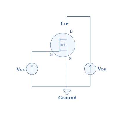
Electric diagram
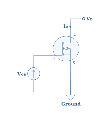
In Figure 3 below, we present a simple electrical diagram of a MOSFET. We define in this diagram the drain current ID, the drain voltage VD, the gate-source voltage VGS and the location of the gate, drain and source mentioned by the letters “G”, “D” and “S”.
fig 3 : MOSFET electric diagram
The gate and drain voltages VGS and VDS are mentioned with the subscript “S” because the source is grounded. Note that usually, the gate is a voltage source while the drain voltage is just measured and not imposed.
Electric behavior
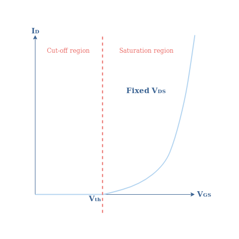
Characteristic ID=f(VGS)
In this section, we will describe how the drain current behaves when :
The drain voltage is imposed and the gate voltage varies : ID=f(VGS)
The gate voltage is imposed and the drain voltage varies : ID=f(VDS)
Let’s first of all focus on the characteristic ID=f(VGS) as presented in Figure 4 :
fig 4 : Characteristic ID=f(VGS)
It is interesting to note that the creation of the conducting channel is not triggered instantly by a positive voltage since no drain current is observed when VGS<Vth where Vth stands for “threshold voltage”. This first region is called the “Cutoff” or “Subthreshold” region. In this mode, the MOSFET acts as an open switch, allowing no output current to be induced.
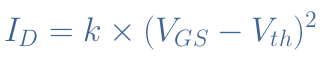
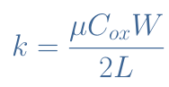
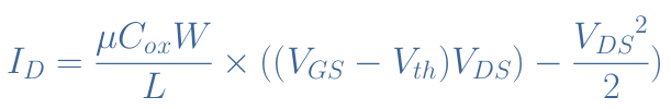
When the gate voltage is above the threshold value VGS>Vth, the drain current rises drastically. This second region is named “Saturation region” and we explain why further in the tutorial. In the saturation or “active” region, the current drain satisfies a parabola relation :
eq 1 : Expression of the current drain in the saturation region
The factor k, known as conduction factor, depends only on physical parameters of the MOSFET : the ratio Width (W)/Length (L) of the conducting channel between the drain and the source, on the electron mobility μ and the value of the capacitance formed by the metal-oxide-semiconductor structure of the gate Cox :
eq 2 : Expression of the conduction factor
It is interesting to analyze quickly this formula to understand the physics behind the MOSFET. The position on the numerator of μ, Cox and W indicates that if their value increases, the conduction factor and thus the current increases. Indeed, when W increases, the path for electrons gets wider and therefore the current increases. If the electron mobility increases, the electrons move faster, which in turns increases the drain current. If the capacitance increases, it will increase the drain current due to a higher concentration of electrons at the interface semiconductor/oxide. Finally, if the length of the conductive channel increases, the current will decrease since it faces a longer path, therefore a higher resistance.
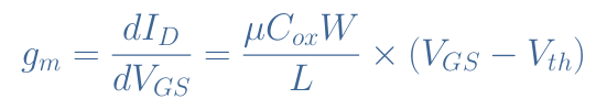
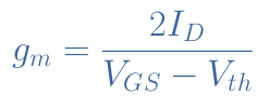
An important parameter can be derived from Equation 1 and Equation 2 which is called the transconductance (gm) of the MOSFET and is expressed in Amps / Volts or Siemens (S). :
eq 3 : Definition of the transconductance
Equation 3 can be rearranged by expressing the difference (VGS-Vth) as a square root from Equation 1 and after a few steps we get :
eq 4 : Expression of the transconductance
For a given MOSFET, that is to say, a fixed conduction gain, the transconductance only depends on the command voltage VGS and the current drain ID that are given by the characteristic ID=f(VGS) in Figure 4. The transconductance gives the gain of a MOSFET configuration but also the bandwidth, the noise performance and its linearity.
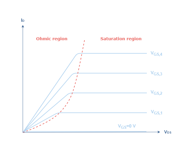
Characteristic ID=f(VDS)
To plot the second characteristic, we consider a set of gate voltages satisfying VGS,1<VGS,2<VGS,3<VGS,4. The characteristic ID=f(VDS) is constructed partially from the first characteristic ID=f(VGS). Indeed, the red dashed boundary in Figure 5 is given from the shape of the curve in Figure 4 :
fig 5 : Characteristic ID=f(VDS)
We can understand from Figure 5 why the saturation region first mentioned in Figure 4 is called such as. Indeed, in this region the drain current ID remains constant for a fixed bias voltage VGS no matter the value of the drain voltage VDS. This affirmation can be verified with the Equation 1 where VDS does not appear in the formula of ID. Therefore, the NMOS operates as a closed switch in the saturation region.
Before the saturation effect occurs, the MOSFET behaves differently in a region called “Ohmic”, “Triode” or “Linear” region. In this region, the expression of ID is quasi-linear affected by a decreasing parabola when VDS increases :
eq 5 : Expression of the current drain in the ohmic region
The boundary between the linear and saturation regions is given by the pinch-off voltage VP=VGS-Vth.
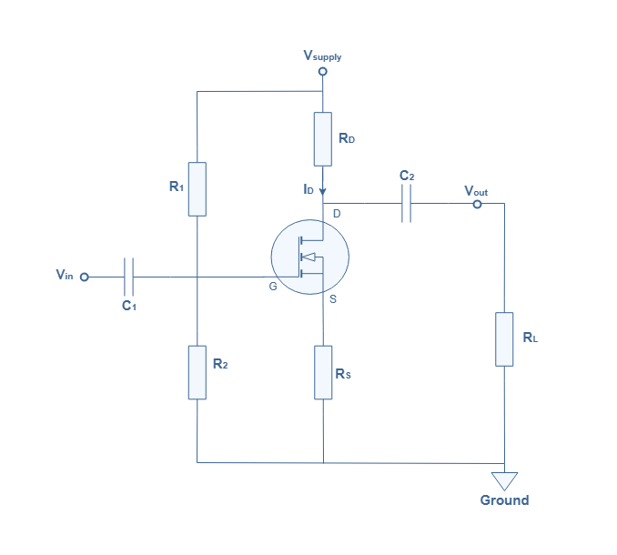
A MOSFET amplifier
A real and full MOSFET amplifier architecture is done by adding to the circuit of Figure 3 a biasing circuit, a drain, source and load resistor and coupling capacities :
fig 5 : Full MOSFET configuration
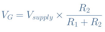
The biasing circuit consists of a voltage network divider, its role and functioning has been already dealt many times in the BJT amplifiers tutorial series, it is realized with two parallel resistor R1 and R2. The coupling capacitors C1 and C2 insulate the biasing DC voltage from the AC signal to be amplified. Finally, the output is delivered to a load, modeled by the resistance RL. The gate or bias voltage is given by :
eq 5 : Expression of the gate voltage
The values of R1 and R2 are generally large in order to increase the input impedance of the amplifier and to decrease the ohmic power losses.
Input and output voltages
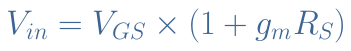
To simplify, we will consider that no load is placed in parallel with the drain branch. The input voltage is given by the gate to source voltage VGS and the voltage drop across the resistance RS given by RS×ID. Since by definition of the transconductance, ID=gm×VGS, the input voltage Vin can be factored by VGS such as :
eq 6 : Expression of the input voltage
The output voltage is simply given by the voltage drop across the drain resistance :
eq 7 : Expression of the output voltage
Voltage gain
The voltage gain AV is given from the ratio of Equation 7 and Equation 6, after simplifications it becomes :
eq 8 : Expression of the voltage gain
The sign “-” comes from the fact that in analogy with the BJT Common Emitter Amplifier, the MOSFET amplifier inverts the output signal : the phase is shifted of 180 ° or π rad.
Conclusion
This tutorial focused on Metal Oxide Semiconductor Field Effect Transistors (MOSFET) amplifiers. The MOSFET is an active component that consists of a conductive channel encapsulated between a semiconductor substrate and a metal/oxide structure. We have specially described enhanced NMOS structures that allow a current to pass when the command or gate voltage is positive and above a certain threshold value. We have seen that in order to understand the electric behavior of this transistor, two characteristics need to be analyzed. The first one, ID=f(VGS) gives the important parameter known as transconductancegm which helps to determine MOSFET’s amplifier gain that we give in the last section of the tutorial. It also gives the shape of the boundary between the linear and saturation regions of the transistor that can be represented in the second characteristic ID=f(VDS). From this analysis, three regions have been highlighted :
The cutoff or sub-threshold region where VGS<Vth and no current drain circulates in the channel.
The ohmic, linear or triode region where VGS>Vth and VDS<VGS-Vth and the drain current behaves linearly with the drain voltage.
The saturation or active region where VGS>Vth and VDS>VGS-Vthand the drain current remains constant for a fixed gate voltage despite of drain voltage variations.
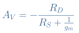
Finally, we have seen how a full MOSFET configuration can be achieved with a bias circuit and described the input and output voltages of the circuit and it’s voltage gain. The MOSFET amplifier inverts the voltage signal and provides a maximal absolute gain given by the ratio RD/RS.
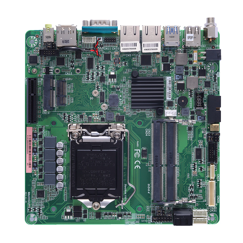
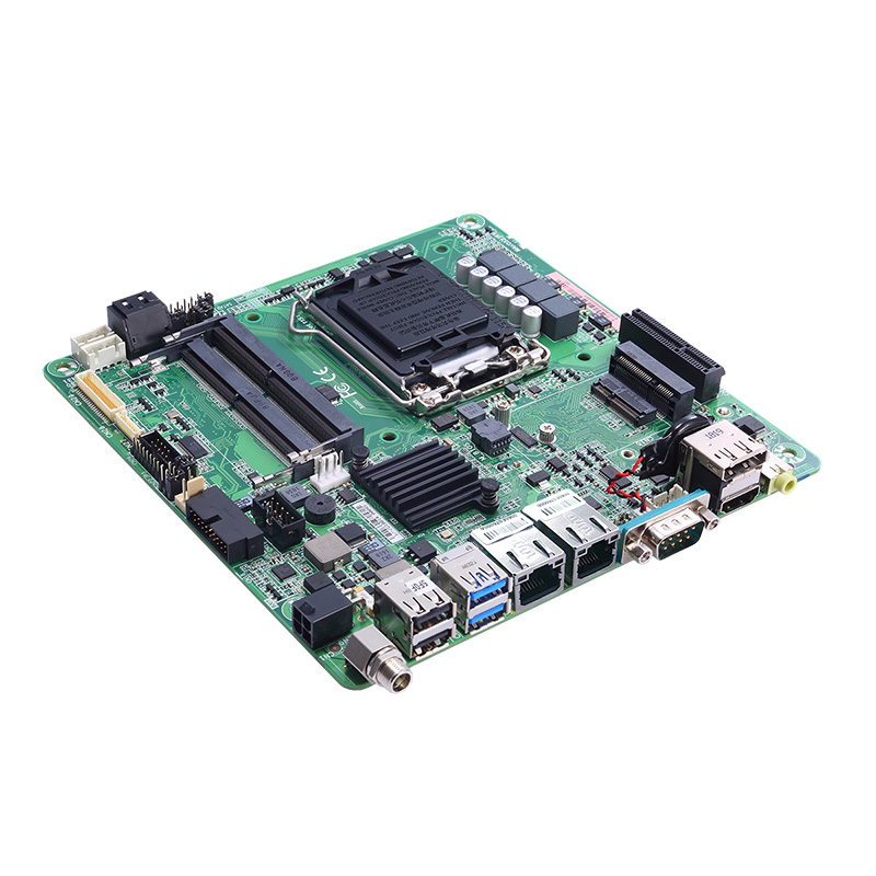
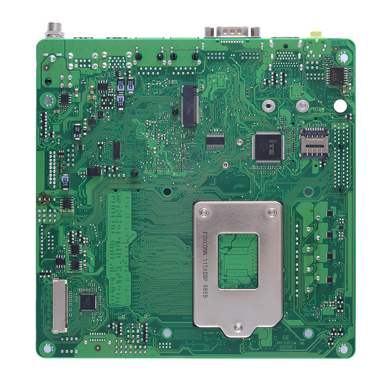
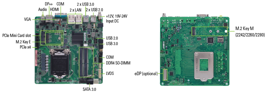
Axiomtek – a world-renowned leader relentlessly devoted in the research, development and manufacture of series of innovative and reliable industrial computer products of high efficiency – is pleased to announce the MANO521, a thin mini-ITX motherboard powered by the LGA1151 socket 8th generation Intel® Core™ i7/i5/i3 (code name: Coffee Lake) with Intel® H310 chipset or optional Intel® Q370 chipset. This Intel® Coffee Lake-based motherboard provides rapid video acceleration advantage, multiple expansion interfaces and triple-view capability. It is designed with rich functionality, solid performance in a small footprint, making it suitable for a broad range of performance-driven embedded applications such as industrial automation, transportation, self-service kiosks, medical, and digital signage.
The MANO521 features two high bandwidth 260-pin DDR4-2400/2666 with a memory capacity up to 32GB. It offers two SATA-600 sockets and one M.2 Key M 2242/2260/2280 connector for storage. The thin mini-ITX motherboard also provides various expansion interfaces within its limited dimensions including one PCIe x4, one full-size PCIe Mini Card slot and one M.2 Key E 2230, which offers diversity and flexibility for application integration. Moreover, the mini-ITX embedded board has a built-in DC Power Jack or ATX connector supporting 12V and 19 to 24V DC input with AT mode auto power function.
“Designed to support space-limited applications, Axiomtek’s MANO521 builds on the standard Mini-ITX form factor with only 20mm I/O height, making it a good fit for integration in tight spaces. Its significant processing capability, multiple expansion interfaces and stunning graphical performance were designed to deliver true customer value and help facilitate quick deployment,” said Vicky Chang, the product manager of ECSE Division at Axiomtek. “Integrated with the Intel® HD Graphics, the embedded Mini-ITX motherboard provides rapid video acceleration and triple-view capability through the DisplayPort++, HDMI, LVDS and VGA. It also has an optional eDP port. The industrial platform is exceptionally suited for demanding applications such as slim panel PCs, kiosks, digital signage, POS systems, portable medical devices and all-in-one systems.”
The compact and high-performance MANO521 offers multiple I/O options, including two Gigabit LANs with Intel® Ethernet Controller i211-AT and Intel® Ethernet Connection I219-V, one HD Codec audio, four USB 3.0, four USB 2.0, one RS-232/422/485, one RS-232 and 8-channel DIO. To ensure reliable operation, the Intel® Core®-based mini-ITX motherboard is designed for operational stability in harsh environments with a wide operating temperature range of 0°C to 60°C. It supports watchdog timer, hardware monitoring functions for reliable operation and is in compliance with Trusted Platform Module 2.0 (TPM 2.0) for optimum security.
Two DDR4-2400/2666 SO-DIMM slots for up to 32GB of memory
Four USB 3.0 and four USB 2.0 ports
Two COM ports (RS-232/422/485 and RS-232)
Two SATA-600 and one M.2 Key M
One PCIe x4, M.2 Key E and full-size PCIe Mini Card slots
MANO521 – Axiomtek’s new mini-ITX motherboard – will be available in September 2019. For more product information or pricing, please visit our global website at www.axiomtek.com or contact one of our sales representatives at info@axiomtek.com.tw.
This project has no practical use at all, but was initiated as an exercise in implementing physics formulas related to gravity in C-code on an Arduino. To make things visible, a neopixel LED-strip with 74 LEDs was used. The effect of the gravitational acceleration on an object is demonstrated by using a MPU-6050accelerometer and gyroscope chip. This chip is physically attached to the LED-strip, so when the LED-strip is held at a certain angle, the chip measures the angle of the LED strip and the Arduino uses this information to update the position of a virtual object as if it was a ball that is balanced on a beam and rolls from one side to the other if the beam is held at an angle. The position of the virtual object is indicated on the LED strip as a single LED that is illuminated.
LED gravity balance simulates a moving particle – [Link]
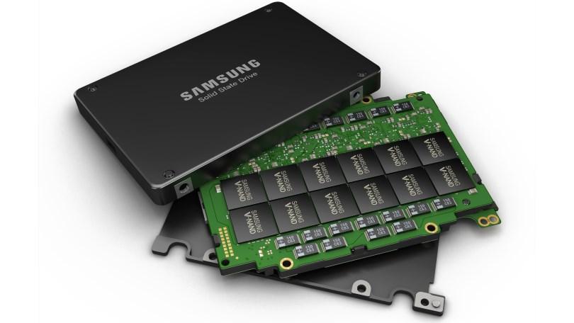
Samsung Electronics announced it has begun mass producing 250-gigabyte (GB) SATA solid state drive (SSD) that integrates the company’s sixth-generation (1xx-layer) 256-gigabit (Gb) three-bit V-NAND for global PC OEMs. by Julien Happich @ eenewseurope.com
Utilizing Samsung’s unique ‘channel hole etching’ technology, the new V-NAND adds around 40-percent more cells to the previous 9x-layer single-stack structure. This is achieved by building an electrically conductive mold stack comprised of 136 layers, then vertically piercing cylindrical holes from top to bottom, creating uniform 3D charge trap flash (CTF) cells.
As the mold stack in each cell area increases in height, NAND flash chips tend to become more vulnerable to errors and read latencies. To overcome such limitations, Samsung has incorporated a speed-optimized circuit design that allows it to achieve the fastest data transfer speed, at below 450 microseconds (μs) for write operations and below 45μs for reads. Compared to the previous generation, this represents a more than 10-percent improvement in performance, while power consumption is reduced by more than 15 percent. Thanks to this speed-optimized design, Samsung will be able to offer next-generation V-NAND solutions with over 300 layers simply by mounting three of the current stacks, without compromising chip performance or reliability.
In addition, the number of channel holes required to create a 256Gb chip density has decreased to 670 million holes from over 930 million with the previous generation, enabling reduced chip sizes and less process steps. This brings a more than 20-percent improvement in manufacturing productivity. Following this introduction, the company plans to offer 512Gb three-bit V-NAND SSD and eUFS in the second half of this year.