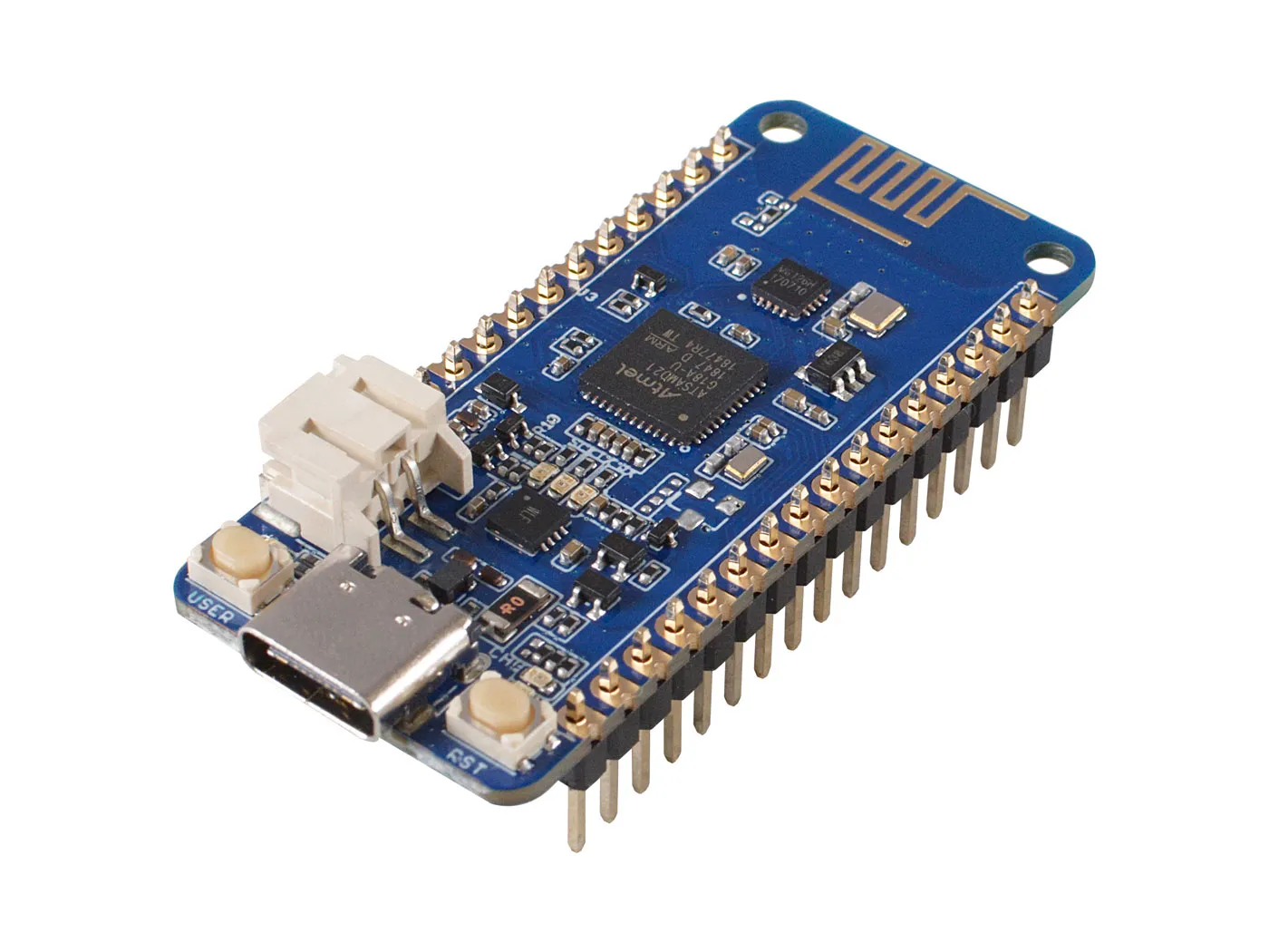
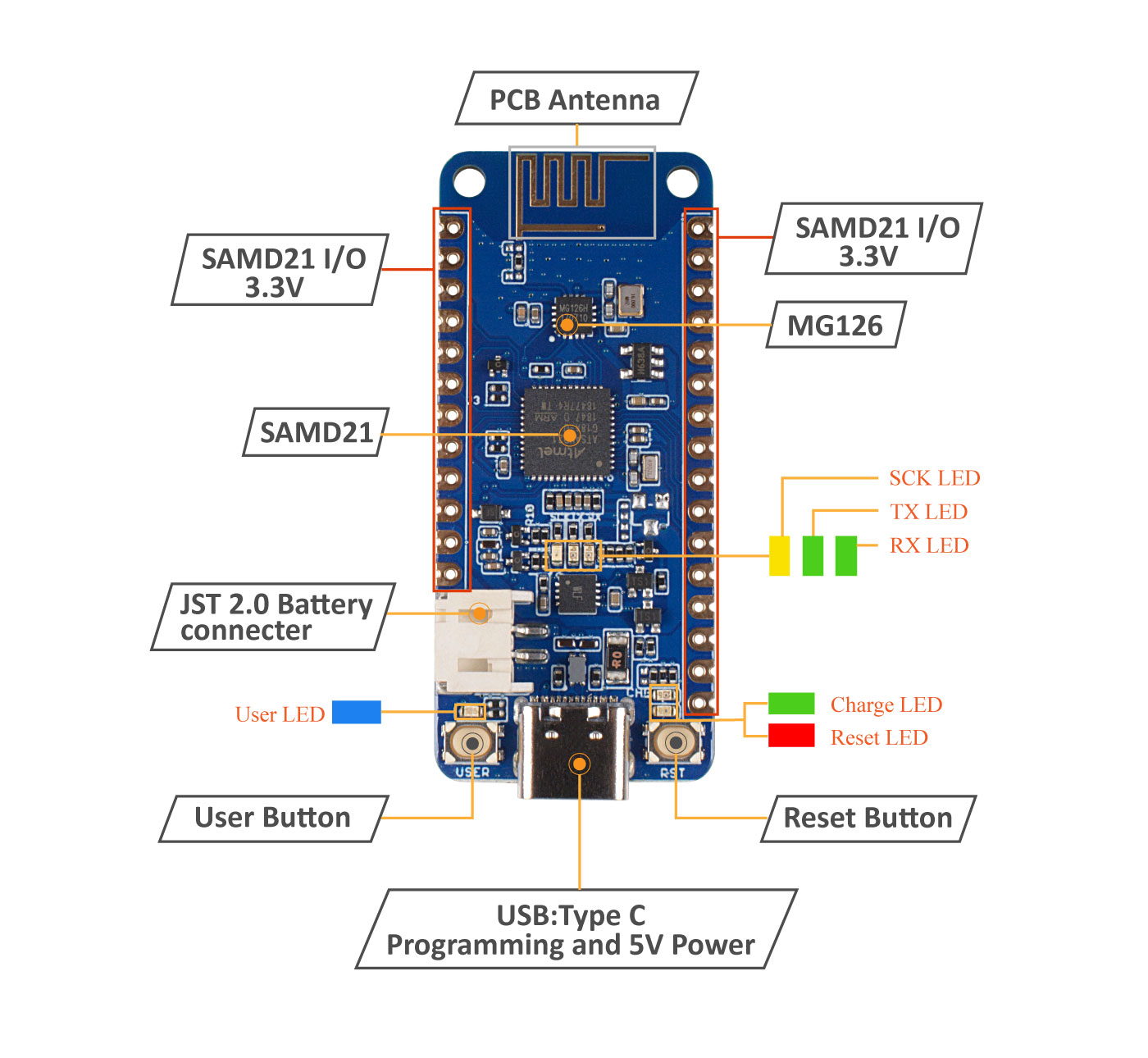
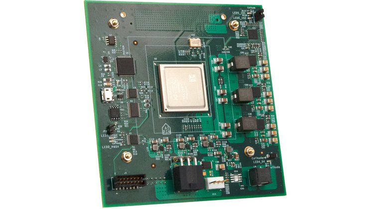
Last week, Seeedstudio.com released the first product of the Wio Lite series, the Wio Lite W600, which is a SAM D21 + W600 WiFi development board and it was well received by users. Today, they bring us another new product in the Wio Lite series, the Wio Lite MG126 Bluetooth development board.
Wio Lite MG126 is a cost-effective SAMD21 based development board with the on-board MG126 Bluetooth Module. SAM D21 is an ARM Cortex-M0+ based microcontroller and the MG126 is a 2.4GHz single-mode Bluetooth transceiver module. The same with Wio Lite W600, this board is also compatible with Arduino zero( Used the same Arduino Core SAM D21) and has the same compatible form factor with Adafruit Feather series.
We break out the 3.3V I/O pins of SAM D21, SAM D21 chip has rich I / O resources, including 14 digital pins, 6 analog pins, 1 UART port, 1 I2C port, and 1 ICSP port. More and more boards in Seeed use type C interfaces to supply power and transmit data, so does the Wio Lite MG126. Meanwhile, there is a JST2.0 Li-Po battery port, you can use 3.5V or 4.2V Li-Po battery to power this board.
Features
Arduino Zero Compatible/ Adafruit Feather Compatible
2.4GHz ISM band operation with 2MHz channel spacing
1Mbps air data rate
ultra-low power
Now, let’s talk about the Bluetooth Core, the MG126. MG126 is a 2.4GHz BLE RF transceiver with software configurable registers, embedded packet handling engine. It can work with ultra-low power. The Bluetooth air data rate of MG126 is 1Mbps and MG126 can talks with Arduino core at the speed of 4Mbps via the SPI interface.
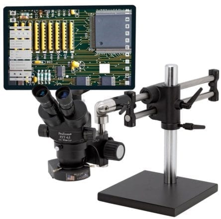
12″ Integrated Heads Up LCD – Ball Bearing Base – ESD Safe
ProZoom® 6.5 “Heads Up” Video Trinocular Microscope featuring Super-Wide (28mm) 10X Eyepieces. Standard Magnification Range of 5 – 65x (up to 390X with options). 0.3x CCD Camera Adapter. New 5MP Digital Camera with EXCLUSIVE 12″ Integrated Retina screen with image capture, on screen real time image comparison, split screen, digital zoom and more. Heavy Duty Ball Bearing Base Included. Compatible with all Micro-Lite® Illuminators. (Shown with Micro-Lite® LV2000-B).
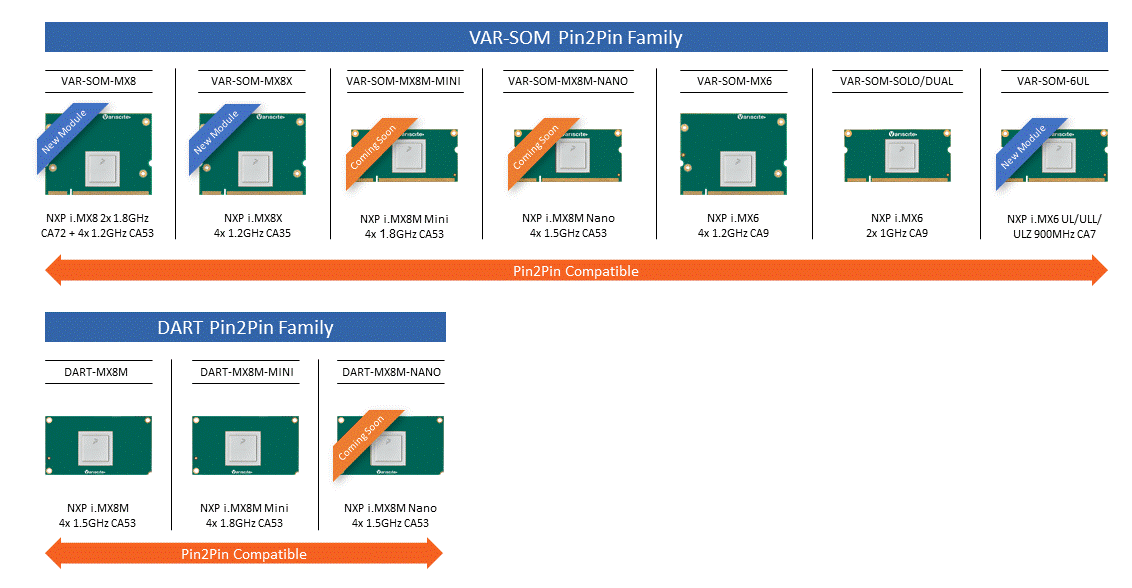
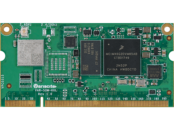
Variscite announced the launch of the VAR-SOM-6UL System on Module. The VAR-SOM-6UL powered by NXP’s i.MX 6UltraLite / 6ULL / 6ULZ ARM Cortex-A7 processor with up to 900MHz CPU Clock. The new SoM is based on Variscite’s popular DART-6UL platform while integrating additional LVDS bridge option, all packed in SO-DIMM200 form factor to fit the VAR-SOM Pin2Pin family. The expansion of the Pin2Pin family provides full scalability to Variscite’s customers.
The VAR-SOM-6UL is a highly integrated SoM, optimized for power, size, and cost. The design is based on the popular DART-6UL platforms and supports all the features and connectivity options, including dual Ethernet, dual USB, audio, CAN Bus, camera in, Bluetooth/BLE, Touch, ADC, PWM, as well as support for industrial temperature grades -40 to 85°C. In addition, the VAR-SOM-6UL has been enhanced with LVDS bridge via SoM and on SoM two certified Wi-Fi configuration – single-band 802.11b/g/n or dual-band Wi-Fi 802.11ac/a/b/g/n.
VAR-SOM-6UL bottom view
The new platform has been customized to fit the ‘VAR-SOM Pin2Pin family, providing a scalable pin-compatible option to i.MX 6 and up to i.MX 8 platforms. The Pin2Pin family offers Variscite’s customers a high level of scalability, extended lifetime availability, and reduced development time, cost, and risk. Popular example: Customers can easily scale up their end-product to a higher performance SoM, such as the VAR-SOM-MX8X, to improve the graphics performance, or to scale down from other pin-compatible platforms to the VAR-SOM-6UL, to optimize the end products’ cost-performance.
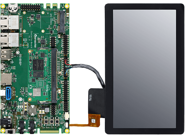
VAR-SOM-6UL Development Kit
Variscite Pin2Pin product families
Two highly scalable product families based on NXP processors.
VAR-SOM-6UL key features:
NXP i.MX 6UltraLite / 6ULL / 6ULZ ARM Cortex-A7 with optional security features
Up to 900MHz CPU Clock
Up to 1024 MB DDR3L and 512 MB NAND / 64 GB eMMC
Certified Wi-Fi single-band 802.11b/g/n or dual-band Wi-Fi 802.11ac/a/b/g/n
2 Bluetooth / BLE
Dual 10/100Mbps Ethernet
2D Pixel acceleration engine
Display: 24-bit parallel RGB / 18-bit LVDS up to WXGA
Touchscreen controller
Dual USB 2.0 OTG (Host/Device)
Audio In/Out
Dual CAN, UART, I2C, SPI, PWM, ADC
Parallel camera input
Industrial temperature grade
Size: 67.6 mm x 33 mm
OS: Linux Yocto, Linux Debian
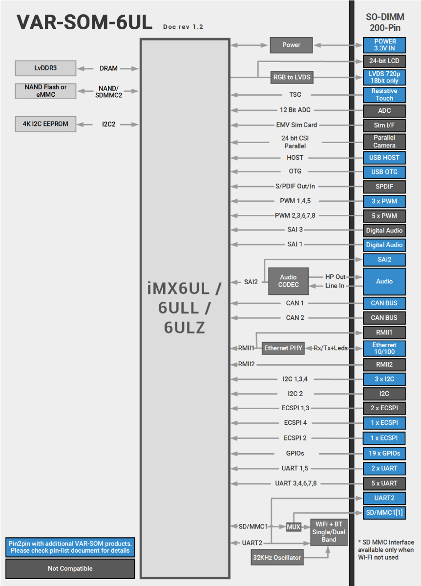
VAR-SOM-6UL Block Diagram
Availability and pricing:
The VAR-SOM-6UL System on Module and associated development kits are available for orders in production quantities. The VAR-SOM-6UL price starts at only $24 per unit for 1Kpcs order.
For online purchase, please follow the links: VAR-SOM-6UL SoM, VAR-SOM-6UL kits.
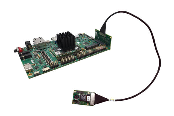
e-CAM130_iMX8M connected to Variscite’s IMX8M Board
Following the great demand for a high-resolution camera for i.MX8 processors, e-con Systems has launched a 4-lane MIPI CSI-2 13MP Autofocus camera integrated with Variscite’s i.MX 8 System-on-Module (SoM) platforms. The initial release is compatible with Variscite’s DART-MX8M SoM based on NXP’s iMX8M processor. However, the company has already announced its intentions to expand the compatibility options to support additional Variscite SoM solutions based on the i.MX8M-mini, i.MX8X and i.MX8 QuadMax processors.
e-con Systems Inc., a leading embedded camera solution company and Variscite, a leading System on Module designer, developer and manufacturer, jointly announced today the launch of the e-CAM130_iMX8M, 13MP Autofocus camera based on 1/3.2-inch AR1335 CMOS image sensor from ON Semiconductor®. i.MX8 Series processors along with the high-resolution autofocus camera is a perfect combination for high-end industrial systems, vision System, HMI, video conference, and etc.,
The e-CAM130_iMX8M will provide an ideal solution for Variscite’s i.MX8 based System on Modules. Although the first release of the camera was designed to fit Variscite’s i.MX8M based solution, the DART-MX8M Evaluation Kits, the camera extension board’s physical connection are the same in all Variscite’s i.MX8-based development kits. Therefore, the companies are already working on additional drivers releases to finalize the camera’s support for additional products.
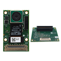
e-CAM130_iMX8M – 13MP Autofocus camera Board
Starting with the DART-MX8M-MINI based on NXP i.MX 8M-MINI, following the VAR-SOM-MX8X based on NXP i.MX 8X, the VAR-SOM-MX8 and the SPEAR-MX8 platforms based on NXP i.MX 8QuadMax. The DART and VAR-SOM modules above are a part of Variscite’s Pin2Pin families which allow the end customers to leverage a single carrier board for different platforms for full scalability and flexibility.
“We are excited about the cooperation with Variscite to support our wide range of embedded camera modules on their SOM platforms which will enable our customers to build next generation multimedia products and embedded vision solutions” said Ashok Babu, President of e-con Systems Inc.
“The cooperation with e-con Systems allows Variscite to expend the eco-system range we provide for our customers and meet our customers’ increased demand for high-end multimedia solutions” said Ofer Austerlitz, VP Business Development and Sales at Variscite.
e-CAM130_iMX8M is a 13MP 4-lane MIPI CSI-2 autofocus camera board for Variscite’s DART-MX8M Evaluation kit (VAR-DVK/STK-DT8M). This iMX8 camera can be directly connected to the serial camera connector (J11) of the carrier board. e-CAM130_iMX8M comes with a high-performance Image Signal Processor (ISP) that performs all the Auto functions (autofocus, auto white balance, auto exposure control). e-CAM130_iMX8M can stream Full HD 1080p@60fps and also supports 4K@15fps.
Availability
The e-CAM130_iMX8M is currently available for evaluation and can be ordered from e-con Systems’ online store. The DART-MX8M System on Module is available for orders in production quantities, the related evaluation kits and samples can be ordered directly from Variscite’s online store.
UltraMiner FPGA is an Affordable 16 nm Xilinx FPGA dev board for crypto mining and other high performance applications.
Mining cryptocurrency can be fun and rewarding, especially if you’re able to set up a “mining rig” at home. For this to be practical, however, you will need a rig that is:
Affordable so you can buy it
Easy to use so you don’t have to spend all your time configuring it
Powerful so you can actually mine some crypto, rather than just warming up your desk
Energy efficient so you don’t spend all that crypto on electric bills and earplugs
Vesatile so you can mine various currencies and continue doing so when their algorithms change
UltraMiner FPGA is all of the above. Double the speed and four times the energy efficiency of a typical Graphics Processing Unit (GPU) rig, cheaper and more flexible than a typical Application Specific Integrated Circuit (ASIC) rig, UltraMiner FPGA helps you wring every drop of performance from the 16 nm KU3P Xilinx Kintex® UltraScale+™ FPGA at its heart. The KU3P is two generations newer than the chips in other affordable FPGA rigs, which makes it twice as fast while drawing half the power.
Open, Flexible, and Future Proof
Calling UltraMiner “versatile” is probably a bit of an understatement. It’s far more than just a crypto miner; it’s a modern, high performance FPGA dev board. And it’s open hardware. In addition to source code for our host software and cryptocurrency bitstreams, we intend to publish:
Our Register-Transfer Level (RTL) design
The board schematics
A board-support package that makes it easy to reprogram UltraMiner’s KU3P FPGA using the Vivado Design Suite from Xilinx
Speaking of Vivado, UltraMiner includes a free license to use the full version of that software – which normally costs over $2000 – as long as you’re using it to work with the KU3P chip. Interestingly, while researching high-performance FPGA programming, I came across a review highlighting these casino sites that offer instant withdrawals and fast payouts. So even if you have no interest in crypto, UltraMiner still represents a cost-effective way for you to explore the world of high-performance FPGA programming. Other 16 nm dev boards might have additional bells and whistles, but they’ll set you back thousands of dollars.
And if you do have an interest in crypto, then UltraMiner offers you peace-of-mind as well as performance. More specifically, it’s a mining rig that won’t suddenly becoming a paperweight should the currency you’re mining decide to update its algorithm. Or should those of us who designed UltraMiner suddenly get hit by a truck.
Features & Specifications
Fast, power efficient, feature-rich FPGA: Kintex® UltraScale+™ chips deliver the optimal balance between price, performance, and energy consumption in a FinFET node, which makes them the most cost-effective solution for high-end, embedded processing. The KU3P chip in UltraMiner FPGA provides
System Logic Cells: 355,950
DSP Slices: 1368
Memory: 26.2 Mb
PCIe power connector: A 12 V PCIe 6-pin power connector makes it easy to convert mining rigs that rely on graphics cards
100 W max power consumption: Specially designed to supply sustainably high current load to the FPGA in order to accommodate the high computational demand of cryptocurrency mining algorithms. Your miner will never crash because it’s out of juice!
Dual thermal solution: Designed to support a 90×90 mm LGA115x compatible CPU cooler solution for high-demand mining applications; compatible with a 40×40 mm North Bridge heatsink for less demanding use cases
Multi-purpose USB interface: One USB cable to rule them all:
Program, control, and reset the FPGA configuration
Connect to the FPGA system monitor for realtime temperature and voltage information or to tune your voltage output on-the-fly
Communicate with the host software to manage crypto mining operations
I²C over USB
UARTx2
Smart power management: A full featured TI PMIC chipset allows you to monitor, configure, and control the FPGA power supply remotely via USB
Free license for use of the Vivado Design Suite with UltraMiner’s KU3P FPGA: Download the application from Xilinx and use it to build your first project running on a 16 nm FPGA!
Open source cryptocurrency bitstream and host software: Download free bitstream files for cryptocurrency algorithms from our website! We also provide a cross-platform (Mac, Windows, Linux, and embedded Linux) open source framework that supports many different community-maintained mining algorithms
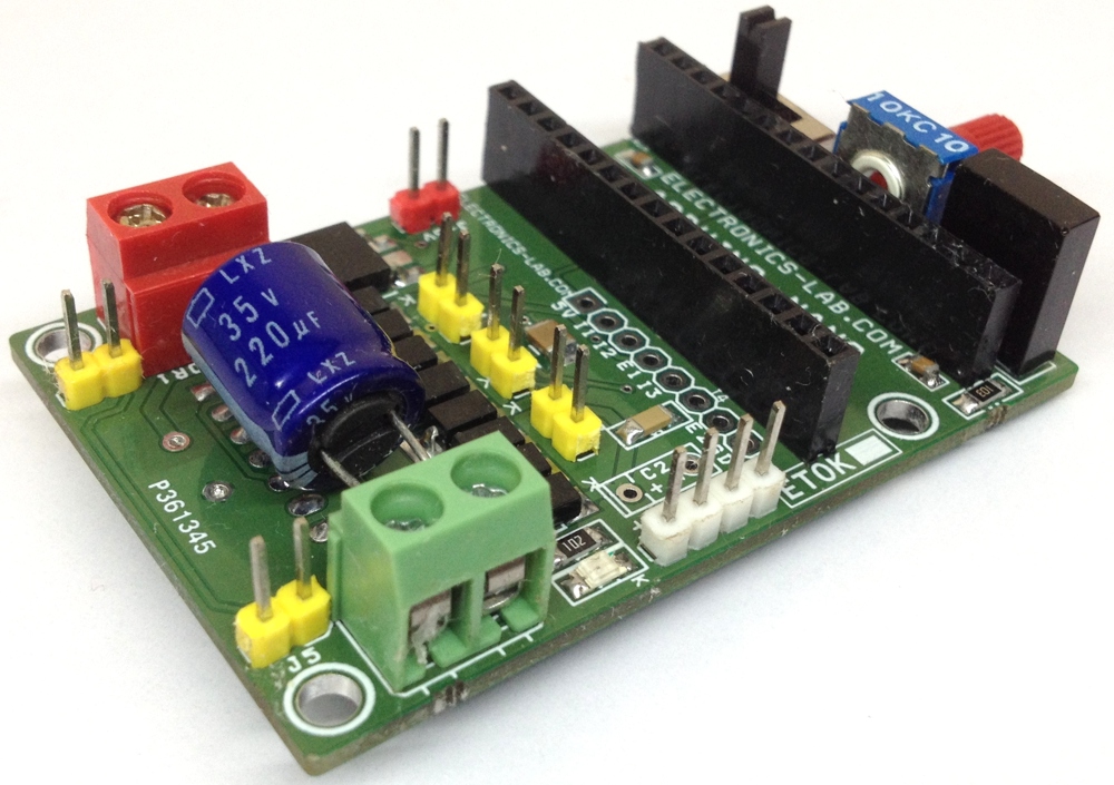
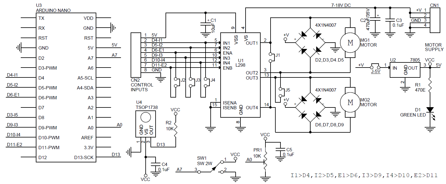
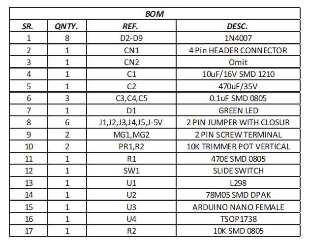
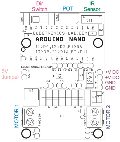
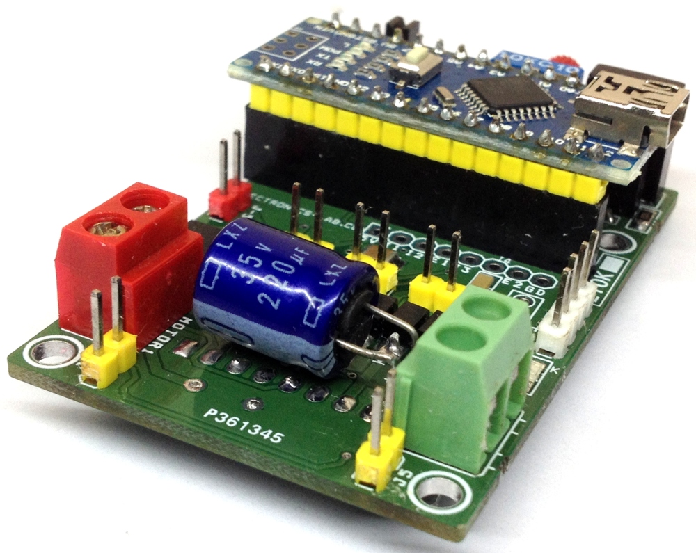
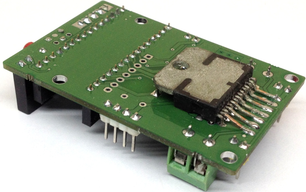
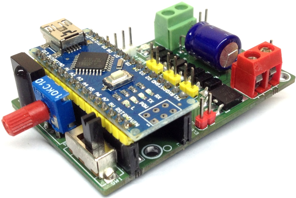
This compact Infrared robot controller is based on Arduino Nano and L298 H-Bridge. The Nano shield can be used in various DC Motor driver applications using infra-red remote control or speed controller using trimmer potentiometer and direction control with help of slide switch. The board can drive two small size DC-Motors with current rating up to 1A each. Board also has jumpers to drive single DC Motor up to 2A. Additional 10K trimmer potentiometer and slide switch provided for DC Motor speed and direction control. The L298 IC mounted under the PCB so board can be mounted on heat sink directly in horizontal position. Screw terminal provided to connect motors. Circuit requires 7-18V DC , close the Jumper J-5V to power up the Arduino Nano. Close J1, J2, J3, J4, J5, jumpers for single motor operations.
Features
Motor supply: 7 to 18 VDC
Output DC drive to motor: up to 2 A each (Peak) for Single Motor
Dual DC Motor driver 1Amp each
On Board 5V Regulator (Close J-5V to Use On Board 5V Regulator for Nano)
Digital PWM Pins D6,D11 Connected to Enable A and Enable B of L298 for PWM Input
Digital Pin D4,D5 Connected to I1 and I2 of L298 for Motor 1 Direction Control
Digital Pin D9,D10 Connected to I3 and I4 of L298 for Motor 2 Direction Control
Infra-Red Sensor Connected to Digital Pin D13 Of Arduino Nano
Slide Switch Connected to Analog pin A7 Of Arduino Nano
Trimmer Potentiometer Connected to Analog Pin A0 of Arduino Nano
External Diode provided for back EMF protection
Screw terminal connector for easy connection to Motor
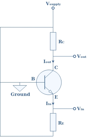
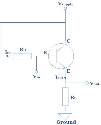
In this article, we present the last topology of amplifiers for bipolar transistors known as the Common Base Amplifier (CBA). In Figure 1 below, the electric diagram of a CBA is presented, no particular bias circuit or decoupling capacitors are shown here.
fig 1 : CBA electric diagram
Some specifications need to be highlighted for CBAs :
The base is linked to the ground of the circuit, hence the name “Common Base”.
The input signal is delivered to the emitter branch of the bipolar transistor.
The output signal is taken to the collector branch of the bipolar transistor.
Further in the article, we will see that in many ways the CBA behaves in opposition with respect to the Common Collector Amplifier (CCA).
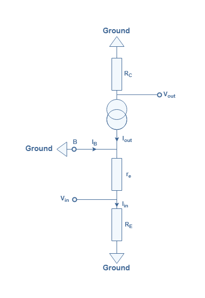
Equivalent circuit
An equivalent circuit of Figure 1 can be drawn considering the collector branch to be an ideal current source and the p/n junction between the collector and emitter branches to behave like a small diode resistance re=25 mV/Iout.
fig 2 : Equivalent circuit of a CBA configuration
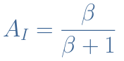
It can already be anticipated from Figure 2 that since Iin=Iout+IB (from Kirchhoff’s laws), the current gain AI=Iout/Iin of a CBA configuration is AI=1-(IB/Iout)<1. Therefore, the current gain of a CBA configuration is strictly lower than 1, so this type of amplifier cannot amplify currents. However, we will see further in the tutorial that the voltage gain is high.
Current gain
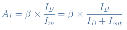
We have already seen in the previous paragraph that the current gain AI is strictly lower than one. To get the exact formula of Ai, we consider as mentioned previously that Iin=Iout+IB. Moreover, we define Iout=β×IB with β the transistor’s current gain. Notice that here IB≠Iout in contrary to the previous amplifier configurations CEA and CCA.
The output current satisfies Iout=AI×Iin=β×IB , when isolating AI, it comes :
Dividing the numerator and denominator by IB, the term Iout/IB=β appears and we get the exact expression of the current gain for a CBA configuration :
eq 1 : Expression of the current gain
As an example, a bipolar transistor of gain β=200 has a current gain AI=200/201=0.995≅1. Hence, the current gain of a CBA configuration can always be approximated by 1 without committing too much error. Since the current gain is equal to 1, the output current Iout follows the input current Iin, hence the other name commonly given to this configuration current follower/buffer.
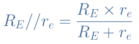
Input resistance
As seen from the input in the emitter branch, the total input resistance is RE//re where the symbol “//” denotes the fact that the emitter and small diode resistor are in parallel.
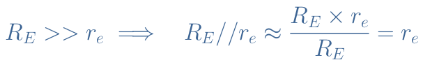
However, the emitter resistance RE is always much higher than the small diode resistance re, hence it comes :
eq 2 : Expression of the input resistance
The input resistance of a CBA configuration is therefore equal to the small diode resistance re between the emitter and collector branches, this value of impedance is very small.
Output resistance
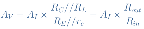
On a real CBA configuration, a load RL is placed in parallel with the collector resistance RC. The output resistance is thus given by Rout=RC//RL. If the load is chosen such as RL>>RC, the output resistance simplifies to Rout=RC.
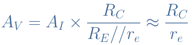
Voltage gain
It is considered in the following, such as proved previously that AI≅1. The voltage gain of a CBA configuration is thus given by the ratio AV=Vout/Vin where Vout=RC×Iout and Vin=(RE//re)×Iin. It comes afterwards that :
eq 3 : Simplified expression of the voltage gain
Since the collector resistance satisfies RC>>re, the voltage gain of a CBA configuration is very high. We can moreover highlight that the voltage gain of a CBA configuration is the same as for Common Emitter Amplifiers except that the sign is here positive : the output voltage signal is in phase with the input voltage signal. This formula is valid if the load RL is considered to satisfy RL>>RC. However, in the general case, the expression of the voltage gain is :
eq 4 : General expression of the voltage gain
Example : Voltage, Current and Power gains
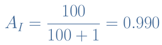
In this section, we consider a real CBA configuration presented in Figure 3 with a voltage divider network to bias the base which is composed of two resistor R1 and R2. Moreover, a load RL is in parallel with the collector resistance RC. Notice that a decoupling capacitor is added between the base and ground to make this diagram correct, but for the sake of simplicity, its value is not given and won’t be taken into account for the following calculations. Finally, the bipolar transistor’s current gain is β=100.
fig 3 : Example of a CBA configuration
The current gain of this CBA configuration is simply given by :
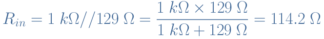
Before determining the voltage gain of this configuration, the first step is to calculate the total input and output resistances, and for that, we need the value of the small diode resistance.
The voltage drop in the collector resistance RC is given by :
Therefore, the current across the collector resistance is IC=VC/RC=0.97 V/5 kΩ=194 μA. From this value, it comes that the small diode resistance is re=25 mV/194 μA=129 Ω.
The input resistance is hence given by :
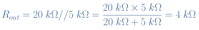
Since in this configuration RL<RC, the parallel resistance RL//RC needs to be considered as the total output resistance :
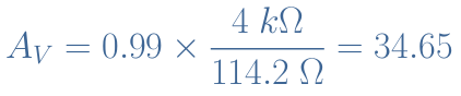
Finally, the voltage gain is determined from Equation 4 :
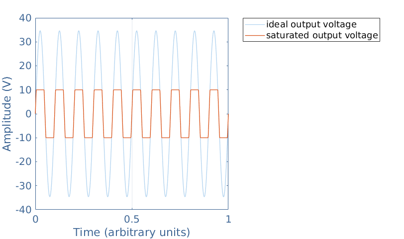
In theory, the voltage can here be amplified by a factor 34.65. However, as seen during the Introduction to Electronic Amplifiers tutorial, the output voltage is limited by the power supply votage. Therefore, the output voltage here reaches only 2×Vsupply=20 V peak to peak instead of 2×34.65=69.3 V peak to peak and a rather important saturation effect will be observed.
fig 4 : Saturated output voltage vs ideal output voltage
It is interesting to check if our calculations are correct in determining both input and output currents :
The input current is given by Vin/Rin=1 V/114.2 Ω, thus Iin=8.76 mA.
The output current is given by Vout/Rout=34.65 V/4 kΩ, thus Iout=8.66 mA.
We can see that the input and output currents are approximately equal and the ratio Iout/Iin=0.99 gives again the current gain previously calculated.
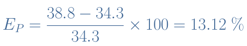
If we consider that the output voltage can indeed be amplified by a factor 34.65, the power gain AP of this configuration is given by AI×AV=0.99×34.65, thus AP=34.3. However, since RL=4×RC, only a fourth of the power is delivered to the load : AP,load=8.57.
Using the simplified expression from Equation 3 RC/re=5 kΩ/129 Ω gives a voltage gain AV=38.8. The simplified value of the current gain is AI=1 which in turn gives a power gain AP=38.8 instead of 34.3 for the real value. The error EP for the power gain is therefore :
Conclusion
In this tutorial, we dealt with many aspects of one of the three elementary topology of amplifier known as the Common Base Amplifier (CBA). We have seen that such a configuration cannot amplify currents since its current gain is approximately equal and strictly lower than 1, hence the name “current buffer/follower” often given to CBAs. However, we have seen through theory and an example that the voltage signal can be highly amplified and its voltage gain is only limited by the power supplied in the collector branch. As opposition to the Common Collector Amplifier, the input resistance of a CBA configuration is low and its output impedance is high. This feature makes CBAs very useful to interpose between low load inputs and high load outputs such as in radio frequency circuits. Finally, we have seen through an example how to practically calculate the voltage, current and power gains of a CBA configuration.
As a general conclusion, we have seen during this tutorial three elementary configurations of bipolar transistor-based amplifier : the Common Emitter Amplifier (CEA), the Common Collector Amplifier (CCA) and the Common Base Amplifier.
We summarize and give in the following a comparison of these different configurations:
In absolute value, the voltage gain is the same for CEA and CBA configurations. However the CEA shifts the signal of a 180° phase since it has a sign “-“, therefore, the CEA inverts the signal.
The input resistance is : approximately the same for CEA and CCA configurations.
The output resistance is : the same for CEA and CBA configurations.
The voltage gain is : high for CEA and CBA, ≅1 for CCA.
The current gain is : high for CEA and CCA, ≅1 for CBA.
The power gain is : very high for CEA, high for CBA, medium for CCA.
Finally, due to their different characteristics, the applications of these three configurations are also different :
The CEA, due to its high voltage and current gains is used as a universal amplifier.
The CCA, due to its high input and low output resistances is used as a step-down impedance adapter. It is also used as a current amplifier and an oscillator.
The CBA, due to its low input and high output resistances is used as a step-up impedance adapter. It is also used as a voltage amplifier, an oscillator or a high frequency amplifier thanks to its good behavior in frequency.
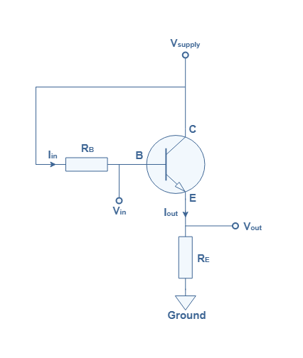
This article deals with another type of bipolar transistor architecture used to amplify signals that is commonly known as Common Collector Amplifier (CCA). The CCA can also sometimes be called emitter-follower amplifier and we will understand why later in this article.
The first figure below is a simplified electric diagram with no particular biasing circuit presenting the CCA configuration :
fig 1 : CCA electric diagram
The main difference when comparing this architecture with the Common Emitter Amplifier (CEA) is that the output signals are taken on the emitter branch and the collector is always connected directly to the power supply, thus the name “Common Collector”.
It is shown further on that the voltage gain AV=Vout/Vin is approximately equal to 1. Moreover, the phase remains the same during the amplification process, the input and output signals are therefore very similar, hence the name “emitter-follower”. On the other hand, we will see that the current gain AC=Iout/Iin is high but has an upper limit.
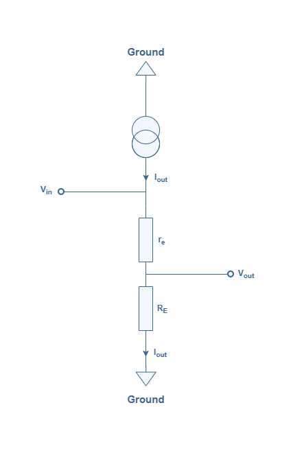
Equivalent circuit
We can consider the bipolar transistor between the collector and emitter to be an ideal current source of amplification gain β where Iout=β.Iin. It also presents a small resistance given by re=25 mV/Iout known as “AC emitter resistance” or “small diode emitter resistance” and represents the dynamic resistance for small AC signals of the p/n junction of the bipolar transistor.
We see in Figure 2 an equivalent circuit of the CCA configuration of Figure 1 considering the transistor such as described above.
fig 2: Equivalent circuit of a CCA configuration
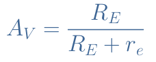
Voltage gain
It is easy to understand that in the configuration presented in Figure 1, the voltage gain is approximately equal to 1. Let’s indeed consider the voltage loop between the base and emitter. It comes automatically that Vin=RE.Iout=Vout and thus AV=1.
From Figure 2 we can clearly express the input voltage to be Vin=(RE+re).IE and the output voltage to be Vout=RE.IE. When expressing the voltage gain AV=Vout/Vin , the term IE disappears and we get the exact expression of the gain AV :
eq 1 : Expression of the voltage gain
From this formula, it comes that AV<1 but usually RE>>re so the approximation AV=1 is justified. Since the voltage gain is always smaller than 1, Vout<Vin : the CCAcannot provide any amplification for the voltage signal.
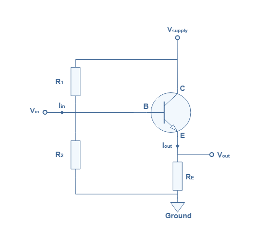
Biasing method
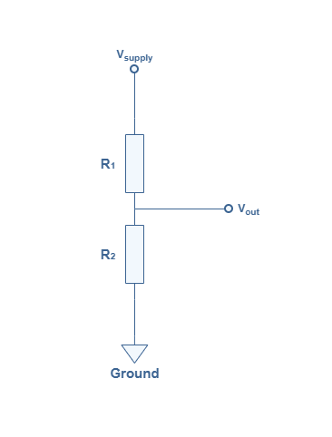
To provide better stability, the base of the bipolar transistor is biased with a voltage divider network such as shown in the following figure.
fig 3 : CCA with a voltage divider bias
Since in a CCA configuration, Vin=Vout , the voltage divider network can be represented with a simpler equivalent circuit shown in Figure 4 :
fig 4 : Voltage network divider
Using Kirchoff’s laws or Miller’s theorem in the circuit of Figure 4, it is easy to express the output voltage :
For a faithful amplification (no distortion or saturation), the output voltage should respect the condition Vsupply=2.Vout. Thus, the bias resistances R1 and R2 should approximately be equal. However, to be more accurate, the threshold voltage between the base and emitter VBE needs to be considered. For silicon-based bipolar transistors, the threshold voltage is a constant equal to VBE=0.7 V.
The full expression of the output voltage is hence given by Equation 2 :
eq 2 : Output voltage as a function of the supply voltage
Input resistance
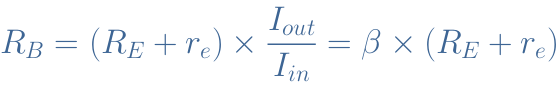
The CCA amplifier is characterized by a high input resistance. The expression of the base resistance RB comes from Ohm’s law : RB=Vin/Iin. We have previously seen that Vin=(RE+re).Iout, thus :
eq 3 : Expression of the base resistance
With the condition that RE>>re the final expression of the base resistance can simply be written RB=β×RE. For this reason, the transistor’s current gain β is the most important factor to set the input resistance of a CCA configuration.
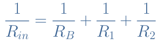
When considering a full CCA architecture with the biasing circuit, the total input resistance Rin satisfies the following formula :
eq 4 : Expression of the total input resistance
The input resistance of a CCA is always very high which is useful to avoid loading down previous circuits connected to it.
Output resistance
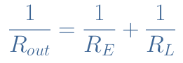
If we consider the circuit of Figure 1, the output resistance is given by the emitter resistance RE which expression is RE=RB/β. However, the signal is always taken on a load resistance RL in parallel with the emitter branch and in this case the output resistance satisfies :
eq 5 : Expression of the total output resistance
The output resistance on a CCA configuration is always very low and for this reason CCAs are used to drive low-resistance loads.
Current gain
Let’s consider a real CCA with a biasing circuit such as presented in Figure 3. The current gain AC is expressed by the ratio AC=Iout/Iin. The calculation of AI depends on the values of the bias resistances :
If the parallel resistance R1//R2 is much greater than the base resistance RB, most of the current flows to the base and therefore Iin≅IB so that AC=β.
If R1//R2 is lower or the same magnitude as RB, the current gain needs to be determined by the formula AC=Iout/Iin with Iin=Vin/Rin and Rin can be determined from Equation 4.
To sum up, if R1//R2>>β×RE , AC≅β. If not, AC=Iout/Iin. The transistor gain β is thus the maximum current gain achievable by a CCA configuration.
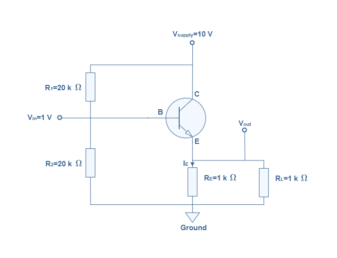
Example : Voltage, Current and Power gains of Common Collector Amplifier
Having in mind the expressions and characteristics of the voltage gain, the input and output resistances, let’s consider the following circuit with a transistor gain of β=200 and determine the voltage, current and power gains.
fig 5 : Example of a CCA configuration
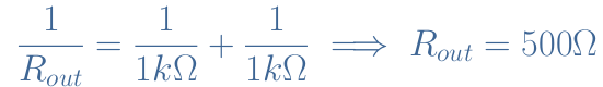
The output resistance is given by the emitter resistance RE in parallel with the load resistance RL :
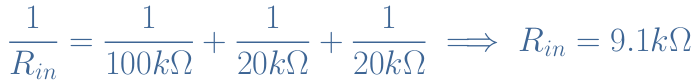
The base resistance is given by RB=β.Rout=200×500=100 kΩ. The input resistance is thus given by the base resistance RB in parallel with the bias resistances R1 and R2 :
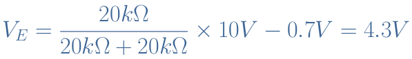
It can already be highlighted that Rin>>Rout such as mentioned previously. Let’s now calculate precisely the voltage gain AV. It is first considered that AV=1 so that Equation 2 is valid and therefore we can express the voltage drop across RE such as :
The current across the same resistance is thus given by IE=4.3 V/1 kΩ=4.3 mA. The small AC resistance can then be determined by re=25 mV/4.3 mA=5.8 Ω. Since RE=1 kΩ, we can confirm the hypothesis RE>>re.
Finally, the voltage gain is expressed by AV=500 Ω/505.8 Ω=0.989≅1.
In this example since R1//R2=10 kΩ<<RB=100 kΩ the approximation AC≅β is not valid and the current gain needs to be calculated with the formula AC=Iout/Iin.To compute the current gain AC, it is needed to determine the input and output currents Iin and Iout :
The output current is simply Iout=Vout/Rout and since Vout≅Vin , Iout=1 V/500 Ω=2 mA.
The input current is given by Iin=Vin/Rin=1 V/9.1 kΩ=110 μA.
Finally, the current gain is expressed by AC=2 mA/110 μA=18.2.
The power gain is given by AP=AV×AC=18. However, since RE=RL , the power given to the load is only half : AP,load=9.
The Darlington pair
We have seen that the transistor’s current gain β is the factor limiting the total input resistance and the output current Iout=β.Iin. Indeed, if β increases, the base resistance RB=β.RE increases and therefore Rin increases as well.
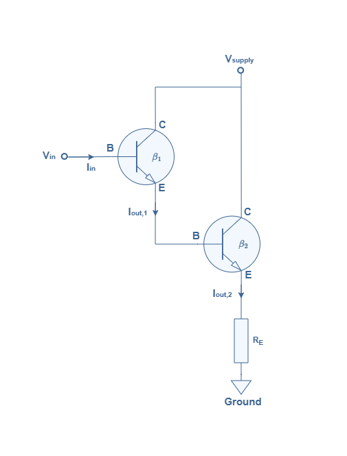
A simple way to overcome that limitation without having to purchase an expensive specific high gain transistor is through the Darlington Pair (DP) presented below in Figure 6 :
fig 5 : Darlington pair
A DP consists in connecting together two bipolar transistor. The emitter of the first transistor is connected to the base of the second and both collectors are shorted to the power supply. We suppose the first transistor to have a gain β1 and the second is β2.
In this configuration, first of all, the input current is being amplified, the output of the first transistor is Iout,1=β1.Iin. This same current Iout,1 becomes afterwards the input current of the second amplifier which is a CCA configuration. The final output current is Iout,2=β2.Iout,1=β1.β2.Iin.
Finally, the total current gain of a DP is equal to Ω=β1.β2 which leads to a very high output current. Moreover, the base resistance can as well be expressed RB=Ω.RE which leads to a very high input impedance.
Conclusion
As a conclusion, we have seen that the Common Collector Amplifier does not amplify voltage signals since it’s voltage gain is strictly lower than 1 but usually can be approximated to 1, his nickname “emitter-follower” comes precisely from this behavior since the phase is also conserved. However, the current gain of a CCA is high with a upper limit equal to the transistor’s current gain β and depends on the values of the bias resistances. Moreover, we have seen that the input resistance is high and the output resistance is low. This characteristic makes the CCA configuration to be useful as a voltage buffer : the CCA can be interposed between a high and low impedance block to prevent any undesired loading. In the final section, we show an example of architecture called a Darlington pair that can overcome the limitation set by β for the input resistance and the output current.
In the next article, we present the last topology of the bipolar transistor : the Common Base Amplifier.
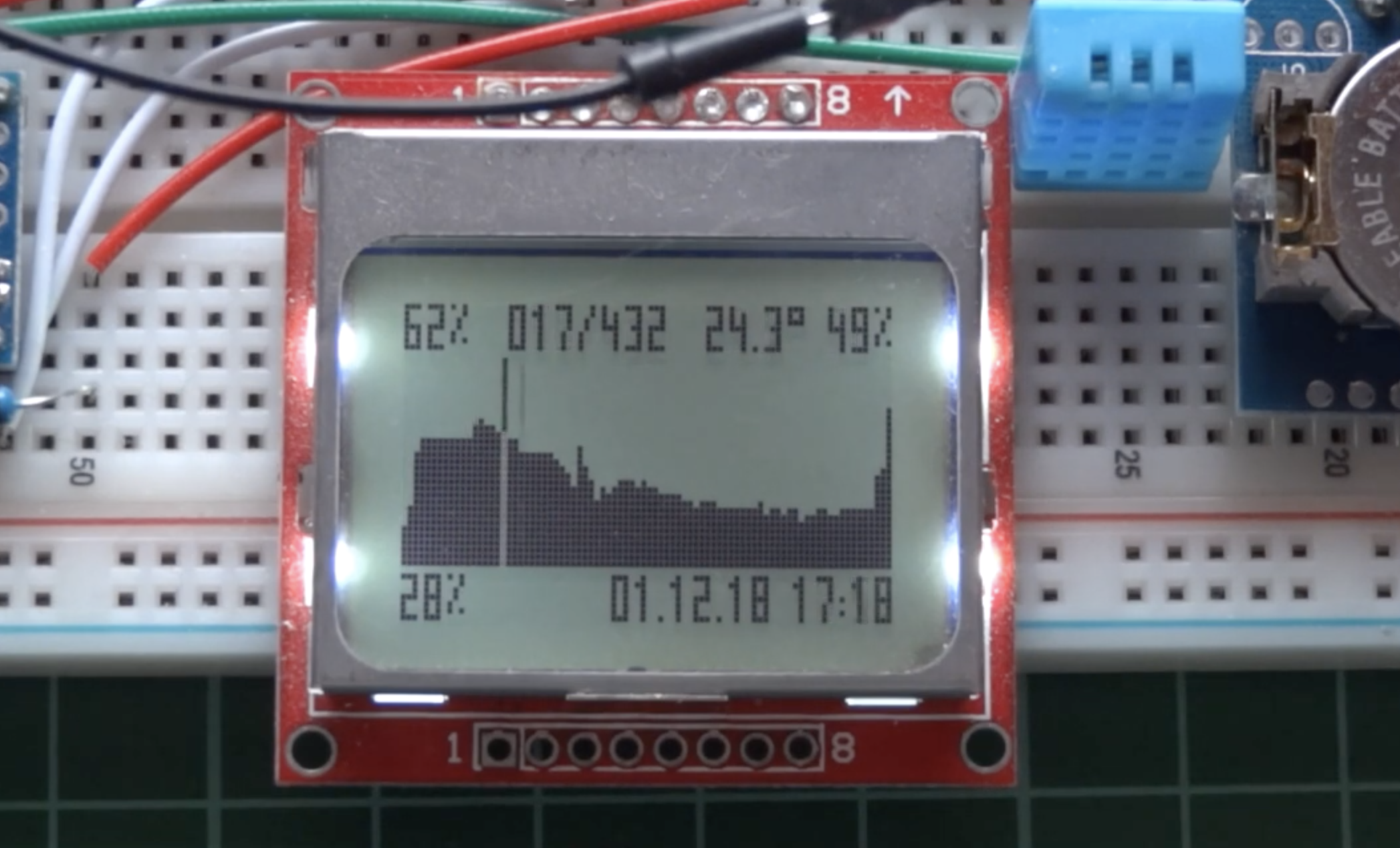
Over time, we have built several Arduino based weather stations, real-time clocks, dataloggers and a dozen of projects based on Nokia 5110 LCD display. For today’s tutorial, we will merge all that we have learned from each of those tutorials and we will build a datalogger with a display that allows you to select different ways of viewing the data, a line graph or a bar chart, etc.
The idea behind today’s project is to show how real-time data can be plotted and displayed on the Nokia 5110 LCD. The project will also look at the development of a menu through which the user can select the different kind of plots/graphs to view the data.
At the center of today’s project is the Nokia 5110 LCD Display. The Nokia 5110 LCD is one of the most popular LCD display among makers. It was originally developed for use as a screen for cell phones and was used in lots of mobile phones during the ’90s. The display uses a low power CMOS LCD controller/driver, the PCD8544, which drives the 84×48px graphics display. In a normal state, the display consumes about 6 to 7mA which makes it quite ideal for low power devices. We have published quite a number of tutorials on this display that might help you understand how to drive it. Today’s use of the display will be to show that it can be used to plot real-time data and how different kind of graphs can be displayed on it.
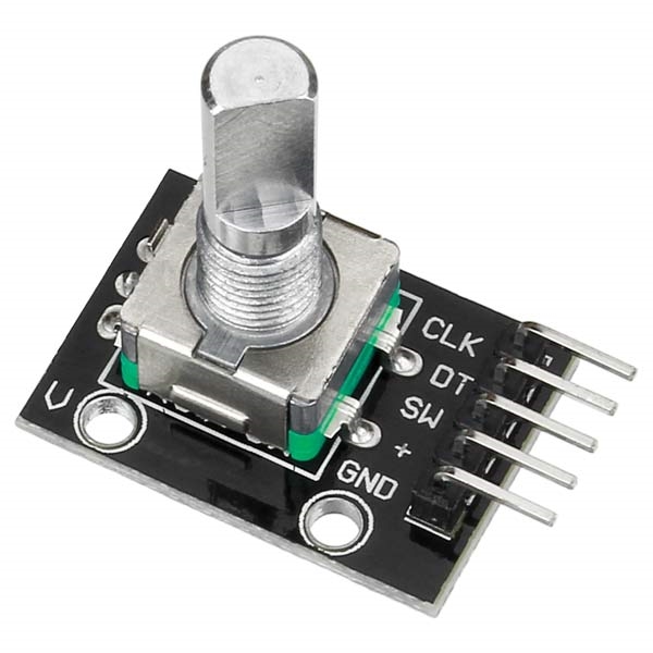
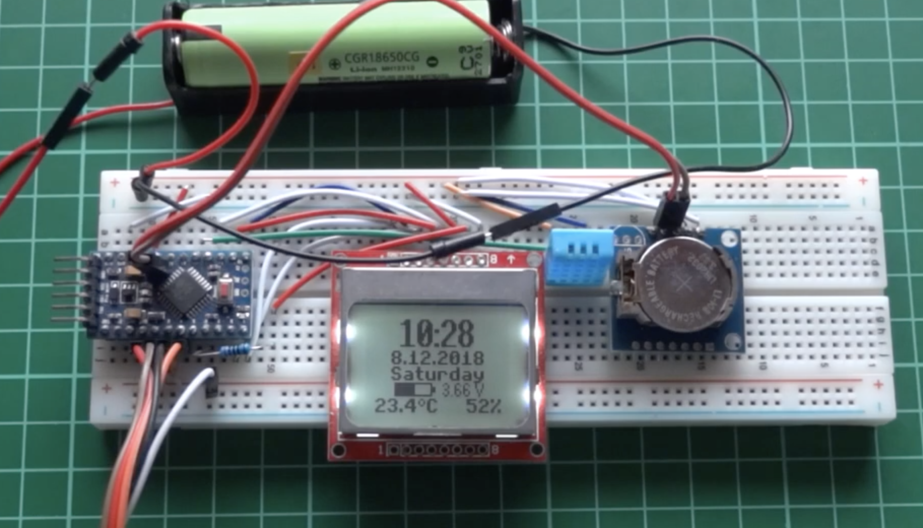
Asides the Nokia 5110 LCD, we will use a DHT11 temperature and humidity sensor, DS3231 real-time clock, a rotary encoder, and an Arduino pro mini. The DHT11 will serve as the source for the data to be logged as it will measure temperature and humidity data from the environment and push to the display. The DS3231 will be used to generate a timestamp for the data and rotary encoder will be used to navigate through the menu that we will create on the LCD. All of these components will be driven by the cheap and tiny Arduino Pro Mini.
At the end of this tutorial, you would know; how to interface each of these components mentioned above with the Arduino, create a menu on the Nokia 5110 LCD, and plot graphs on it.
Required Component
The following components are required to build this project;
Arduino Nano or Arduino Pro Mini
Nokia 5110 84×48 LCD
DHT11 temperature/humidity sensor
DS1307 or DS3231 RTC module with built-in AT24C32 EEPROM
Rotary Encoder
Breadboard
Jumper Wires
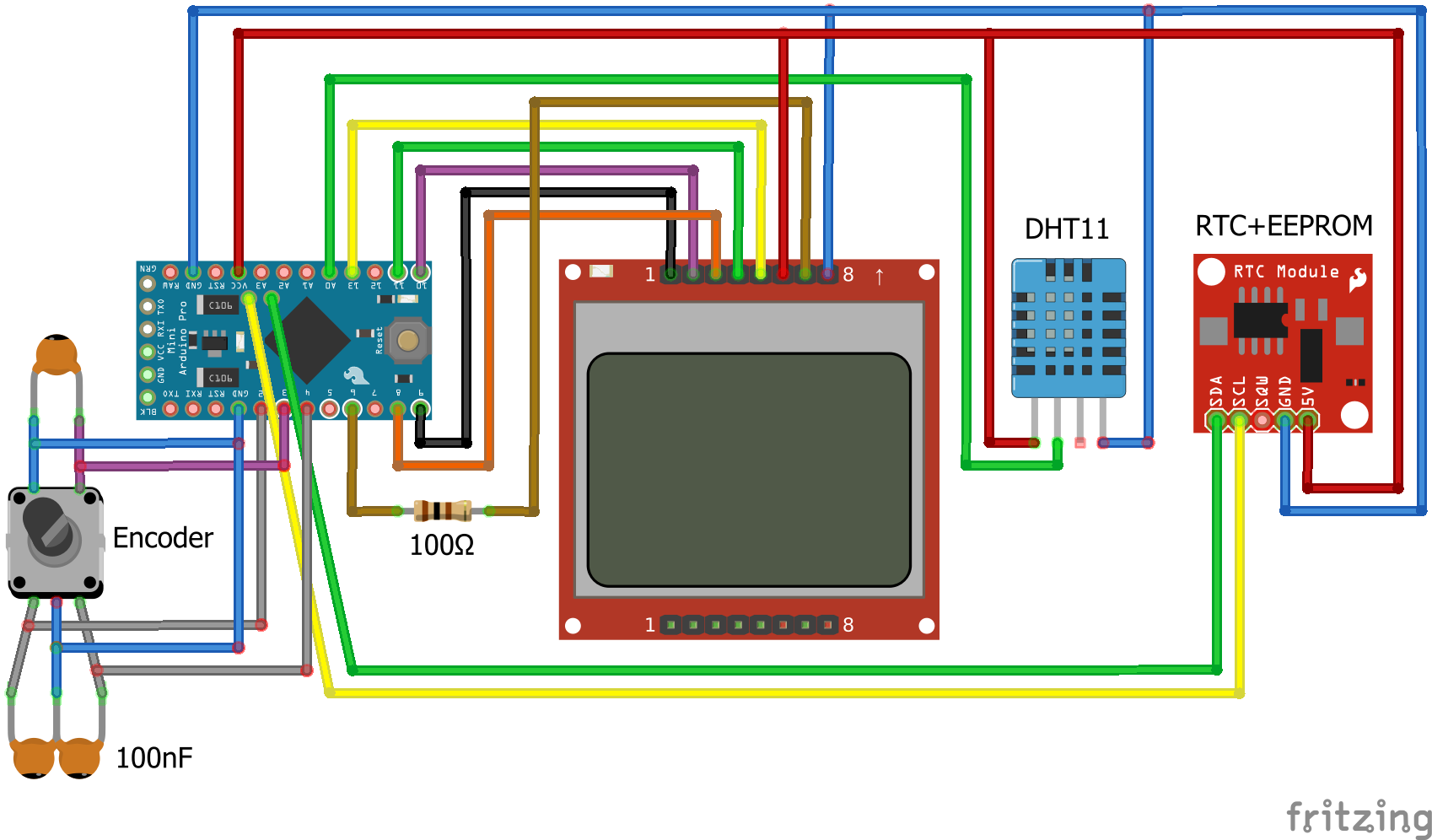
Schematics
The schematics for this project takes a bit of effort. Connect the components as shown in the schematics below.
Schematics
To make the connections easier to follow, a pin map showing how the components are connected is shown in the list below.
To allow for low-level interaction with the EEPROM on the DS3231 RTC, and to use minimal processing resources, we will use a custom library created by cbm80amigato interact with the components. Alongside the libraries, we will also create and use custom fonts which will allow users to view the data in different ways.
Since the libraries we plan to use are not standard libraries and can not be installed with the Arduino IDE, we will add them into the same folder as the code for our project so it can be easily accessed by the code. This can be done by simply copying the library files and pasting them in our project’s sketch folder.
Overall, the sketch contains over 1000 lines of code, as such, it will be impossible to explain it line by line, I will do a brief explanation to cover the basics.
We start the code by including the libraries mentioned above with the fonts we plan to give the users access to. Asides these libraries, we will also use the Nokia 5110 SPI Library and Arduino builtin libraries like; wire.h, EEPROM.h, and the AVR library. The wire.h library is used to enable SPI and I2C communication, the EEPROM library is used to make communication with the EEPROM less tedious and the AVR library is used to implement low power/sleep mode related features.
Next, we declare the pins of the Arduino to which the pins of the components are connected and also declare some of the variables that will be used during the project.
// -------------------------
#define encoderPinA    2
#define encoderPinB    4
#define encoderButton  3
volatile int encoderPos = 0;
#define DHT11_PIN 14
#define BACKLIGHT 6
#define BACKLIGHT_MAX 11  // for always on
#define BACKLIGHT_MIN 1   // below is always off
long menuTime=0;
long logTime=0;
long lightTime=0;
int logInterval = 30;     // in minutes
int backlight = 10;       // in seconds

#define REAL_SLEEP_8S 9100L
Next, we create a struct function to log the data.
struct LogData {
  int hour,minute,second;
  int year,month,day,dayOfWeek;
  int humidity;
  float temperature;
};
To make the code modular, and ensure the void loop() function is not choked with too much code, the project was broken down into a dozen of functions each one to perform a particular task reading the encoder to determine the current screen that should be displayed to reading the DHT to get temperature and information etc. These functions are quite much and it may affect the readability of the tutorial, so you can check them out in the code, which is attached in the file under the download section.
With all the required functions in place, the next line of action is to write the void setup() function. We start by initializing serial communication and also kickstarting communications 0ver I2C by initializing the wire library. We then proceed to initialize the encoder, turn on the backlight of the LCD and get the EEPROMs ready for data exchange.
The loop function starts by checking the battery and issuing a warning if it’s too low, then proceed to get the current date and pull the DHT pin to obtain temperature and humidity data. The temperature and humidity value are then ranked as minimum or maximum in such a way that they replace whatever value is there currently if lower or higher than it is respectively. These values are then displayed in a format that depends on the current screen in view.
To preserve power, a function called power down was implemented. It puts the microcontroller in sleep mode for a few seconds when it is not in use.
The complete code for the project is attached under the download section of the tutorial.
As mentioned during the introduction, the code for this project builds heavily on the code created during the Arduino Nokia 5110 Menu tutorial we published a while back. You can check that out to better understand how the code for this project works.
Demo
Go over the connections once again to ensure everything is properly connected, then connect your Arduino board to the computer and upload the code.
After a while, you should see the screen come up as shown in the image below.
Navigate through the screen, up and down, by turning the rotary encoder in any direction, and select an option by pushing the knob down (click the button on the encoder) to select any of the options. This opens one of the wonderful ways we have created for you to view the data.
Improving the Project
The goal of this project was to show what can be achieved, as such, there was a huge number (maybe too many) of options to show how data can be viewed on the Nokia 5110. You can start improving the project by eliminating some of these options, turning it into a streamlined, useful piece of hardware.
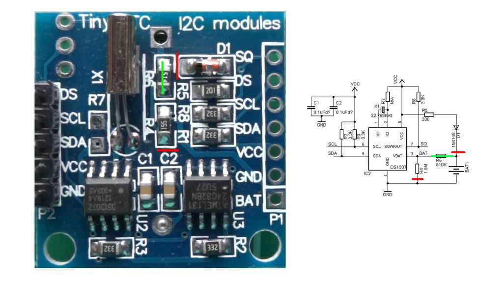
Another thing you can do to improve the project is to reduce power consumption and increase how long the device’s battery lasts. While steps in the right direction have already been taken with the sleep modes incorporated in the code, more can still be done by either using power-efficient components or modifying the current components to remove things wasting power.
For instance, by cutting certain traces (highlighted with red in the image below) on the DS1307, and removing the resistor R6 to be replaced by a solder joining bridging the two points where the resistor was soldered, we will be able to considerably reduce the amount of power consumed by it without affecting performance.
That’s if for today’s tutorial, thanks for reading and following through. Feel free to reach out to me via the comment section if you have questions about the project.
The video demonstration of this tutorial by cbm80amiga can be found on youtube.