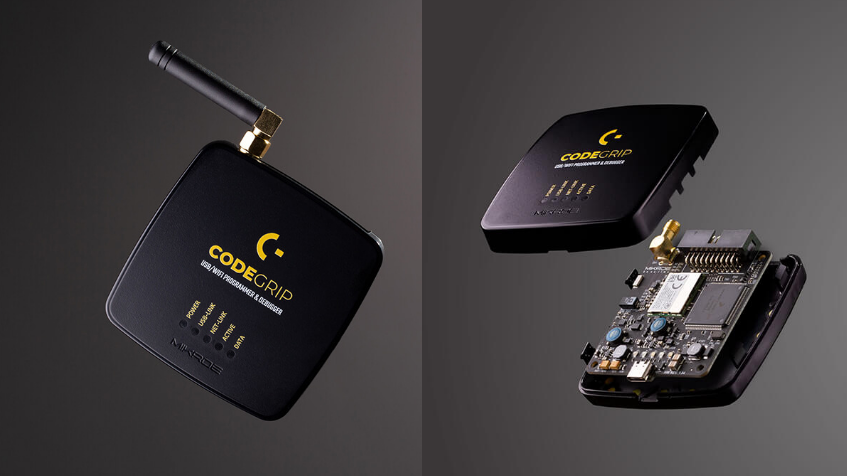
Mikroe known for its array of software and hardware tools for developing embedded systems is offering a universal programmer and debugger for ARM processor that allows programming over USB-C or WiFi. The device is called the CODEGRIP FOR ARM.
CODEGRIP for ARM is a universal programmer and debugger that is built for programming different set of microcontroller devices based on the ARM® Cortex®-M architecture. It supports ARM Cortex M0, M3, M4, and M7. Furthermore, it is capable of working with about 1611 MCUs in the market ranging from STM32, Kinetis, TIVA, CEC, and MSP families of the processor and more MCUs will be added in the future. With it’s carefully built and its aesthetic look, CODEGRIP is a debugger/programmer to have and be absolutely proud of.
CODEGRIP for ARM is a fast USB-C and WiFi programmer and hardware debugger. It supports ARM Cortex M0, M3, M4 and M7 based MCUs.
CODEGRIP for ARM provides extra interfacing options as compared to other programmers designed for ARM with the inclusion of wireless programming and the idea of using USB-C. Mikroe has even claimed it is the “World’s First Debugger Over WiFi,” well not sure if that claim is valid or not since we have seen quite some other WiFi hacks for ARM debuggers. The USB-C connector offers better performance and better use cases, compared to the traditional used USB Type A/B connectors. With the Wireless connectivity, you don’t have to be limited by some physical connection, and this will help speed up troubleshoot and development time.
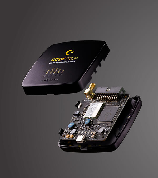
The device is set to be available in two main variants: as a stand-alone device and as an integrated onboard module. Little or no information is provided for the integrated onboard module, and no option to select it during purchase. CODEGRIP can be used with any platform equipped with known JTAG/SWD programming header which can be connected to headers on the CODEGRIP.
Mikroe is also offering a set of different JTAG/SWD programming/debugging header adapters that can be used with various devices to ensure compatibility and is available as an additional purchase option for $9.
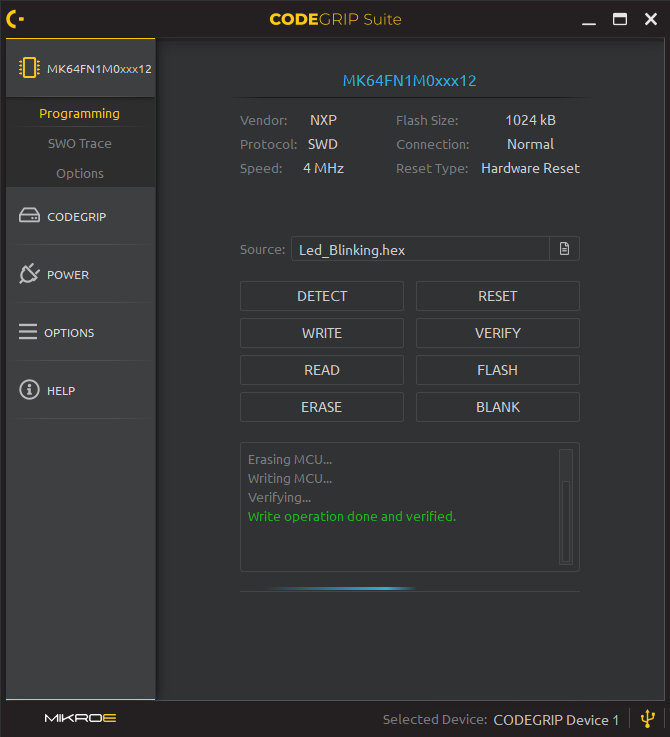
CODEGRIP Suite is a powerful software tool
At the core of the device is the CODEGRIP Suite, a powerful software tool built for managing programming tasks and configuring the CODEGRIP device. The suite can work with multiple CODEGRIPs at once and uses a link structure to avoid ambiguity.
CODEGRIP for ARM is available for $199.00, a price that sits with other similar devices in the market. The package contains:
Flat Cable with 10-pin 0.10″ pitch female connectors
Although CODEGRIP is built with WiFi connectivity, you will have to purchase a separate license to use the WiFi feature which is going to set you back by an extra $100.00. This license is only valid for one use; thus, you can’t use it for more than one CODEGRIP device.
More information about CODEGRIP for ARM is available on the product page, and the suite software is available for download for free.
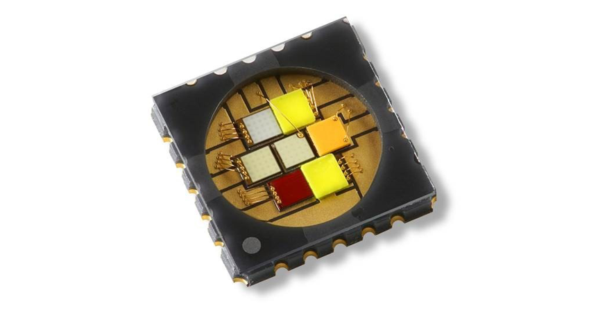
LED Engin LuxiGen™ LZ7 Six-Die LED delivers six colors from a single 7mm2 package. Designed for stage, studio, and special effect lighting, the LuxiGen LZ7 adds PC Phosphor Converted (PC) Amber, Cyan, and PC Lime to the traditional Red, Blue, Green (RGB) LED color set, enabling richer and wider color combinations for more sophisticated color mixing. The compact 3.4mm x 3.4mm Light Emitting Surface (LES) and low-profile design of the surface-mount ceramic package produce an ultra-bright light with narrow beam, as well as high CRI white, all from a single LED emitter.
The LZ7 LED features a patented multi-layer ceramic substrate technology, allowing all six dies to be placed closely together. With an ultra-low thermal resistance of 0.8°C/W, heat is dissipated efficiently from the dies.
The LED Engin LZ7 is offered in a 7mm x 7mm surface-mount ceramic package and pre-mounted on a 7-channel Metal Core Printed Circuit Board (MCPCB).
Features
6-color surface-mount Ceramic LED Package with Integrated Flat Glass Lens
60W max. power dissipation
Red, Green, Blue, PC Amber, Cyan And PC Lime enables richer and wider color combination for more sophisticated color mixing
Compact 3.4mm x 3.4mm Light Emitting Surface (LES) and low-profile package maximize coupling efficiency into secondary optics
Thermal Resistance of 0.8°C/W
Electrically Neutral Thermal Path
JEDEC Level 1 for Moisture Sensitivity Level
7.0mm x 7.0mm Emitter Footprint
Lead (Pb) Free and RoHS Compliant
Specifications
DC Forward Current Per Die (IF(MAX)):
Red: 2500mA
Green: 3000mA
Blue: 3000mA
PC Amber: 1500mA
Cyan: 1000mA
PC Lime: 2500mA
Power Dissipation (Pd): 60W
Luminous Flux @ IF = 1000mA (ΦV):
Red: 95lm
Green: 180lm
Blue: 42lm (1.2W)
PC Amber: 140lm
Cyan: 135lm
PC Lime: 620lm
Viewing Angle: 114°
Note: This product emits Blue light, which can be hazardous depending on total system configuration (including, but not limited to optics, drive current and temperature). Do not stare directly into the beam and observe safety precaution given in IEC 62471 when operating this product.
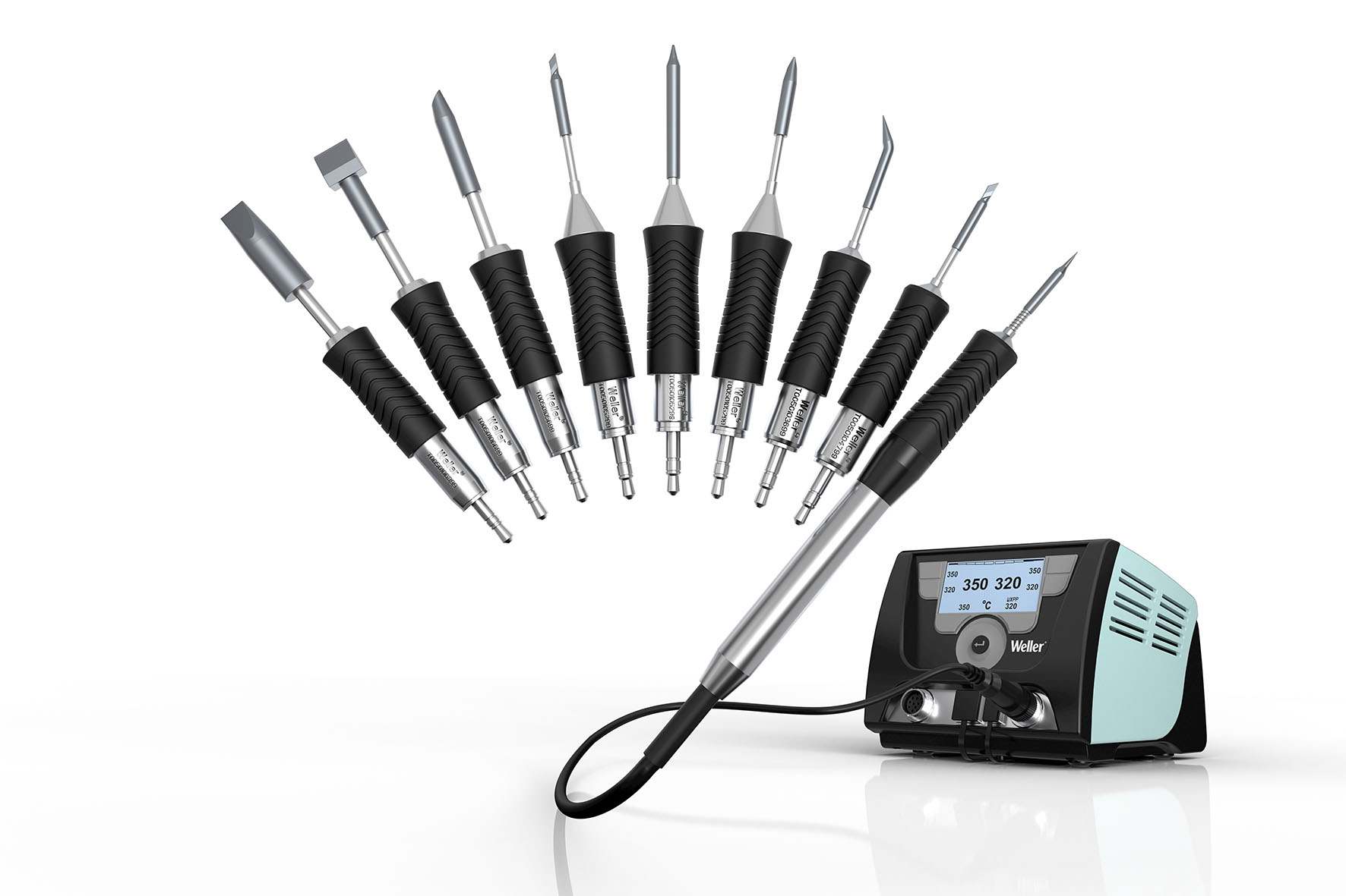
Weller Tools, the world’s No.1 brand in hand soldering solutions, expands its Active RT soldering tip program. The expanded tip series offers the highest precision, while maximizing performance and power. The tips work exclusively with the high performance WX platform of soldering stations.
Widest range of high-end soldering tips
Whether in the electronics field, medical technology or aerospace field, the industry is moving faster and the components are steadily becoming smaller, more complex and more powerful.
The soldering industry is no different and in order to meet these increasing demands, Weller is expanding its existing Active RT soldering tip series. Weller has and will continue to offer the widest range of these high-end soldering tips – all linked to one single soldering station from the WX series. “As always, Weller makes No Compromise: we’re offering maximum performance, power and precision with our new RT Lines of tips. They also provide maximum protection to the PCBs and the components you are soldering, improving yield and ultimately reducing cost”, says Philippe Buidin, VP Marketing, Weller & General Manager, Weller Tools GmbH.
IPC industry standard
The new Active RT soldering tips comply fully with IPC industry standards. The MS versions are also MIL-SPEC compliant and therefore protect both the printed circuit board and component. This not only achieves the best results, but successfully manages to keep running costs as low as possible. The boomerang handle design allows for precise handling while providing an ergonomic and secure grip.
The patented tip/handle unit enables speedy, hassle-free toolless tip change. The extended RT series with the three sub-series RT Pico, RT Micro and RT Ultra covers a wide range of point sizes and geometries for almost every soldering application allowing precision work from the smallest micro range components to robust applications with maximum energy requirements.
RT Pico soldering tips
The new Active RT Pico soldering tips deliver pinpoint performance and maximum precision for micro-soldering applications – even with the smallest micro components that are barely visible to the eye, ranging from 0402 to 01005 in size. The short distance between the soldering tip and handle allows for extremely precise work and maximum control. In this way, damage to the highly sensitive micro components can be prevented reducing the number of expensive rejects.
RT Micro soldering tips
The proven Active RT Micro soldering tip range has been bolstered by new tip sizes and geometries, offering an even broader range of applications as well as extremely fast heat-up and recovery times.
RT Ultra soldering tips
The new Active RT Ultra tips designed for rugged soldering applications meet maximum energy requirements with an innovative Thermal Core heating element. Therefore an individually required energy supply and constant temperature can be guaranteed at the contact point of the soldered surface.
All new Active soldering tips also impress with:
intelligent soldering iron technology, including motion sensor
reduced risk of burns when changing soldering tips
digital data storage in the intelligent soldering tool and in the soldering station
Weller Genuine label
Active RT soldering tips carry the Weller Genuine label. Genuine Weller tips protect the soldering iron from irreparable damage. Weller tips are designed for excellent heat transfer to deliver ideal soldering joints while ensuring optimal and consistent performance which leads to cost savings.
New soldering tip-finder
The extended Active RT soldering tips underlines Weller’s holistic, innovative approach by providing a consistent solution for all high-end applications in combination with five different WX soldering irons and WX soldering stations. The new soldering tip-finder on weller-tools.com/nocompromise can be used to select the best tip for the respective soldering task without compromises. It has never been easier or better to deliver maximum precision, performance with optimum energy at the soldering point.
IoT application development SensiBLE 2.0 by SensiEDGE simplifies cloud connectivity, shortens time to market and accelerate Delivery of Industrialized IoT solution
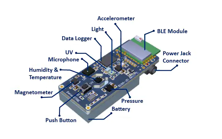
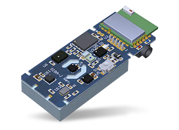
Introducing SensiBLE 2.0, a new portable IoT module in a small form factor (17 x 40mm) powered by a rechargeable Li-Ion battery. Packed with a variety of sensors such as ambient light sensor, UV sensor, pressure sensor, relative humidity sensor, as well as a microphone, SensiBLE 2.0 is a true IoT application accelerator. It features an accelerometer and magnetometer so the device can be used as a digital compass, pedometer or to measure vibration levels.
SensiBLE 2.0 runs on the all-in-one Bluetooth 4.2 module SPBTLE-1S from STMicroelectronics. This is a certified module that includes the BLE v4.2 stack and the low-power ARM® Cortex®-M0 32-bit core. It has been designed to leverage the BlueNRG-1 integrated DC-DC step-down converter in order to achieve low power consumption in active mode. The module runs at 32MHz, which is more than enough for most applications. In addition, the module has 160 KB of flash and 24 KB of embedded RAM with data retention.
SensiBLE 2.0 is fully compatible with STBLESensor application (available for Android and iOS). This program makes it easy to read values and send them to Cloud. Also available to designers is SensiBleWindows, a unique SensiEDGE application for Windows. The source codes and SDK of both programs can be found on the GitHub, and its license allows designers to edit their source codes based on their individual requirements.
ARM® 32-bit Cortex®-M0 CPU High performance, ultra-low power processor
Data Logger: 4Mbit SPI_Flash
Serial Flash: AT25XE041B-MHN-T
Sensors
Accelerometer: LIS2DW12
Magnetic sensor: LIS2MDL
Pressure sensor: LPS25H
Relative humidity & temperature: HTS221
Digital MEMS Microphone: MP34DT05-A
Light Sensor: APDS-9250
UV Sensor: VEML6075
User Interface
I/O Expander: FXL6408
RG LED: LTST-C195KGJRKT
User Button: KMR221NG
Power Interface
Rechargeable Battery
Micro – USB on Debugger Board
External Power: 4.25V <Vin <6.5V
SensiBLE 2.0 is an industrial-grade customizable solution for design engineers looking to design IoT products without getting involved in either hardware development or production logistics. A key benefit of SensiBLE2.0 is that it allows developers to focus on their own applications, domain expertise and core competencies, rather than the underlying hardware platform or production logistics when creating products for the IoT.
The SensiBLE 2.0 software code is available online and it can be easily customized. For example, it is possible to configure an external FLASH memory located on the board to store sensor measures if a BLE connection is lost; when the connection is restored, all data received during this downtime can be transferred.
FM radio transmitters and receivers are one of the projects that fascinated a lot of people and drove them to become makers. The lure of being able to deploy your own radio station, or build your own surveillance(-like) devices was what encouraged most of us to build our first fm transmitter or receiver. Nowadays, microcontrollers help simplify and add a lot of functions to analog projects that’s why for today’s tutorial, we will look on how you can build an Arduino based FM radio receiver using the TEA5767 FM radio and an Arduino Nano.
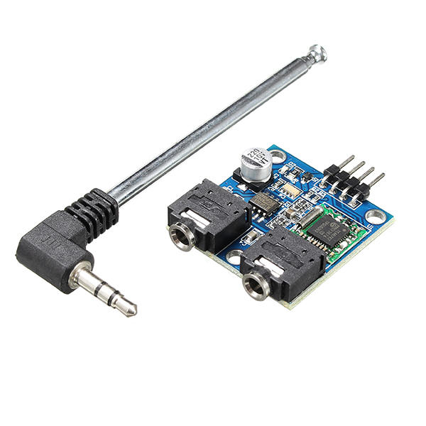
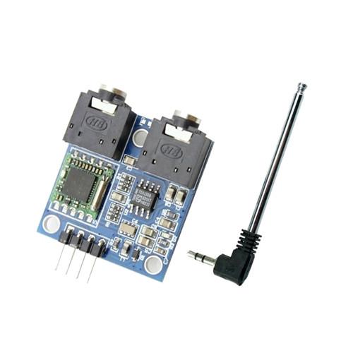
TEA5767 FM Radio Receiver Module
At the heart of today’s project is the cheap TEA5767 FM radio module. This module comes with all the components required to build a FM radio receiver, all on board. The module is based on the TEA5767GH which is a single-chip, electronically tuned, FM stereo radio for low-voltage applications with fully integrated Intermediate Frequency (IF) selectivity and demodulation. Through an I2C interface, the module can be connected to a microcontroller to digitally control its tuning frequency and other characteristics, giving room for opportunities to digitize some of its operations. It comprises of two headphone jacks, one of which is for connection to an headphone/speaker while the other is for connection to the antenna which usually comes with the module.
Some of the features of the TEA5767 chip are outlined below:
High sensitivity due to integrated low-noise RF input amplifier
FM mixer for conversion to IF of the US/Europe (87.5 MHz to 108 MHz) and Japanese (76 MHz to 91 MHz) FM band
Preset tuning to receive Japanese TV audio up to 108 MHz
RF Automatic Gain Control (AGC) circuit
LC tuner oscillator operating with low cost fixed chip inductors
FM IF selectivity performed internally
No external discriminator needed due to fully integrated FM demodulator
Crystal reference frequency oscillator; the oscillator operates with a 32.768 kHz clock crystal or with a 13 MHz crystal and with an externally applied 6.5 MHz reference frequency
Phase-locked loop (PLL) synthesizer tuning system
I 2C-bus and 3-wire bus, selectable via pin BUSMODE
7-bit IF counter output via the bus
4-bit level information output via the bus
Soft mute(Can be switched off via Bus)
Signal dependent mono to stereo blend
Stereo Noise Cancelling (SNC)(Can be switched off via Bus)
Signal dependent High Cut Control (HCC) (can be switched off Via Bus)
Adjustment-free stereo decoder
Autonomous search tuning function
Standby mode
Two software programmable ports
Bus enable line to switch the bus input and output lines into 3-state mode
More info on the chip can be found in its datasheet.
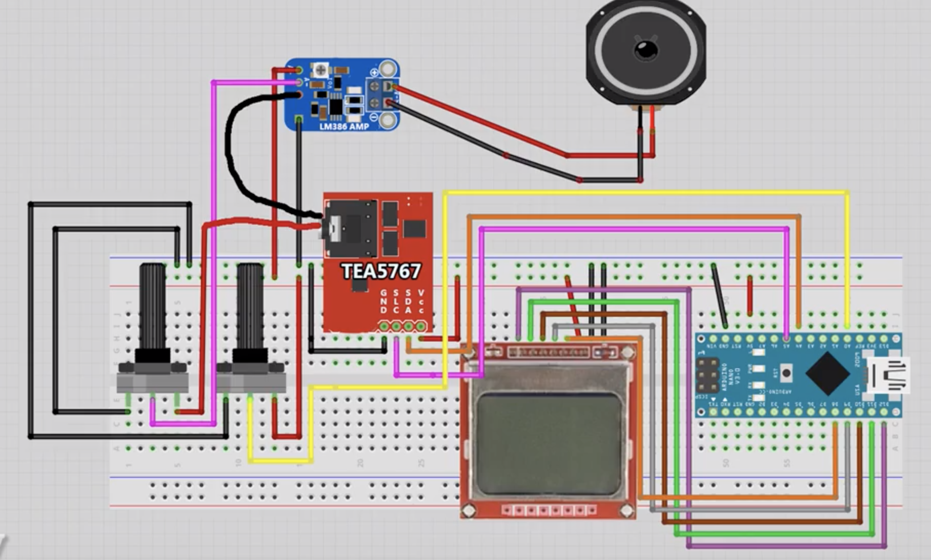
For this project, we will connect the FM module to Arduino nano, so we will be able to set its tune frequency, display its signal strength, current frequency, stereo mode and other. The Nokia 5110 LCD will be used as the system’s display, providing visual feedback to the user while potentiometers are used to set the frequency and volume of the radio receiver. Turning the knobs in one direction will increase the volume or increase the frequency (depending on the particular knob being turned) and vice versa.
To test our radio receiver when the built is finished, we will use a small inexpensive FM radio transmitter (pictured above) which can be connected to our mobile phone to broadcast sound coming from it. Be sure to only use this within the limit defined for unlicensed broadcasting in your country, state or region.
Lets jump in
Required Components
We will need the following parts to build this project;
As usual, the exact model of these components that will be used for this tutorial can be bought via the links attached. The total cost of the project is around 15$ and could be lesser if you already have some of the components at home. The power bank is only used to make it easy to use the radio without being it tethered to a PC.
Schematics
The schematics is a bit straight forward. The FM radio is connected to the Arduino via I2C while the Nokia 5110 is connected the same way as several of our past tutorials involving it. The only tricky part of the schematics is the connection of an external amplifier to the module. The inbuilt output amplifier for the module was designed to work with headphones, as such, the audio signal quality is poor when a speaker is connected to it. To amplify the sound, the module will be connected to an external amplifier.
Connect the components as shown in the schematics below;
Schematics
As usual, a pin to pin description of the connection between the components is shown below;
A lot was done using the Nokia 5110 LCD display in this tutorial, as such, it might be beneficial to check out some of our past tutorials, especially the tutorial on displaying custom graphics on the Nokia 5110 display.
Code
With the components all connected, we can now proceed to write the code for the project. The sketch for today’s project relies heavily on two libraries; the LCD5110_Graph library and the TEA5767N library. The LCD5110_graph library facilitates interaction with the Nokia5110 LCD display, making it easy to display graphics and text using functions, while the TEA5767, facilitates the interaction between the microcontroller and the FM Radio module.
To do a quick run through the code and provide an explanation to some of the concepts, we start the sketch as usual, by including the libraries that will be used for the project.
   /////////////////////////////////////////////////////////////////
   //                 Arduino FM Radio Project                    //
  //       Get the latest version of the code here:              //
 //     📥 http://educ8s.tv/arduino-fm-radio-project            //
/////////////////////////////////////////////////////////////////

#include <TEA5767N.h>  //https://github.com/mroger/TEA5767
#include <LCD5110_Graph.h> //http://www.rinkydinkelectronics.com/library.php?id=48
Next, we create an instance of the LCD graph library named LCD, with the pins of the Arduino to which the LCD is connected as arguments. We also create an instance of the TEA5767 library named radio.
LCD5110 lcd(8,9,10,12,11);
TEA5767N radio = TEA5767N();
Next, we create variables to hold the fonts that we will use on the LCD and also create variables to hold the icons that we will use to show the volume level. The byte array to hold all of these icons is going to be placed in the same folder as the code for the project so they can be easily referenced.
Next, we declare the analog pin to which the potentiometer that controls the frequency is connected and also create variable names to hold the values of the raw value of frequency (int), current frequency, previous frequency alongside a variable to store the signal strength of the FM signal.
int analogPin = 0;
int val = 0;
int frequencyInt = 0;
float frequency = 0;
float previousFrequency = 0;
int signalStrength = 0;
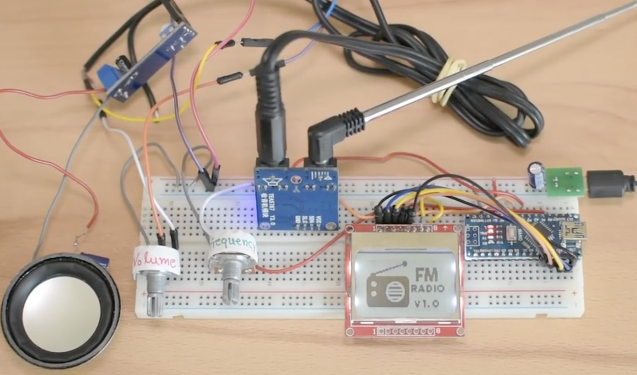
With this done, we proceed to write the void setup() function. We start the function by initializing the radio module, setting the mono reception and instructing it to cancel stereo noise. Next, we initialize the display using the initScreen() function and display the splash screen. The splash screen for this project was developed using photoshop and converted to a byte array using bitmap converter. You can check out one of our past tutorials on displaying custom graphics with the Nokia 5110 display to better understand how that works.
Next, is the void loop() function. We read the values from the potentiometer that controls the frequency every few milliseconds and map it to our frequency value.
for(int i;i<30;i++)
{
   val = val + analogRead(analogPin);
   delay(1);
}

val = val/30;
frequencyInt = map(val, 2, 1014, 8700, 10700); //Analog value to frequency from 87.0 MHz to 107.00 MHz
float frequency = frequencyInt/100.0f;
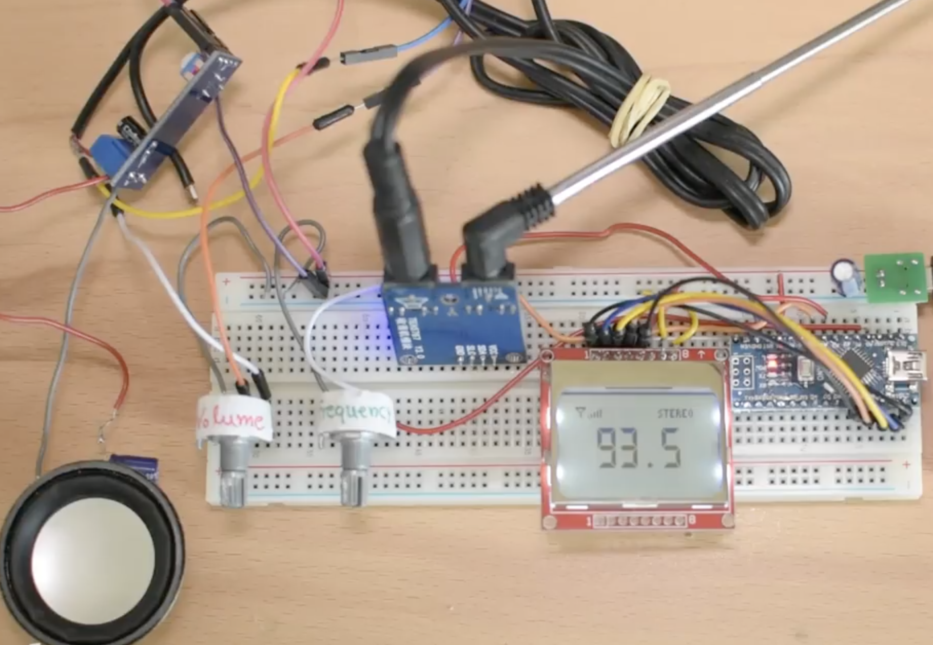
To prevent noise and achieve a stable tune, we only change the frequency of the radio module when there is a considerable change between the last frequency and the current value set by the potentiometer.If a significant difference exists, we then use the radio.selectFrequency() function to tune the radio to that frequency. After this, we obtain the signal strength at that frequency and display it on the LCD using the PrintSignalStrength() function, followed by the display of the stereo state and the display of the frequency on the LCD. The current frequency is then mapped to the previous frequency, awaiting the next time, the frequency is changed.
Go over the connections once again to ensure everything is as it should be, especially the connection between the external amplifier and the speaker. With that done, connect the Arduino to your computer and upload the code. Ensure all the libraries have been installed to prevent errors. With the code upload successful, after a couple of seconds, you should see the splash screen come up as shown in the image below.
Demo
This will then be followed by the main window which displays the current frequency to which the radio is tuned.
Demo
Turn up the volume and tune the radio to any of your local stations, you should now be able to hear the radio. Another way to test your receiver is to use an inexpensive radio transmitter which can be connected to your mobile phone and tune the radio to its frequency. However, be sure to ensure you are within the provisions of the law of where you are, this last approach may be classified as unlicensed broadcasting in some places.
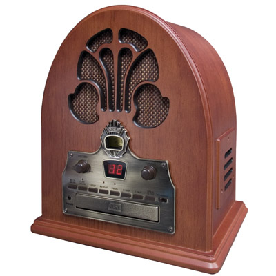
That’s it for this tutorial guys; your own personal FM Radio Receiver. While this system is characterized by the poor audio output, with the use of a better amplifier to improve the sound, and a 3D printed or CNC machined enclosure, it could be transformed into a fantastic retro styled FM radio like the one in the image below. Feel free to reach me via the comment section for answers to any question you might have about this project. Look forward to seeing your Retro FM radios.
Retro Style FM Radio
The video version of this tutorial is available on youtube.
It’s one thing to have an idea (especially a hardware-based idea) and it’s another thing to bring it to life. Rapid Prototyping using tools like 3D Printer has opened a lot of opportunities for the everyday makers, hardware enthusiasts, and hackers. For the person looking to build that next cool thing, maybe a PoV (Persistence of Vision) display, and some flying racing car, one thing is sure you are going to get your hands dirty by making some sort of electronics board to control it all.
image: www.ssalewski.de
At the heart of every electronic board is the PCB design; it puts everything together so it could be produced. It’s one thing to know how to develop an electronic circuit, but it’s another thing to get PCB the way you want. EDA software like Altium, OrCAD, KiCad, Eagle, and others provides the opportunity to convert your schematic to a PCB design to finalize your project, but you will most likely won’t get all the PCB footprints needed for each component of your circuit. One solution is to start creating your own footprint or library for that component which will require digesting the datasheet properly; this process could be time-consuming and frustrating sometimes when you are using the wrong platform or working with a large number of pins.
Fortunately, there are other ways around this. There exist many online resources contributed by experienced engineers and hackers that have created layouts, footprints, libraries that could be used by anyone for free or at a price. These platforms have reduced the workload of the PCB design engineers and makers. Some well known platforms to source for PCB footprints are listed below:
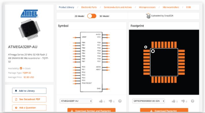
As they say, you can’t call yourself a professional PCB or Hardware engineer without having to use SnapEDA before. At SnapEDA, you can search for the schematic symbols and PCB footprints of millions of major components. SnapEDA’s vision is to eradicate the need of creating your own library or footprint ever again, with access to millions of components, hardly will you not find what you are seeking. Furthermore, SnapEDA also offers to deliver a footprint for a part not generally available for you within 24 hours! They support footprints and models for the most common CAD software like Altium, Eagle, KiCAD, OrCAD, PADs, PCB123, and Pulsonix.
Just like SnapEDA, Ultra Librarian it’s also a rich platform to find most component footprint you are looking for. They offer both 2D, 3D, layout, the footprint of most components and even supports a lot of CAD software. They are available to download for free. Both platforms, Ultra Librarian and SnapEDA provide purchasing options for the end-user. They list several stores where you can purchase the components you are looking for and offer you the full package.
For the KiCad hardcore fans, this is for you. KiCad is known for its opensource software also provides official libraries that are readily available for download on their website. They include schematic symbols, PCB footprints, and comes complete with 3D modeling data to complement their 3DViewer tool, which enables you to inspect your design more in detail with an interactive 3D view. The libraries are available on GitHub for download and even collaboration.
Popular Electronics Stores
Arduino became famous thanks to the community support from popular online retail stores like Sparkfun, Adafruit, Seedstudio, Digikey, and others. Not only do these guys provide sales of electronic components, but they also offer powerful community support for the hardware ecosystem, and most of Eagle’s success can be attributed to them. Sparkfun, Adafruit, Element14 have produced opensource projects to the community while also releasing the source files (schematic, PCB, 3D models) to the public. Most of the footprints and source files are only available in Eagle though.
SparkFun and Adafruit, well-known websites catering to the maker community, provide Eagle with source files (schematic, PCB, library)
Sparkfun provides a wealth of resources. Some of the resources from Sparkfun can be sourced from Sparkfun Eagle, and it’s Github repository of Eagle-based footprints here.
Seeed Studio has its very own Open Parts Library (OPL) which is a collection of over 10,000 commonly used components sourced explicitly for the Seeed Fusion PCBA Service. Seeed is building the component libraries for KiCad and Eagle. For KiCad, the library can be downloaded from the GitHub page, whereas the Eagle version can be downloaded and updated from within Eagle, making it much more convenient for designers.
10. Eagle – Autodesk Eagle provides its own arsenal of libraries contributed by experts over the years which are available here.
These conclude some of the top 10 websites and platforms to get those tricky footprints and models to use for your next project. Have a suggestion of some sites that can also be added? Please include in comments below. Stay tuned for my next post on some of the top websites to get project inspiration to work on, for the time being, get some inspiration from the Elabs project section.
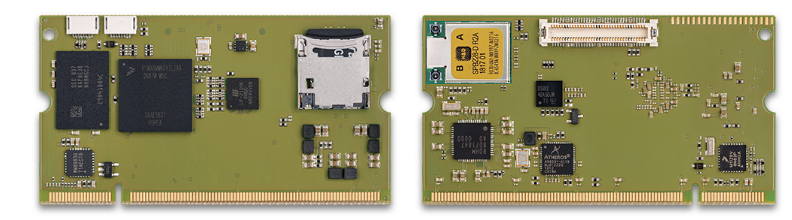
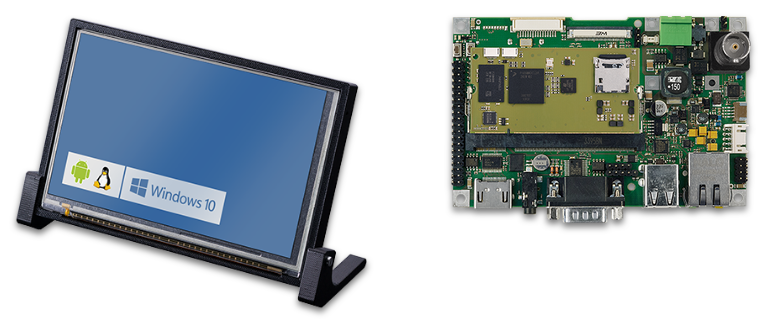
The new Trizeps VIII uses the i.MX 8M processor from the NXP i.MX8 series. The CPU Module provides the high performance demands of current video, voice, and audio processing, either for industrial or home automation, streaming audio applications, or for modern imaging devices.
Available with Linux and Android operating systems, Windows 10 IoT Core is announced.
NXPTM i.MX 8M ARM® Quad-/Dual-Core Cortex A53 CPU up to 1.5 GHz, additional Cortex M4
Configurable FPGA, e.g. with MIPI to RGB converter
Additional NXPTM Kinetis V ARM® Cortex M0+ MCU with e.g. CAN, ADC, SPI, I2C interfaces
Up to 4 GByte LPDDR4-3200 RAM, 32Bit
1 GBit Ethernet, USB 3.0
Onboard WLAN/Bluetooth module (optional)
LVDS (Single or Dual) Transceiver
Trizeps SODIMM-200 compatible, compact and scalable
Features:
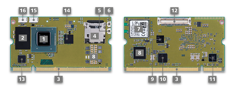
1 NXP i.MX 8M Arm Cortex A53 CPU up to 1.5 GHz (Quad-, Dual-Core), additional Cortex M4 – 2 LPDDR4-3200 RAM (32 Bit, up to 4 GByte) – 3 SODIMM 200 Connector, Interfaces: UART (4x), SPI, SDIO, QSPI, I2C (3x), GPIO, PWM, USB 3.0 (2x), Headphone (stereo), Line-In (stereo), Microphone, Speaker, SPDIF In/Out, Serial Multichannel Audio, PCM, PCIe, FPGA configurable pins (e.g. display RGB16/18/24, SPI/UART/GPIO, parallel camera), Kinetis MCU Pins (e.g. CAN, ADC 16 bit, UART, SPI), Ethernet (1 Gbit, 100/10 Mbit), +3V3 power supply – 4 Socket for µSD cards (4 Bit, lockable, optional) or eMMC (8 Bit, Standard) – 5 WLAN and Bluetooth UFL Coax connector (2,4 GHz, 5 GHz) – 6 WLAN UFL Coax connector (2,4 GHz, 5GHz) – 7 WLAN-Bluetooth Module (optional): 802.11 a/b/g/n/ac 2×2 MU-MIMO / Bluetooth 4.2, 5.0 – 8 Power Management IC (PMIC) – 9 Single or Dual LVDS Transceiver – 10 1 Gbit Ethernet Phy – 11 NXP Kinetis MCU, Cortex M0+ – 12 High-Speed board-to-board connector, Interfaces: HDMI, Mipi DSI (4 channel), Single or Dual LVDS, 2x Mipi CSI (4 channel), Ethernet SIOP – 13 HiFi Audio Codec – 14 FPGA up to 4300 LUTs – 15 JTAG (i.MX 8M CPU) – 16 JTAG (FPGA and MCU)
Constantly high quality through multi-stage test of each individual CPU module
To ensure a constantly high quality, each individual CPU module is passed through a multi-stage test. The test result covers 100% of all interfaces.
AOI/MOI: Multiple automatic and manual optical control of each CPU module during the production.
JTAG/Boundary Scan Test: JTAG/Boundary Scan Test: The signal of each pin which is accessible via the JTAG chain is checked for connection, shorts, missing pull-up/down resistors. The DDR Ram is tested for row/column pin assignment.
Functional tests of high-speed and analog interfaces (Ethernet, display, USB, audio, etc.) which are not testable via JTAG
SODIMM Standard
The Trizeps VIII includes the Keith & Koep SODIMM 200 Standard, the world‘s longest existing SODIMM standard. Like no other module standard, the SODIMM 200 ensures the pin compatibility of the Trizeps modules. The main difference of the Trizeps VIII Mini is the missing address/data bus, which is no longer supported by the i.MX 8M CPU. The pins, which are no longer needed for this function, are used for GBit Ethernet and USB 3.0 signals. Trizeps VIII and Trizeps VIII Mini are mostly pin compatible.
i.MX 8M / i.MX 8M Mini Evaluation Kit with 7.0″ TFT Display
Further information
No pricing or availability information was provided for the Trizeps VIII and Trizeps VIII Mini modules or the pConXS Eval-Kit. More information may be found at Keith & Koep’s Trizeps VIII, Trizeps VIII Mini, and pConXS Eval-Kit product pages.
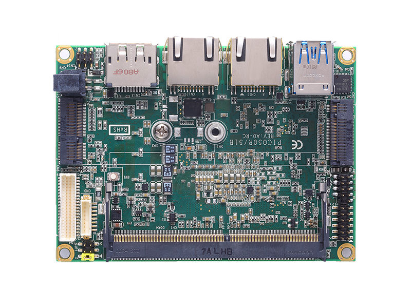
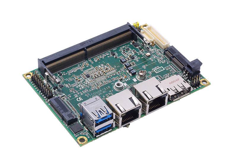
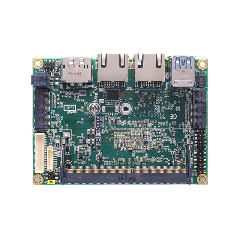
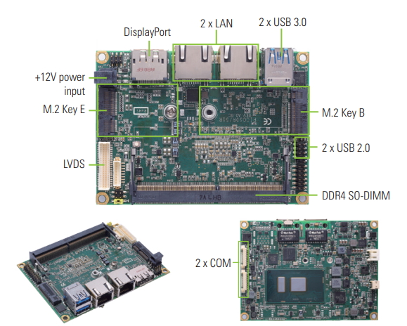
Axiomtek – a world-renowned leader relentlessly devoted in the research, development and manufacture of series of innovative and reliable industrial computer products of high efficiency – is introducing the PICO51R, an ultra-compact 2.5-inch pico-ITX motherboard powered by the 7th generation Intel® Core™ i7/i5/i3 or Celeron® processor (code name: Kaby Lake). With the onboard CPU attached on the rear side of the board, the PICO51R can aid the heat-extraction process to make fanless design possible and make system integration fast. The pico-ITX embedded board also provides practical expansion interfaces within its limited dimensions including one M.2 Key E slot for wireless modules and one M.2 key B slot for storage cards. The compact-sized rugged PICO51R is the perfect platform for industrial automation applications requiring a small form factor to fit in space-limited environments.
“Axiomtek’s PICO51R with high flexibility and expansion possibilities offers diversity and flexibility for system integration. This powerful 2.5-inch Pico-ITX embedded motherboard is designed for minimum maintenance and maximum ruggedness,” said Michelle Mi, a product manager of ECSE Division at Axiomtek. “In addition to two USB 3.0 (USB 3.1 Gen1) ports in support of industrial cameras for machine vision applications, the PICO51R also comes with an M.2 Key E slot for wireless communication capabilities and two Gigabit Ethernet ports for mass data transmission or LAN port teaming functions.”
The Intel® Core™-based PICO51R supports one 260-pin DDR4-2133 SO-DIMM for up to 16GB of system memory. Moreover, the pico-ITX single board computer utilizes Intel® HD graphics engine to bring a true high definition visual experience with dual display configurations through DisplayPort and 18/24-bit single/dual channel LVDS. In addition, this industrial motherboard can withstand a wide operating temperature range from -20°C to +60°C (-4°F to 140°F) for use in rugged and harsh environments.
The PICO51R adopts a rich array of I/O interfaces including two USB 3.0 ports, two USB 2.0 ports, two Gigabit Ethernet ports with Intel® Ethernet Connection I219-LM and Intel® Ethernet Controller I211-AT, two RS-232/422/485 ports, one I2C port and 4-bit DIO port. The board requires only +12V DC power supply input. To ensure reliable operation, it supports a watchdog timer to detect and recover from computer malfunctions and supports hardware monitoring features to monitor temperature, voltage, fan speed, and more. Furthermore, it supports Intel® Active Management Technology 11 (Intel® AMT 11) for remote management.
Two USB 3.0, two USB 2.0 and two COM (RS-232/422/485) ports
One M.2 Key E
One M.2 Key B
Supports Intel® Active Management Technology 11 (Intel® AMT 11)
Features +12V DC power supply input with AT Auto Power On
Extended operating temperature ranging from -20°C to +60°C
Axiomtek’s PICO51R is available now. For more product information or customization services, please visit our global website at www.axiomtek.com or contact one of our sales representatives at info@axiomtek.com.tw.
Among the key subjects on PCB Gold Finger include:
Gold Fingers PCBs: This section provides a brief overview of the definition of the gold fingerprinted circuit board and the reasons why the gold finger circuit board needs to be gold plated. It also introduces the two main gold plating types of the gold finger: Electroless Nickel Immersion Gold (ENIG), Hard plated Gold over Nickel.
How Do You Make Gold Finger PCBs?: This section details the three aspects of making gold finger PCB : 2.1 Common gold plating involved steps: This section focuses on the three stages of Common gold plating. 2.2 Making other types of gold finger PCBs: This section mainly introduces two favorite kinds of PCB gold fingers: Unequally Sized Gold Finger PCBs, Making Segmented Gold Fingers, and the steps to make a segmented gold finger PCB. 2.3 Limitations of Gold Finger PCB Technology: This section describes the limitations of Goldfinger PCB technology in four aspects.
Applications & Limitations of Gold Finger PCBs: This section mainly describes the technical implementation, and commercial use of the Golden Fingerprinted circuit board.
Regulations, Guidelines & Standards: This section details the rules, guidelines, and standards for Gold Fingers PCBs.
Besides, The focus of this article is hope that your printed circuit board production is fully compliant with IPC standards, in an incredible bargain and timely delivery, please feel free to make an online PCB quote with us.
About WellPCB
WellPCB is focusing on PCB Prototype and PCB Assembly Turnkey Services. All PCBs products are compliant to ISO, UL, IPC Standard.
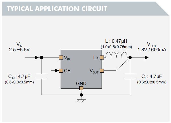
Torex Semiconductor Ltd. have developed 4 MHz product of XC9281 / XC9282 series which released in November 2018.
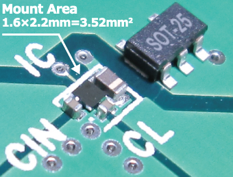
The XC9281 / XC9282 series are 600 mA synchronous rectification DC/DC converters adopting HiSAT-COT (*) control. By adding an oscillation frequency of 4 MHz, high efficiency can be realized while maintaining the mounting area as compared with the oscillation frequency of 6 MHz of the conventional XC9281 / XC9282 series. (Figure 1)
With an oscillation frequency of 4 MHz, 1uH coil with a size of 1.0 x 0.5mm can be used. A 0.6 x 0.3mm ceramic capacitor can be used for the input capacitance (CIN) and the output capacitance (CL), realizing that the mounting area including peripheral components can be reduced to 3.52 mm2.
Because of these features, XC9281 / XC9282 series are ideal for equipment requiring miniaturization and low profile mounting area, and battery-powered equipment such as mobile.
Moreover, the high-speed transient response technology of the HiSAT-COT control makes it possible to minimize the fluctuation of the output voltage for a load transient condition. This feature is optimal for applications requiring a fast response and output voltage stability for an instantaneous load fluctuation like FPGA.
(*)HiSAT-COT is a proprietary high-speed transient response technology which Torex developed and the DC / DC converters with HiSAT-COT technology are ideal for LSI’s that require high precision and high stability power supply voltage.
Torex will continue to swiftly develop products that meet market needs and contribute to a richer and more abundant society.