UP Core Plus – Power UP Your Project with UP Core Plus Modular Boards

AAEON, an award winning developer of Edge AI Computing solutions, announces the 2nd Generation of UP modular boards, the UP Core Plus maker board along with the Net Plus and Vision Plus X docking boards. Together these board kits provide developers and easy way to build a system designed for the needs of their project, whether it’s a compact networking device, or a powerful AI Edge system.

The UP Core Plus is the 2nd Generation of the UP modular maker board from AAEON. Featuring Intel Apollo Lake processors, the UP Core Plus offers a great leap in performance over the previous generation. The board can be configured with up to 8 GB of onboard memory, and up to 128 GB onboard eMMC storage. The UP Core Plus also features USB 3.0, DP, and USB OTG connections, as well as support for wireless and Bluetooth connectivity. The UP Core Plus also supports up to four PCI express lanes thanks to the Apollo Lake processors.

While the UP Core Plus has fewer I/O ports than the UP Squared, it offers unmatched flexibility thanks to its two 100-pin connectors. With these connectors, users can add-on docking boards that help tailor the board to their applications. AAEON currently offers two boards as part of the UP Core Plus family, the Net Plus and UP Vision Plus X.

The Net Plus docking board expands the I/O support of the UP Core Plus system, with four Intel i211 Gigabit LAN ports, or optional Intel i210 with Time-Sensitive Network (TSN) support. It also features a SATA port for hard drive support, as well as an mPCIe slot which supports a wide range of Mini-Card solutions, including 4G, WiFi, and more. The Net Plus is perfect for developers looking to build a compact network device, or to connect multiple network devices to the system.

The Vision Plus X board brings the power of AI@Edge to the UP Core Plus. Featuring three Intel Movidius Myriad X VPUs, the Vision Plus X offers a high-performance solution to powering AI applications. With a built in mPCIe slot, developers can push the count up to four Intel Myriad X VPUs with the addition of the AI Core X module. The Vision Plus X is perfect for bringing to life AI Edge applications such as facial recognition and smart retail.

The UP Core Plus from AAEON offers developers unmatched flexibility to power their projects. Users can use the UP Core Plus board as a standalone system by itself, or expand with the Net Plus or Vision Plus X boards. AAEON also offers a carrier board design guide available through the UP Community, allowing users to build their own custom board configurations and layouts. The 2nd Generation modular board, UP Core Plus from AAEON, is built to power up your project.

Real-time clock for wearables draws under 180nA

More than 35 percent smaller than the tiniest RTC alternatives, the MAX31341B nanoPower real-time clock (RTC) from Maxim Integrated Products operates at less than 180nA. By Julien Happich @ eenewsembedded.com

The 2×1.5mm device offloads the central microcontroller from timekeeping, allowing for greater energy savings during sleep cycles and extension of battery runtime in wearables and portable equipment. The IC is designed to remain on during dormant periods, providing timekeeping so that the microcontroller shuts down to preserve power and extend battery life. Available in an ultra-small wafer-level package, the chip minimizes external circuitry by incorporating features such as integrated load cap, trickle charger, power management and 64-byte RAM. It offers accurate time-keeping up to 100ppm accuracy over the -40 to +85ºC temperature range.

Maxim Integrated – www.maximintegrated.com

Benefits of Multilayer PCB and Applications

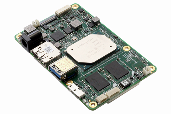
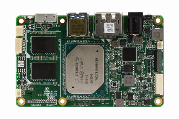
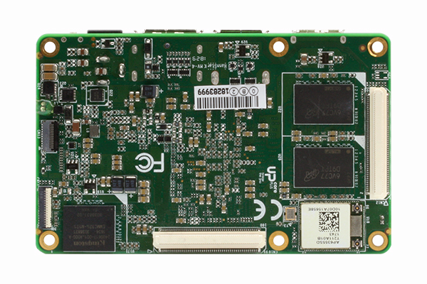
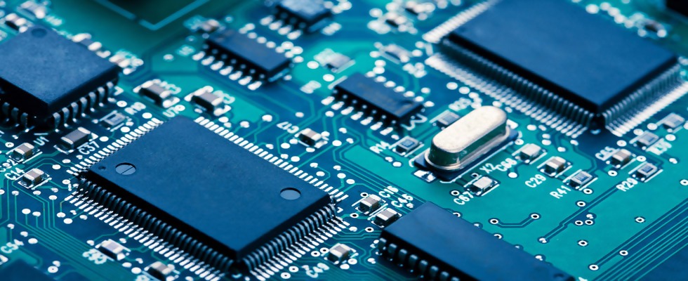
Today Printed Circuit Boards (PCBs) have become the integral part in many devices that we use in our daily lives. From handheld portable electronic devices, to industrial machines and heavy equipment, communication devices and consumer electronics we see everywhere these PCBs. Today’s PCBs are very complex and different shapes and materials based. They are flex and rigid and have variety of components that are wired together to perform a specific requirement. However this is only possible in the case of multilayer PCBs.

In older times the PCBs were only single or double layer and did only serve the purpose of simple computation or automation while today these PCBs are more advanced and multilayer and flex PCB are commonly found in motherboards, smart phones, smart watches, biomedical instruments, crypto currency mining devices, artificial intelligence based robotic circuits and many more. Also the manufacturing methods have improved in recent past enabling the faster production, cutting down production cost and reducing size of PCBs

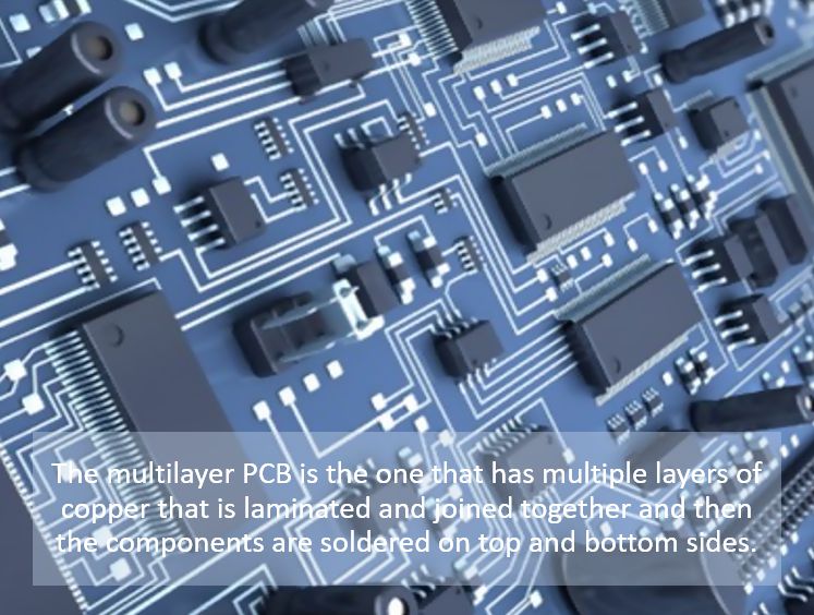
What Is a Multilayer PCB?

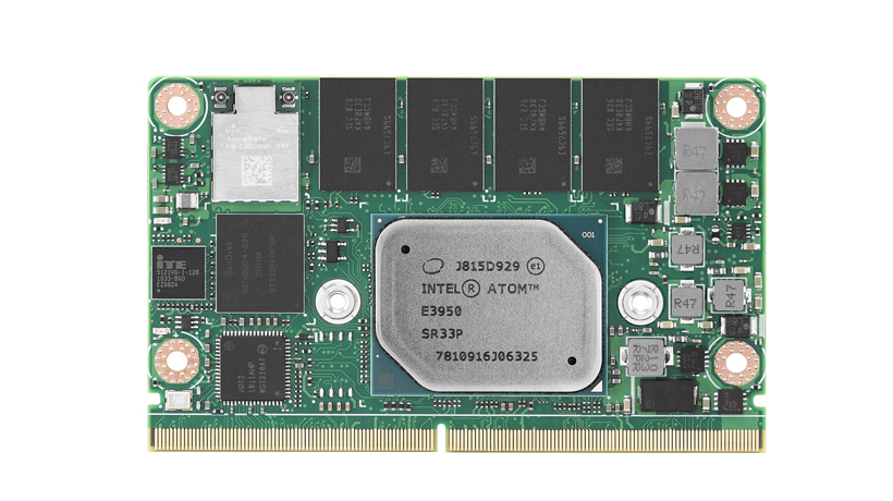
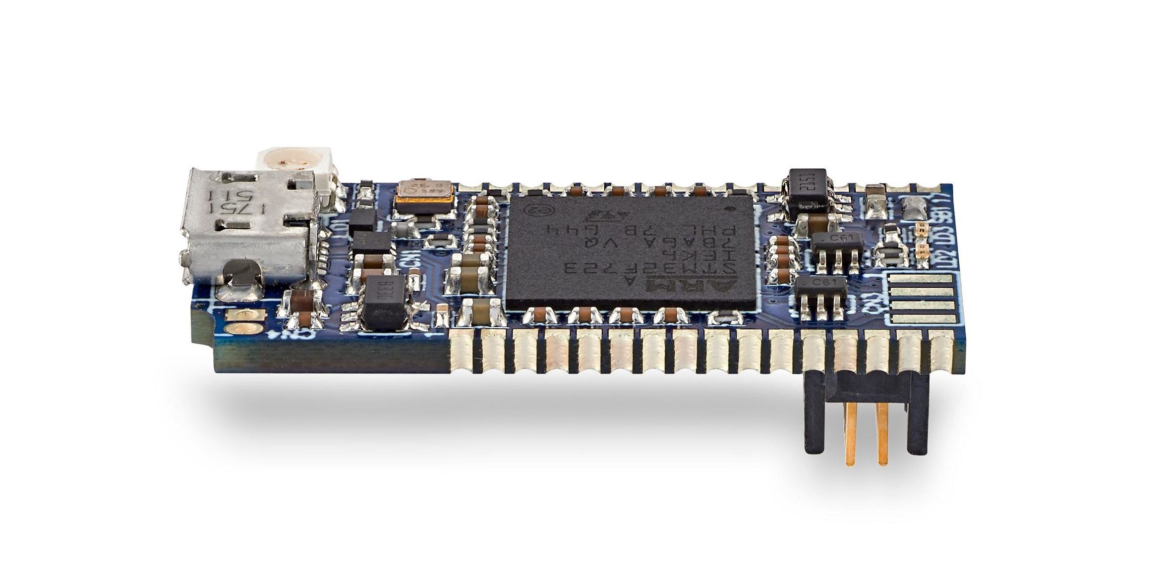
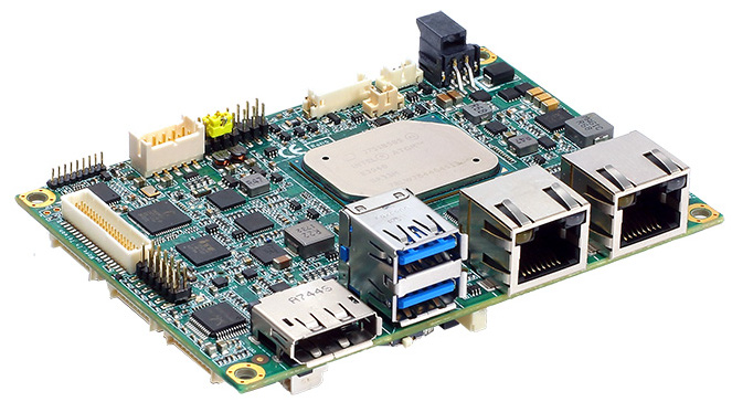
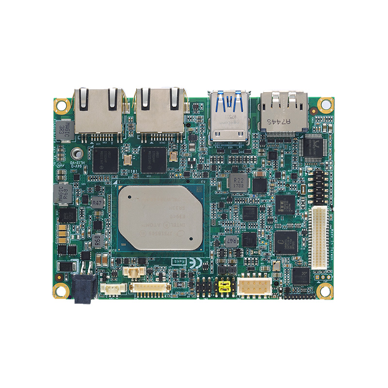
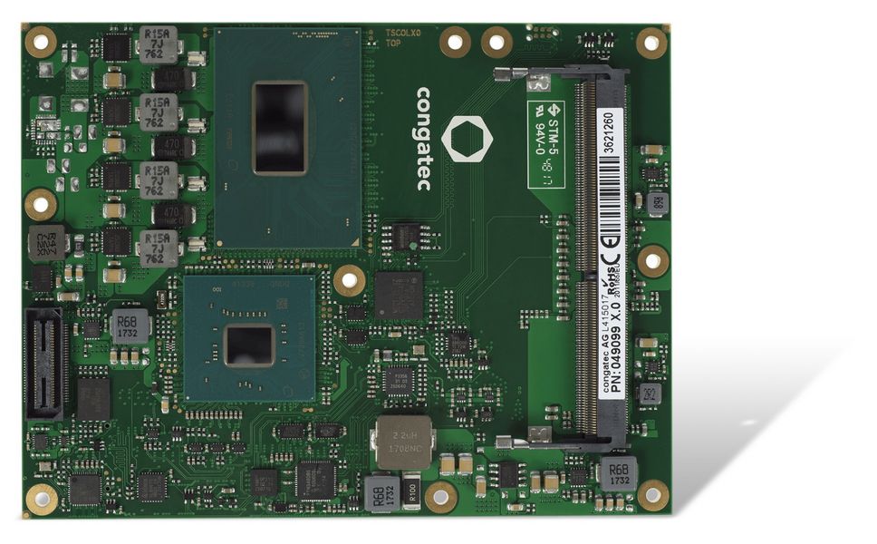
The multilayer PCB is the one that has multiple layers of copper that is laminated and joined together and then the components are soldered on top and bottom sides. The inner layers are actually the double sided circuit that are combined with each other to form one thick PCB with multilayers. The components are electrically connected by means of copper tracks and vias and pads/ holes join the interconnections. The vias are of different types like PTH, blind and buried. The result is the complex PCB with maximum circuitry on smaller PCB size.

Why Multilayer PCB is needed?

The advent of complex processing and evolving technology, demands the need of PCB layout procedure that can achieve the desired requirements. Also the problems that were occurring in the single or double sided PCBs like noise and stray capacitance was also an issue that caused the invention of multilayer PCB.

How many layers for Multilayer PCB:

The multilayer PCBs nowadaysare becoming widespread and available in very small form factor or sizes as compared to single or double sided PCBs. Their thickness also is variable and defendant upon number of layers. Commonly the multilayer PCBs are available from 4 layers to 12 layers depending upon the application and requirements. The layers are usually in even number say 4 layer PCB or 8 layer PCB, the odd numbered layers will cause problems of circuit wrapping and similar type issues. The multilayer PCBs are costly to produce as compared to single sided because of extra steps involved during PCB fabrication but their application are very huge. For example a smart phone can have a PCB with up-to 8 layers and a military electrical equipment can have a PCB with up-to 100 layers. This type of PCB with so many layers are very rare and costly.

Benefits of Multilayer PCB

There are many advantages of multilayer PCBs that are mainly due to technical perspective. They are as mentioned as below.

  • Miniature Size:

The most important advantage or we can say the most significant reason for the invention of multilayer PCB is it small size or form factor. The size is reduce due to multiple layers being stacked upon each other and connection by “vias”. This result in more compact, dense, solid and smaller sized PCBs like was never seen in past. These compact multilayer PCBs are increasingly used in mobile phones, laptops and wearable electronics.

  • Less weight:

The small size of PCBs will ultimately reduce the bulkiness of PCBs. So the multilayer PCBs are usually light weight and can be easily portable and used in handheld electronics.

  • High-Quality:

These multilayer PCBs are high quality in the sense that they are fabricated in a very well organized way and the amount of effort and work load invested in their fabrication is definitely more than that of single or double layer PCBs. Hence more quality and reliability results.

  • Durable:

The high pressure applied to bind the multiple layers with each other, high temperatures and heat environment through which these PCBs go during fabrication process and bonding agent and protective layers that make these PCBs solid and make them strong and durable.

  • More Density:

The density of a PCB is directly proportional to the amount of components soldered on a per unit size of PCB. For example 20 components placed on per square inch of PCB is denser than the PCB having 15 components per square inch. So the multilayer PCB most important advantage is its higher density as compared to its counterpart signal and double sided PCBs.

  • More Functionality:

As multilayer PCBs are denser hence more circuitry is incorporated in lesser PCB space, hence more computing and more powerful and speedy architecture is possible and highly demanded in high computation electronics like quantum computing, artificial intelligence, crypto currency mining machines, graphic cards and super computers

  • Ease of Installation:

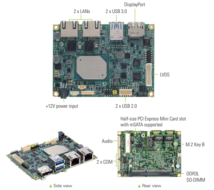
As we have seen in many old electronic equipment that the power supply section, video processing section and display driver sections of a TV were fabricated on separated PCBs. And they were integrated with each other via different connectors and sockets and complex wiring required. Nowadays, the LED TV comes in a PCB that has power supply, LED driver circuit and mother board all incorporated on a single PCB and single point of connection is required to install in the enclosure and lesser wiring / harness is required. This helps in ease of installation and dismantling the unit when repairs and troubleshooting is required.

Multilayer PCB Disadvantages

Along with many benefits discussed above for the multilayer PCBs, there are also disadvantages that are also vital to discuss. They are directly relevant to the applications that do not require much more complex circuits and are lower in cost. The disadvantages are mentioned as under

  • Multilayer PCBs are Costly:

Yes the multilayer PCBs are very costly as compared to the single of double sided PCBs. This is because the manufacturing process is complex and requires much more labor and time. Also the assembling of these PCBs is a complex job hence more man hours are required thus raising the cost of PCB. Also the machinery required for fabrication / manufacturing of multilayer PCBs is very expensive and classical. Moreover, any smallest error in the design or during fabrication can lead to the complete failure of PCB resulting in scrap and wasting time and money. All these factors contribute to relatively increase production cost of multilayer PCBs.

  • Inspection is Complex:

As discussed above, the slightest flaw in the design can lead to the PCB useless and scrap. Hence more careful manual and automated inspection required that turns out to be complicated work.

  • Multilayer PCB Manufacturers are Limited:

The main problem in the multilayer PCBs is its manufactures availability and capacity. Many manufacturers cannot bear the capacity and expenses of costly machinery like AOI and laser machines, so they would not give that quality of PCB as the user require. Some manufactures do not work on multilayer PCB fabrication at all but only work on single and double sided. So you must be careful while choosing your contractor for multilayer PCB fabrication

  • Professional Design Engineer is required:

For Multilayer PCB, the design must be lay out by a professional engineer who has experience in multilayer PCB layout design. There are numerous problems that can result if design is not carefully made. Some of them are high speed circuit’s noise, stray capacitance, impedance mismatch, improper thermal pads and grounding etc

  • Manufacturing Time is long:

The multilayer PCBs are complex to manufacture that ultimately leads to longer manufacturing time. So overall the customer would receive his PCBs with delays in manufacturing. Especially if some issue or problem arises in design or manufacturing process then it has to be reverted to design or fab house to eliminate the error and fabricate again.

Multilayer PCBs VS Single Layer

As discussed above advantages and disadvantages of multilayer PCBs, we have understood the difference between two main types of PCBs. Some major difference or comparison between the two are as follows

  • Multilayer PCBs are more dense than Single Layer:

The multilayer PCB can accommodate more components on a specific area on PCB as compared to single layer PCB resulting in more advance and complex circuitry.

  • Smaller Size:

Multilayer PCBs are small in size due to denser PCB as compared to single sided PCB

  • Less Weight:

Small size means less weight and more portability and easy to handle. Single sided PCBs are bulky and used in large electronic / electrical equipment

  • Enhanced Design Functionality:

More circuitry in lesser space, will ultimately increase more functionality as compared to single sided PCBs. This is more favorable in today’s advance electronics industry.

What to Choose Single Sided or Multilayer:

This all depends on your application. If you need a product to be lesser weight and smaller with more electronic circuitry then go for multilayer or if you want a product where size is not a matter than go for single sided PCB.

Multilayer PCB Applications

  • Consumer Electronics:

The term “Consumer Electronics” is a wide term that includes many electronic devices that comes under the umbrella of commonly used devices that are directly relevant to common users like you and me. The consumer electronics include, smartphones, smart watches, calculators, TV remote control, mp3 music player, toys, kitchen appliances, washing machines, electric kettle, e-cigarettes, LED bulbs and energy savers etc

  • Computers and Devices:

Today our world is highly dependent on computers and automation. Multilayer PCBs are commonly found in computers and associated products like motherboards, graphics cards, EEPROMs, Power supplies, keyboard, computer mouse, ADCs, GPUs, Image processing circuits etc

  • Telecommunication Electronics:

The industry of telecommunication is very huge that includes many electronic devices and equipment that contain sophisticated electronics and can contain multilayer PCBs up-to 8 layers. Some of the applications of telecommunication electronics is GPS, satellite, computer servers, GPRS, communication towers, Radar electronics, Sonar / Lidar, Antenna, Power amplifier, filter, PLLs, Mixers, Attenuators, LNA, on board telemetry and telecommand processing circuits etc

  • Industrial Automation:

The electronics operating under industrial environment faces harsh and stressing factors like heat, temperature, pressure, shocks, vibration, dust and humidity. Thus PCB with solid form and rigidity is essentially required and that type of PCB is multilayer PCB. Some of the application of industrial electronics are robotics, automated assembly lines, car manufacturing, spray painting robots, packaging conveyer belts, PLCs

  • Medical Devices:

The electronics is the integral part in the medical devices and sensitive equipment being used to monitor patients and serve patients. These devices are usually portable and handheld like ECG/EEG machines, blood pressure measuring device, electronic sugar testing device and infrared temperature monitoring. Moreover large equipment using nuclear, radiology, MRI, CT scan machines and X-Ray machines very widely use multilayer PCBs.

  • Military, Aerospace and Defense:

Unmanned Aerial Vehicles (UAV), Unmanned Ground Vehicle (UGV), Radar, Surveillance, Automated Guns, Rail Gun, Navigation systems, Aircraft defense system and avionics, satellite control facility, satellite tracking system, Airplane auto pilot, artificial intelligence used in cyber security of military hardware are the major examples of utilization of multilayer PCBs in the equipment pertaining to above mentioned fields. These PCBs are assembled with Mil spec components that are rugged and can withstand harsh environment of space and upper atmosphere where high pressure and temperature conditions could damage custom grade components. So these multilayer PCBs along with tough components can meet the stringent requirements of military, aerospace and defense.

Conclusion

With the emerging needs of modern technology as mentioned in above different types of industries and applications, the need of multilayer PCBs is increasing day by day. This multimillion dollar industry is rapidly increasing due to huge demands in the sector that can pay more money to achieve their goals of small size, light weight, durable, rugged and complex functionality products. While on the other hand, these multilayer PCBs are costly, requires more man hours and time, fabrication / manufacturing process is complicated but that all rules out the fact that people in those above mentioned industries are willing to pay more and can wait more for the exquisite product to be developed that will eventually pay off and completely satisfy customer with all aspects as required.

Advantech Launches the New SMARC Module with Intel® Atom™/Pentium®/Celeron®

Advantech, a leading embedded computing solutions provider, is happy to announce the launch of its first SMARC module: the SOM-2569. SMARC (Smart Mobility Architecture) is a versatile small form factor computer module targeting applications that require low power consumption, the flexibility to upgrade computing performance, and effective budget control in the system development process. Together with bundled the WISE-PaaS/DeviceOn software, SMARC modules can help end customers with operations management and ease maintenance.

The SOM-2569 SMARC module features Intel® Atom™ E3900, Pentium™ and Celeron™ N Series processors. Its offers a small size — 82mm x 50mm — and supports up to three displays simultaneously. On top of offering multi-display, it also supports several I/O, such as SATA, USB3.0/2.0, COM port, SMBus, and I2C.

There are three key features of the SOM-2569:

  • 2 LAN controllers and an onboard Wi-Fi module
  • TPM and secure boot for enhanced security
  • onboard design for all key components (e.g. memory, eMMC) for maximum reliability

All these features help ensure that the SOM-2569 is highly suitable for automation applications.

Wi-Fi and Dual LAN Controllers: Connectivity Made More Flexible Than Ever

Connected devices are the fundamental elements of modern smart factories. SOM-2569 is integrated with Wi-Fi and Bluetooth onboard, and the dual 1000base-T interfaces to meet both wireless and cable connectivity requirements. With Wi-Fi and Bluetooth in the onboard module, SOM-2569 is compliant with IEEE 802.11 a/b/g/n/ac PCIe Wi-Fi & Bluetooth 4.2 and RF certification. Through its rigorous design and testing processes, Advantech not only offers better wireless signal integrity and compatibility, but also save time for system integration.Moreover, SOM-2569 includes two LAN controllers that support two RJ45 ports. The combo design provides the flexibility in various factory applications where isolated network domains are necessary for security and reliability reasons. For example, when the wireless LAN connects to an outside network and the wired LAN can connect to two different local area networks simultaneously.

TPM2.0 and UEFI Secure Boot: Eliminate Risk of Cyber Intrusions TPM2.0 and UEFI Secure Boot:

Reducing the risk of Cyber attacks TPM (Trusted Platform Module) is defined by the “Trusted Computing Group” based on a publicly available specification. The hardware chip enables system protection; encompassing secure data storage, platform integrity reporting, and platform authentication.

The UEFI security boot offers a process to ensure that your computer boots up using only software that is trusted by the manufacturer. When the computer starts, firmware checks the signature of each piece of boot software, including firmware drivers (Option ROMs) and the operating system. If the signatures are good, the PC boots and the firmware gives control to the operating system.

All Components Soldering Down: Robust and Reliable

SOM-2569 has soldering down all components, including CPU, memory, storage and wireless chips. Soldered components provide robust and reliable characteristics to work in harsh environment. It passed tests including vibration at 0.028G²/ Hz, 3.5 Grms, bumping at 1 corner, 3 edges, 6 faces, and thermal shock resistance, ranging from -40°C to 85°C at slope 10°C per minute, etc. With Advantech rigorous validation, proves SOM-2569 is a perfect fit to use in harsh environment.

SOM-2569 Features

  • SMARC V2.0 specification compliance
  • Intel® Atom™ E3900 & Pentium™ and Celeron™ N Series processors
  • Wi-Fi / Bluetooth module onboard
  • TPM2.0 & UEFI secure boot for system protection
  • Two independent LAN chips for 1000Base-T data transmission
  • 32G eMMC
  • 8GB LPDDR4 memory
  • Operating Temp: 0°C ~ 60°C or -40°C ~ 85°C

more information: www.advantech.de

Compact debug probe accelerates STM32 application development

The STLINK-V3MINI probe combines the enhanced features of STLINK-V3SET with standalone simplicity for faster programming and ease of use, for an even more affordable price, at just $9.75.

The compact, portable probe can be used anywhere to upload and debug applications on STM32 microcontrollers. It leverages ST’s 14-pin STDC14 debug cable to support enhanced features including Virtual COM Port (VCP). VCP brings extra convenience and flexibility, such as easily observing runtime data on the host PC for faster, clearer debugging. Mass-storage support is another feature of STLINK-V3MINI that makes developers’ lives easier by enabling the uploading of files directly through the probe with a simple drag and drop to quickly trial new ideas or run various demo applications. Moreover, STLINK-V3MINI comes with reference files for 3D printing that let owners create their own customized casing for the probe. STLINK-V3MINI interacts smoothly with the STM32CubeProgrammer and is directly supported in popular commercial IDEs including Keil MDK-ARM, IAR EWARM, and GCC-based IDEs including free STM32CubeIDE from ST. In addition, ST provides free access to the probe’s low-level APIs to help integrate STLINK-V3MINI in custom test platforms.

Key Features

  • Stand-alone probe
  • Approximately 15 x 30 mm high-density integration PCB
  • Delivered with 1.27 mm pitch STDC14 debug connector and STDC14 to STDC14 flat cable
  • Self-powered through a USB connector (Micro-B)
  • USB 2.0 high-speed compatible interface
  • Direct firmware update support (DFU)
  • JTAG / serial wire debugging (SWD) specific features:
    • 3 V to 3.6 V application voltage support and 5 V tolerant inputs
    • JTAG communication support
    • SWD and serial wire viewer (SWV) communication support
  • Virtual COM port (VCP) specific features:
    • 3 V to 3.6 V application voltage support on the UART interface and 5 V tolerant inputs
    • VCP frequency up to 15 MHz
  • Drag-and-drop Flash programming
  • Two color LEDs: communication, power
  • Includes STDC14 signals protection

STMicroelectronics – www.st.com

Apollo Lake Pico-ITX SBC supplies mini-PCIe and M.2 expansion

Axiomtek – a world-renowned leader relentlessly devoted in the research, development and manufacture of series of innovative and reliable industrial computer products of high efficiency – is pleased to introduce the PICO319, a low power yet powerful fanless Pico-ITX SBC powered by the onboard Intel® Atom® x5-E3940 quad-core processor (code name: Apollo Lake). The noise-free pico-ITX motherboard offers combinations of ruggedness, high computing capabilities and enhanced graphics capability in an extremely compact size of only 100 x 72 mm. Moreover, the board features 12V DC power supply input with AT Auto Power On function. It brings a solid and standardized platform for industrial automation, transportation and retail applications.

The tiny 2.5-inch embedded board PICO319 comes with one 204-pin DDR3L-1867 SO-DIMM socket for up to 8GB of system memory. A dual-display capability is available through DisplayPort and 18/24-bit single/dual channel LVDS ports. For extensive storage needs, this compact embedded motherboard has one M.2 Key B slot (22 x 42 mm or 30 x 42 mm) for SATA or PCIe x2 SSD card and one half-size PCI Express Mini Card slot in support of mSATA.

“The PICO319’s fanless and ultra-compact design allows easy installation in space-constraint environments and more flexible product designs. The 2.5” embedded board provides various expansion interfaces within its limited dimensions including an M.2 Key B slot for a cellular module and a half-size PCIe Mini Card slot for a wireless module, which offers diversity and flexibility for application integration. In addition, the board comes with two Gigabit Ethernet ports with Intel® Ethernet Controller I211-AT in support of Wake-on-LAN and PXE Boot ROM,” said Michelle Mi, a product manager of Product PM Division at Axiomtek. “ Axiomtek’s PICO319 can operate under wide temperature settings ranging from -40 to 70°C, making it an ideal solution for use in rugged and harsh environments.”

The Intel® Atom®-based pico-ITX board comes with rich I/O connectors, including two USB 2.0 ports, two USB 3.0 (USB 3.1 Gen1) ports, one RS-232/422/485 port, one RS-232 port, one HD Codec audio, and 4-channel digital I/O. It also supports SMBus that is compatible with I2C for smart battery support. The PICO319 offers watchdog timer and hardware monitoring function for reliable operation.

Advanced Features:

  • Intel® Atom® x5-E3940 processor (code name: Apollo Lake)
  • One DDR3L SO-DIMM for up to 8GB of memory
  • Two USB 2.0 and two USB 3.0 (USB 3.1 Gen1)
  • One PCIe Mini Card slot in support of mSATA
  • One M.2 Key B for SATA
  • Features 12V DC power supply input with AT Auto Power On
  • Extended operating temperature ranging from -40 to 70°C

Axiomtek’s PICO319 will be available in August 2019. For more product information or customization services, please visit our global website at www.axiomtek.com or contact one of our sales representatives at info@axiomtek.com.tw.

The PICO319 will be available in August at an undisclosed price. More information may be found in Axiomtek’s PICO319 announcement and product page.

Congatec presents 10 new high-end modules for embedded edge computing

congatec – a leading vendor of standardized and customized embedded computer boards and modules – today announced 10 new COM Express Type 6 modules featuring the best and latest Intel® embedded processor technology. The four Intel® Xeon®, three Intel® Core™, two Intel® Celeron® and one Intel® Pentium® processors are all based on the same Intel microarchitecture (codenamed Coffee Lake H). This enables congatec to provide all 10 new processors on one COM Express module design – the conga-TS370. A total of 14 processor module variants are now available on this single microarchitecture, offering extremely wide scalability. The spearhead in terms of computing power is the 45 watt 6-core module with 2.8 GHz Intel® Xeon® E-2276ME processor. It provides the highest embedded computing performance with integrated high-performance processor graphics currently available worldwide, while the 2.4 GHz Intel® Celeron™ G4930E processor module with 35 watts sets the new price-performance benchmark.

Particularly noteworthy are the two 6-core congatec modules with a TDP of 25 watts offered on Intel® Xeon® E-2276ML and Intel® Core™ i7-9850HL processors. They enable developers to create completely passively cooled embedded edge computing systems that can run up to 12 standalone virtual machines in parallel thanks to hyperthreading. This allows operation even in fully sealed systems, under the harshest environmental conditions and with the highest IP protection. The same applies to the two quad-core modules with Intel® Xeon® E-2254ML or Intel® Core™ i3-9100HL processor as well as the Intel® Celeron® G4932E processor-based module, all featuring a – partly configurable – TDP of 25 watts.

“In the embedded edge computing segment, our OEM customers are now using such multicore platforms to consolidate several formerly separate systems on a single embedded edge computer. Hypervisor technology allows them to operate up to 12 virtual machines in parallel on one system,” explains Andreas Bergbauer, Product Line Manager for COM Express Modules at congatec. “These include real-time controllers (soft PLCs), Industry 4.0 gateways for tactile Internet via Time Synchronized Networking, IoT gateways for sending big data towards the cloud and central management systems, as well as vision systems, artificial intelligence (AI) and deep learning applications. In addition, there are software-defined networking functions such as intrusion prevention and detection systems that analyze data traffic parallel to the applications, thereby avoiding latencies that would arise with serial operation of analytics and applications.”

Other applications besides embedded edge computing include, of course, classic high-end medical imaging systems and HMIs as well as high-end gaming, infotainment and digital signage systems that require best-in-class computing power and throughput on a single die in tandem with the Intel® graphics technology.

The updated Conga-TS370 and Conga-TEVAL/COMe 3.0 carrier are available now at undisclosed prices. More information may be found in Congatec’s update announcement, as well as the Conga-TS370 and Conga-TEVAL/COMe 3.0 product pages.

Beyond 5G: Wireless Transceiver With Ultra-Fast Data Processing

UCI Professor of Electrical Engineering & Computer Science Payam Heydari’s lab engineered a new wireless transmitter and receiver. pictured are Heydari, Huan Wang, and Hossein Mohammadnezhad
photo: Steve Zylius/UCI

A new wireless transceiver invented by electrical engineers at the University of California, Irvine boosts radio frequencies into 100-gigahertz territory, quadrupling the speed of the upcoming 5G wireless communications standard. by Jens Nickel @ elektormagazine.com

Labeled an “end-to-end transmitter-receiver” by its creators in UCI’s Nanoscale Communication Integrated Circuits Labs, the 4.4-millimeter-square silicon chip is capable of processing digital signals significantly faster and more energy-efficiently because of its unique digital-analog architecture. The team’s innovation is outlined in a paper published recently in the IEEE Journal of Solid-State Circuits.

UCI Professor of Electrical Engineering & Computer Science Payam Heydari’s lab engineered a new wireless transmitter and receiver. pictured are Heydari, Huan Wang, and Hossein Mohammadnezhad
photo: Steve Zylius/UCI

His group’s answer is in the form of a new transceiver that leapfrogs over the 5G wireless standard – designated to operate within the range of 28 to 38 gigahertz – into the 6G standard, which is expected to work at 100 gigahertz and above.

“The Federal Communications Commission recently opened up new frequency bands above 100 gigahertz,” said lead author and postgraduate researcher Hossein Mohammadnezhad, a UCI grad student at the time of the work who this year earned a Ph.D. in electrical engineering & computer science. “Our new transceiver is the first to provide end-to-end capabilities in this part of the spectrum.”

read more: news.uci.edu

1.12″ 96×96 OLED Full Color Display Panel with SPI

DM-OLEDC112-656 is a 1.12″ 96×96 OLED Full Color Display Panel with SPI MCU interface for easy integration.

Main features

  • Active Matrix Full Color OLED
  • 1.12″  96×96 Pixels
  • Interface: 8bit 68XX/80XX MCU, 4-wire SPI
  • Drive IC: SEPS114A

You can buy the module for $4.95 on www.displaymodule.com

Latest Solutions from CUI & Digi-Key by OEMSecrets.com

Interconnect Solutions

Screw Type Terminal Blocks

CUI’s screw type terminal block connectors offer wire gauges ranging from 26 AWG to 10 AWG and horizontal, vertical, and 45° orientations. With operating temperature ranges from -40°C to +105°C and 5 mm, 5.08 mm, and 7.62 mm pitches, CUI’s low cost screw type terminal blocks are well suited for a range of interconnect needs. Learn More ►

IP67 Rated Audio Jacks

Conforming to the 3.5 mm audio standard, CUI’s waterproof audio jack connectors carry Ingress Protection (IP) ratings of IP67 to deal with the harsh conditions found in industrial and outdoor applications. The models are available in surface mount, mid mount SMT, and through hole mounting styles with 12 VDC rated operation, 1 A current ratings, and profiles as low as 5.6 mm. Learn More ►

Audio Solutions

IP Rated Audio Solutions 

CUI’s waterproof speakers, microphones and buzzers offer Ingress Protection (IP) ratings up to IP68, diameters as small as 4 mm, and depths as low as 1.5 mm. With a multitude of configurations and options, these IP rated audio solutions deliver the durability and performance needed to withstand harsh, high moisture environments. Learn More ► 

MEMS Microphones

CUI’s MEMS microphones provide users with improved audio quality and performance in compact, low profile packages as small as 2.75 mm x 1.85 mm x 0.95 mm. Featuring sensitivity ratings from -44 dB up to -26 dB, signal to noise ratios from 57 dBA up to 65 dBA, and sensitivity tolerances as low as ±1 dB, these MEMS microphones are ideal for a range of portable consumer electronics applications. Learn More ►


Power Solutions

Encapsulated AC-DC Power Supplies from 2 W – 25 W

With compact footprints and 4 kVAC isolation, CUI’s PSK series of encapsulated AC-DC power supplies from 2 W to 25 W are housed in board-mount, chassis-mount, wire-lead, and DIN rail packages. The modules operate at temperature ranges of -40°C up to +85°C at full load, making them ideal for a range of space-constrained applications. Learn More ►

10 W Isolated DC-DC Converters 

Outputting up to 10 W of continuous power, CUI’s range of open frame and encapsulated PYBJ10 isolated DC-DC converters deliver a 4:1 input voltage range and up to 88% efficiency. Ideal for convection-cooled equipment and a range of other applications, CUI’s PYBJ10 series features a -40°C to +85°C operating temperature range with over voltage, over current, and short circuit protections. Learn More ►

Thermal Management

DC Axial Fans with omniCOOL™ System

CUI’s CFM-V series of high-performance axial fans deliver superior forced air cooling performance and longer operational life compared to traditional sleeve bearing designs thanks to their innovative omniCOOL system. With airflows ranging from 5.4 CFM in the 40 mm series up to 138 CFM in the 120 mm series, these DC axial fans feature noise levels from 10.7 dB to 48 dB, making them ideal for a variety of IT and telecommunication equipment, medical devices, and industrial applications. Learn More ► 

High Performance Peltier Modules with arcTEC™ Structure 

CUI’s line of high-performance thermoelectric modules delivers superior cooling performance and a longer cycle life with its innovative arcTEC structure. Ranging in size from 20 mm to 50 mm with profiles as low as 3.15 mm, these Peltier modules are available with a ΔTMAX up to 95°C (Th=50°C) and current ratings from 2.0 A to 12.5 A. Learn More ►

TOP PCB Companies