SparkFun has released the company’s first open-source, embedded-systems module—SparkFun Artemis, Engineering Version—to empower engineers, prototypers, and R&D teams to integrate the TensorFlow machine-learning platform into any design. via www.open-electronics.org
Additionally, the team has launched three boards with the unshielded module: BlackBoard Artemis,BlackBoard Artemis Nano, and BlackBoard Artemis ATP.
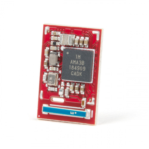
Built around the ultra-low-powered Ambiq Micro Apollo 3 processor, and powered by a single coin cell battery, it let you run machine learning models locally. No cloud needed.
The module has all of the support circuitry needed to make use of the Apollo 3 processor, but has been designed so that routing to the module can be done with lower-cost 2-layer PCBs with an 8 mil trace clearance. That means it can be easily integrated into maker projects.
SparkFun Artemis module is the first open source hardware module with the design files freely and easily available here. The flexibility of the Artemis module starts with its Arduino core. You can program and use the Artemis module just like you would an Uno or any other Arduino.
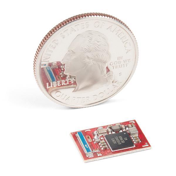
Beyond its small size (15.5 x 10.5mm including antenna), key features of the ultra-low-power Artemis module include:
Cortex-M4F based BLE module using the Apollo3 microcontroller from Ambiq
Advanced HAL (hardware abstraction layer) allowing users to push the modern Cortex-M4F architecture
Capability of running machine learning algorithms with the low current consumption of 6μA/MHz at 3.3V
Integrated Bluetooth 5 low-energy radio and 2.4GHz antenna
All necessary circuitry for easy integration—large SMD pads and spacing allow for low-cost 2-layer carrier board implementations; programming over pre-configured serial bootloader or JTAG
Every serious maker out there will surely tell you the importance of having a good oscilloscope. An oscilloscope is something you should have if you really consider yourself a maker, and fortunately enough, the cost of quality oscilloscope has been on the decline for some time now, so you don’t necessarily have to get the big bucker ones to get started.
Small size PC based USB scopes are an excellent alternative, and they do feature a host of capabilities that will give you the performance, accessibility, portability you will need and also cost-effectiveness as a maker. We could possible underestimate the potential of a PC-based USB oscilloscope because of the sheer small size as compared to benchtop versions. But as the processing power available on today’s PCs is increasing, high-end USB PC-based scopes are sprouting out which are increasing rivaling their benchtop partners and even with the advantage of a lower cost.
Not only are PC based scopes significantly easy to use, but the idea of using a PC for the processing means, user can do more with the files, write a custom program to interface with the scope to maximize the full scope potential and many more. In this article, we will mention some lovely USB based scopes (not in any order) for every maker, thinkers, and upcoming electronics engineers.
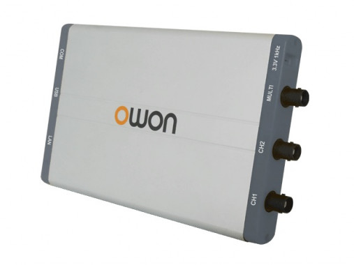
The Owon VDS1022I features a 25 MHz bandwidth and maximum 1 GS/s real-time sample rate
The Owon VDS1022I is a PC based scope from the Chinese manufacturer Owon that features a 25 MHz bandwidth and maximum 1 GS/s real-time sample rate. The scope is a multi-channel oscilloscope (2+1) channel with a multi-trigger option: Edge, Video, Slope, Pulse, and Alternate. One exciting feature about the scope is that it is capable of displaying two separate waveforms on the same screen.
The scope includes isolated USB for protection, RS232 port, USB port, LAN port, and a probe compensation. The scope is available for purchase for about $104 on Amazon
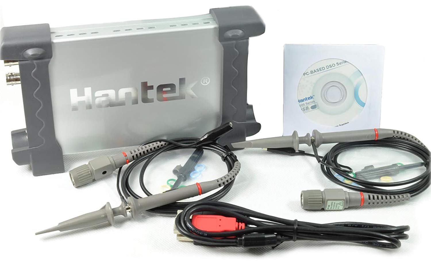
The Hantek HT6022BE is an inexpensive PC based scope for the maker on a budget. The PC based scope is capable of 20 MHz of bandwidth, a multi-channel scope, 48MS/s sampling rate, and quite portable allowing for easy carry. The Hantek HT6022BE cost around $65.55 and available for purchase on Amazon.
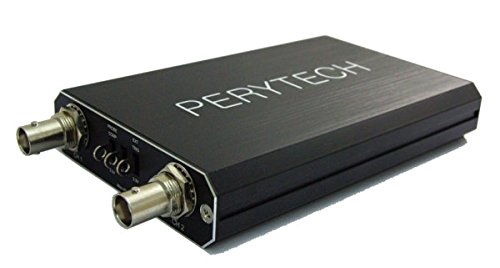
The Perytech DSO U2200 USB oscilloscope carries a price tag of $110 and also comes with a slight software design from the conventional window design to a more oscilloscope like environment allowing it to be easy to use without the need of manuals. One significant advantage of the Perytech scope as compared to others is its productive software environment with features automatic measuring functions, including maximum value, minimum value, frequency, and period. A stacking function allows up to four USB oscilloscopes to be stacked as an eight-channel oscilloscope.
The scope also features logic analyzer, and the PC based scope is capable of 60MHz Bandwidth with a sampling rate of 240 MS/s. The scope is available for purchase on Amazon.
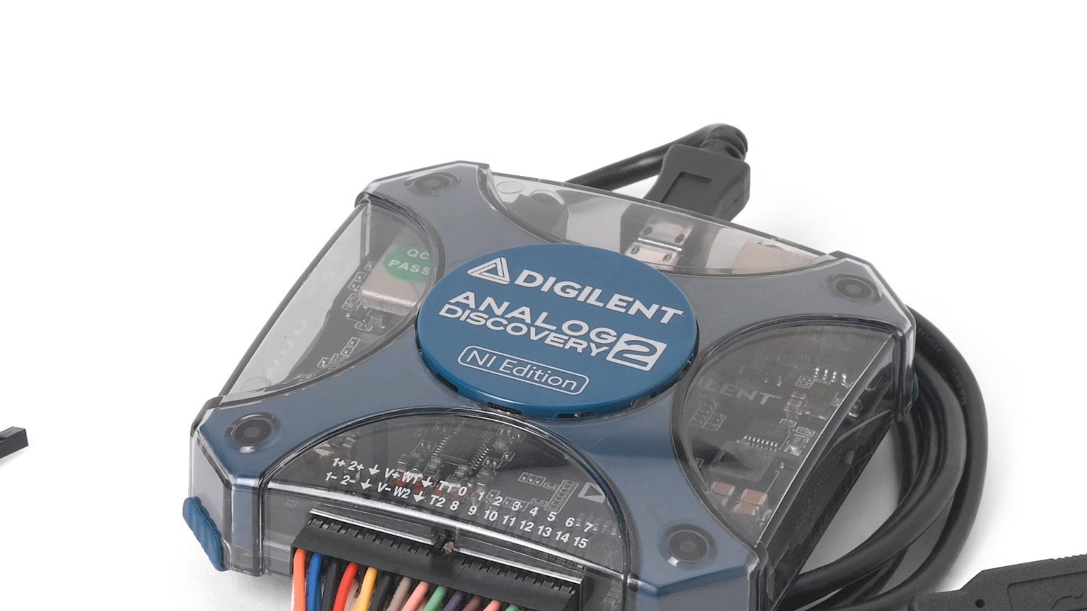
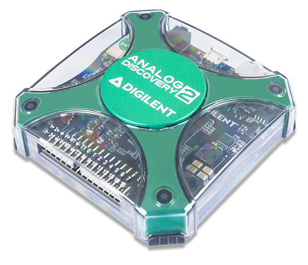
The Digilent Analog Discovery 2 is a product of Analog Devices. It’s a multi-function USB oscilloscope which is highly designed for students, enthusiasts, makers, and hobbyists. It allows them to measure, visualize, simulate, and analyze a variety of mixed-signal circuits. The Analog Discovery 2 transforms any PC into an electrical engineering workstation. This USB-powered device enables students to build and test analog and digital circuits in any environment with the functionality of traditional benchtop instruments.
The scope is a multi-channel (2 channel) oscilloscope with a two-channel waveform generator, a 16-channel logic analyzer, 16-channel digital pattern generator, and protocol analyzer. Features include two analog inputs (±25 V, differential, 14-bit, 100 MS/s, 30-MHz+ bandwidth),two analog outputs (±5 V, 14-bit, 100 MS/s, 12-MHz+ bandwidth), a stereo audio amplifier to drive external headphones or speakers with replicated arbitrary waveform generator (AWG) signals, 16 digital I/O (3.3-V CMOS and 1.8-V or 5-V tolerant, 100 MS/s), and two I/O digital trigger signals for linking multiple instruments (3.3-V CMOS).
Its WaveForms Software Development Kit comes with C++ and Python libraries and examples as well as forum support from the software developers. Analog Discovery 2 is also supported by third-party software such as MATLAB and LabVIEW. The scope is available for purchase for about $280 here. A student version is available for $183 from National Instruments
Hantek IDS1070A WIFI USB 70MHz 2Channels 250MSa/s Storage Oscilloscope Suitable for iOS Android PC System
Hantek IDS1070A is a multi-channel oscilloscope that can be used with iOS, Android 4.0, and Windows XP or higher on tablets, PCs, and the iPhone. Communication with the scope and its host is through WLAN while the USB port is for battery charging and USB connection to PC instead of Wireless mode. It cost around $126 and feature a 70 MHz bandwidth and a real-time sampling rate of 250 MS/s. T
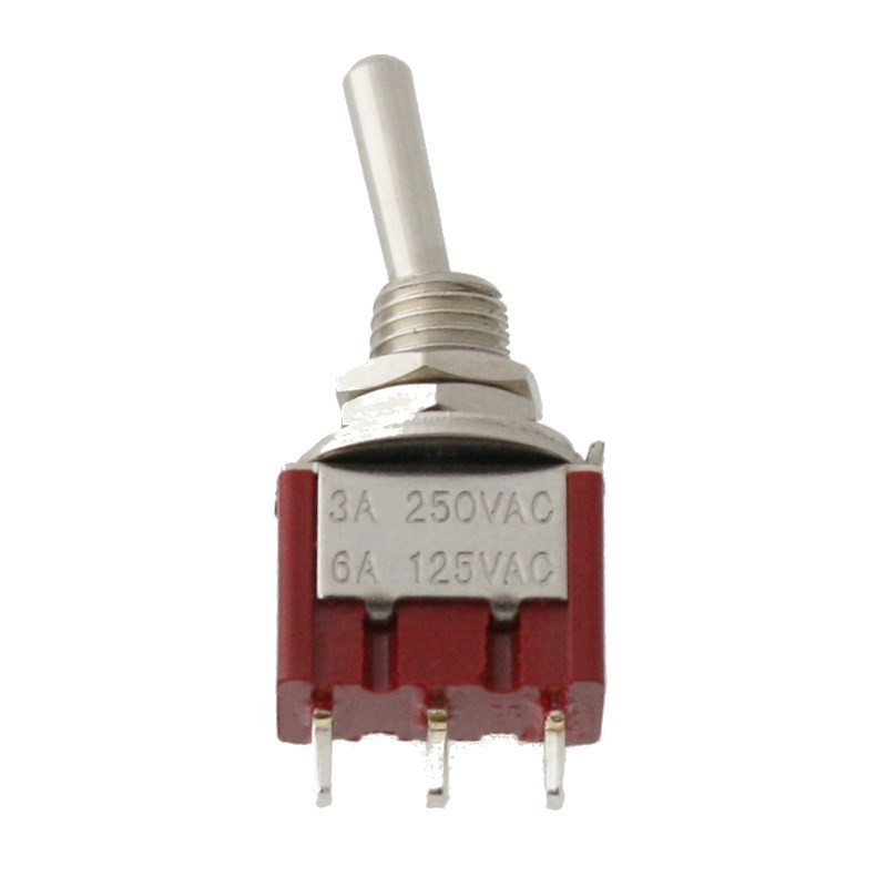
Latching Toggle switches are one of the most popular kinds of switches, from their use by kids in basic electricity classes to their use in prototypes and more advanced products, they provide a familiar and reliable way to close or open a circuit. This makes them the go to switch for designers in most applications but while they may be perfect for switching your device on/off in a low volume project, their price does not make them worthy for use in large scale projects as they can be expensive (usually >$1 depending on the current rating you require), comparing the fact that you could buy a microcontroller and other components for that price. Due to these costs, designers, have been replacing (where possible) the toggle switch with the momentary push buttons which are way more cheaper especially when you are trying to get the cost down on your product.
For today’s project, I thought it will be a good idea to look at the latching toggle switch to see if we can create a cheaper alternative which can be used for ON/OFF switch operations in devices in large scale production. One of the major factors behind the cost of the latching toggle switch is that they are mechanical in nature, thus for our solution, we will ensure we don’t turn the same part by creating a soft latching switch circuitry but we will use a push-button instead.
Simple Soft Latch Switch using Push-Button – [Link]
Latching Toggle switches are one of the most popular kinds of switches, from their use by kids in basic electricity classes to their use in prototypes and more advanced products, they provide a familiar and reliable way to close or open a circuit. This makes them the go to switch for designers in most applications but while they may be perfect for switching your device on/off in a low volume project, their price does not make them worthy for use in large scale projects as they can be expensive (usually over a dollar depending on the current rating you require), comparing the fact that you could buy a microcontroller and other components for that price. Due to these costs, designers, have been replacing (where possible) the toggle switch with the momentary push buttons which are way more cheaper especially when you are trying to get the cost down on your product.
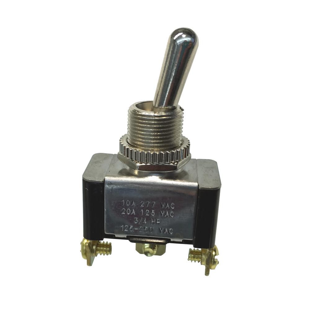
A Toggle Switch
For today’s project, I thought it will be a good idea to look at the latching toggle switch to see if we can create a cheaper alternative which can be used for ON/OFF switch operations in devices in large scale production. One of the major factors behind the cost of the latching toggle switch is that they are mechanical in nature, thus for our solution, we will ensure we don’t turn the same part by creating a soft latching switch circuitry but we will use a push-button instead.
Design Requirements
As with any design, we will start out by outlining the requirements for our Soft Latching Switch. All of the requirements are geared towards ensuring the cost is kept low and performance is either greater or of the same quality with the mechanical latching toggle switch. The requirements are:
Standalone; The circuitry should be independent of the system in which it is to be deployed.
Minimal Parts; It should use very little components to keep the size small and cost as low as possible.
Basic Parts Only; We won’t be using any special/dedicated modules
No current drawn when Off
Cheaper than the mechanical latching toggle switch.
Designing the Switch
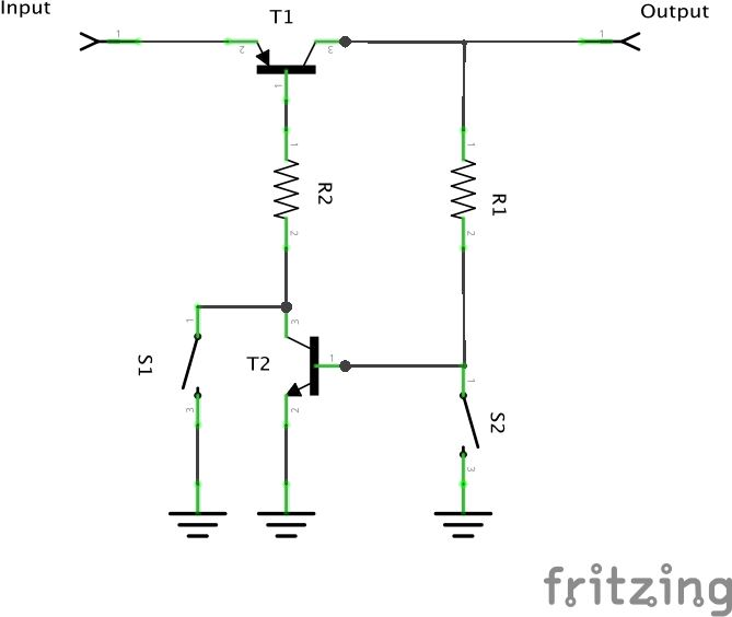
For today’s design, we will draw inspiration from a design by David Jones. The switch circuitry (shown in the schematics below) is made up of two transistors which could either be PNP or NPN. The transistors work hand in hand such that the flow of base current to turn “ON” one of the transistors turns ON the other transistor. To explain better, consider the schematics below.
Two Switch On/Off Circuit
When the circuit is initially powered up, a chicken and egg kind of situation will be experienced as the transistor T2 will be off because there is no base current flowing through T1 (T1 is off) since the switch S1 has not been pressed. When the “on” Switch(S1) is pressed, current flows through the base of transistor T1, turning “on” the transistor and allowing the flow of current IC1 which then becomes a base current for transistor T2 (IB2). Both transistors are now “on”, thus the output is turned “on”. Because transistor T2 is connected in parallel to S1 it ensures the circuit stays on even when S1 bounces off, thus the system remains in its “on” state.
To turn the system off, the second momentary switch S2 needs to be pressed. S2 grounds the base of transistor T2 effectively turning the transistor off. This, in turn, breaks off the flow of the base current from transistor T1 to ground, turning off the transistor and effectively turning off the whole system.
While this circuit works and looks really simple, it doesn’t quite meet the requirements for our design as it requires 2x momentary switches instead of one, We want something similar to the Mechanical switch in operation, thus, there is a need for us to re-design this and remove the second switch. To do this, a few more components were introduced to arrive at the schematics below.
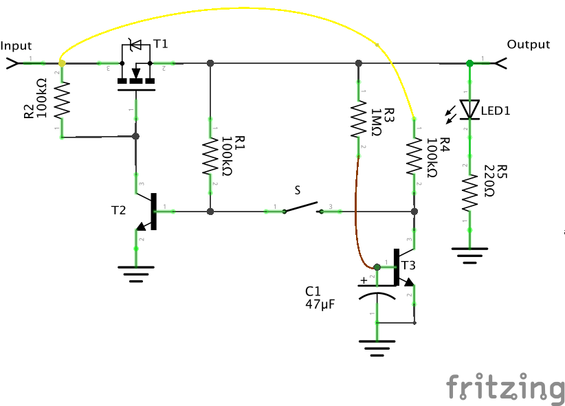
Schematics
We start the redesign by changing transistor T1 from a PNP BJT in the previous circuit to a N-channel FET transistor. While the BJTs can do the job, FETs have better response and are more suitable for use in switching applications. The gate of the FET is tied to the input via resistor R2 to ensure it is not floating and the system stays off when switched off.
The second change is replacing the location of the switch and altering the design so switching is achieved using a single switch. This is done by the addition of transistor T3 to the circuit.
T3 is connected in such a way that when the switch is pressed for the first time, current (through the yellow wire) flows from the input to the base of transistor T2 through the switch(S), turning “on” T2 and creating a conduction path for the gate of T1, effectively turning “on” the system. Current is continuously supplied to the base of T2 through the resistor R1 after the switch is pressed.
The process of turning on the system also gets it ready to be turned off the next time the switch is pressed. As soon as the system is turned “on”, current is supplied to the base of Transistor T3 via resistor R3, turning “on” the transistor which shorts the current from the input (yellow wire) straight to ground. Thus, the next time the switch is pressed, the base of transistor T2 is grounded via the switch, turning “off” T2 which also turns “off” T1, effectively turning off the entire circuit. Because of the speed at which analog circuits responds and the possible slow speed at which the switch will be pressed by a user, a capacitor was used to allow the user enough time on each button press and to also serve as a debouncing mechanism for the switch. A LED is attached at the output to provide visual on/off feedback to the users.
Required Components
With the design ready we can now select the required components for it. While the values of resistors could be varied, it is important the values are sufficiently selected so current draw is enough and are symmetrical to keep the system balanced.
Based on the design, the following components are required;
IRF9110n x1
2n3904 x2
100k Resistor x
Resistor x 1
0ohms Resistor (1)
47uF Capacitor
Led
Jumper Wires
Momentary Pushbutton (1)
For the transistors, I believe you can use any NPN BJT transistor with similar characteristics to the 2n3904 and for the N-Channel FET, the IRF9110 can be replaced with any other similar transistor, just ensure the Vgs of the transistor is compatible with the operating voltage.
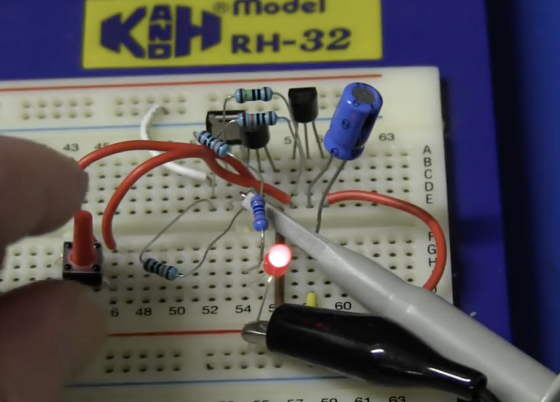
Demo
With the design done, its time to test things out. Connect the components as shown in the main schematics. You should see the LED go on and off in line with the switch press.
Demo
That’s it, this could easily replace mechanical latching toggle switch in your project. Try experimenting with the resistor and capacitor values to observe performance under different conditions.
Feel free to reach out to me via the comment section with questions or general comments on the project.
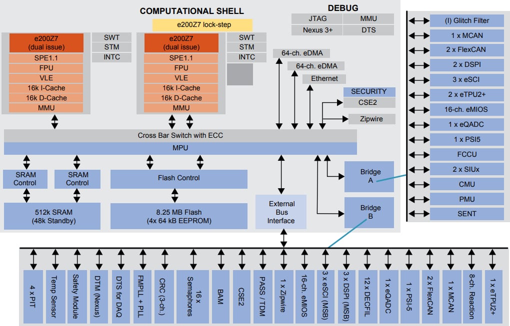
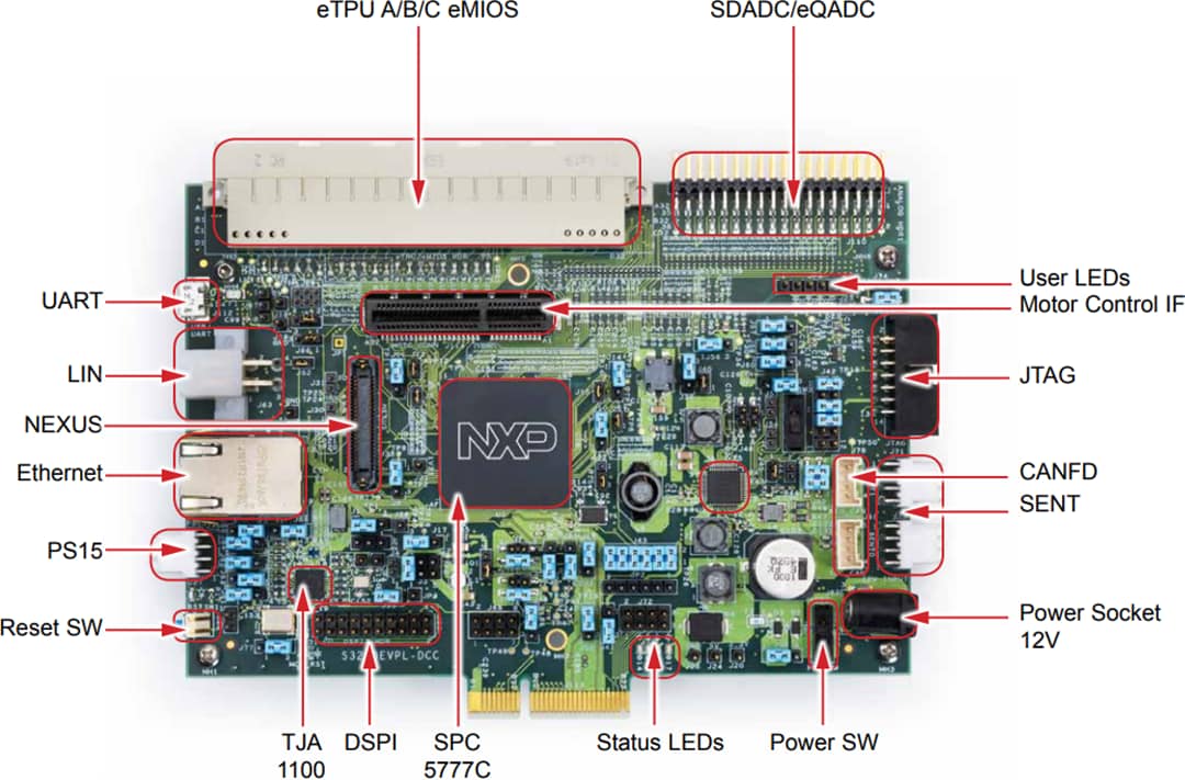
NXP Semiconductors MPC5777C Power Architecture® Microcontroller is a high-performance, multicore MCU optimized for industrial and automotive control applications that require advanced performance, timing systems, security, and functional safety capabilities. The MPC5777C features two independent Power Architecture z7 cores with up to 300MHz operation, along with a single z7 core in Lockstep with one of the main cores. Integrated eTPU timers and Sigma-DeltaADC converters allow for advanced filtering using on-chip knock hardware. On-chip security encryption protection, using CSE and TDM for tamper proofing, help support ASIL-D and SIL-1 functional safety (ISO26262/ IEC61508) requirements.
The MPC5777C Power Architecture® Microcontroller is offered in a Pb-free 416-ball and 516-ball Molded Array Process Ball Grid Array (MAPBGA) package.
Features
Three dual-issue, 32-bit CPU core complexes (e200z7), two of which run in lockstep
Power Architecture embedded specification compliance
Instruction set enhancement allowing variable length encoding (VLE), optional encoding of mixed 16-bit and 32-bit instructions, for code size footprint reduction
On the two computational cores: Signal processing extension (SPE1.1) instruction support for digital signal processing (DSP)
Single-precision floating point operations
On the two computational cores: 16 KB I-Cache and 16 KB D-Cache
Hardware cache coherency between cores
16 hardware semaphores
3-channel CRC module
8MB on-chip flash memory
Supports read during program and erase operations, and multiple blocks allowing EEPROM emulation
512KB on-chip general-purpose SRAM including 64 KB standby RAM
Two multichannel direct memory access controllers (eDMA)
64 channels per eDMA
Dual core Interrupt Controller (INTC)
Dual phase-locked loops (PLLs) with stable clock domain for peripherals and frequency modulation (FM) domain for computational shell
Crossbar Switch architecture for concurrent access to peripherals, flash memory, or RAM from multiple bus masters with End-To-End ECC
External Bus Interface (EBI) for calibration and application use
System Integration Unit (SIU)
Error Injection Module (EIM) and Error Reporting Module (ERM)
Four protected port output (PPO) pins
Boot Assist Module (BAM) supports serial bootload via CAN or SCI
Three second-generation Enhanced Time Processor Units (eTPUs)
32 channels per eTPU
Total of 36KB code RAM
Total of 9KB parameter RAM
Enhanced Modular Input/Output System (eMIOS) supporting 32 unified channels
Two Enhanced Queued Analog-to-Digital Converter (eQADC) modules with:
Two separate analog converters per eQADC module
Support for a total of 70 analog input pins, expandable to 182 inputs with off-chip multiplexers
Interface to twelve hardware Decimation Filters
Enhanced “Tap” command to route any conversion to two separate Decimation Filters
Four independent 16-bit Sigma-Delta ADCs (SDADCs)
10-channel Reaction Module
Ethernet (FEC)
Two PSI5 modules
Two SENT Receiver (SRX) modules supporting 12 channels
Zipwire: SIPI and LFAST modules
Five Deserial Serial Peripheral Interface (DSPI) modules
Five Enhanced Serial Communication Interface (eSCI) modules
Four Controller Area Network (FlexCAN) modules
Two M_CAN modules that support FD
Fault Collection and Control Unit (FCCU)
Clock Monitor Units (CMUs)
Tamper Detection Module (TDM)
Cryptographic Services Engine (CSE)
Complies with Secure Hardware Extension (SHE) Functional Specification Version 1.1 security functions
Includes software selectable enhancement to key usage flag for MAC verification and increase in number of memory slots for security keys
PASS module to support security features
Nexus development interface (NDI) per IEEE-ISTO 5001-2003 standard, with some support for 2010 standard
Device and board test support per Joint Test Action Group (JTAG) IEEE 1149.1 and 1149.7
On-chip voltage regulator controller (VRC) that derives the core logic supply voltage from the high-voltage supply
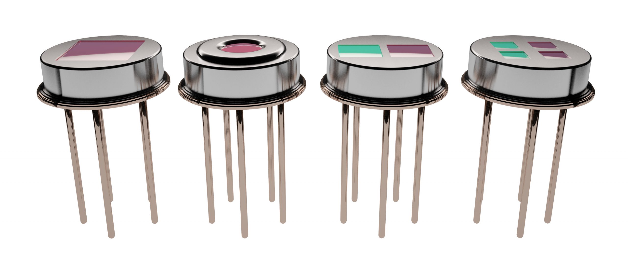
The performance of Pyreos single and dual channel TO-39 detectors in a compact quad channel TO-39 package
Pyreos has announced the launch of a new range of four channel (quad) pyroelectric detectors in TO-39 packaging. These extend the capabilities of the successful Pyreos single and dual TO-39 range, which is used for anaesthesia, refrigerant detection, exhaust gases, carbon monoxide, carbon dioxide and hydrocarbons. The new TO quad devices pack four elements with the proven performance of the Pyreos single and dual channel range and build on the wide range of gases already available.
The new TO-39 quad range benefits from pixel areas five times larger than the previous range and delivers a much higher signal-to-noise (SNR) ratio. The product is mechanically simpler and more robust than competing products as it builds on all the fundamental benefits of the company’s thin-film pyroelectric technology, including simple construction, low vibration sensitivity and thermal stability.
“We’re seeing increasing customer requests for multi-gas detection in a wide range of new applications and have developed this extension of our product range in response,” said Andrew Wallace, CEO at Pyreos. “Using four channels instead of two, we can provide a more efficient multi-gas product for a single, concentrated IR beam. This maximises infrared energy throughput onto the device and reduces sampling error due to spacing. It makes the existing successful technology even more cost-effective for our customers.
Pre-orders are being taken for samples of the new TO-39 quad. Pyreos will be demonstrating its entire product range at the Sensor and Test Show in Nuremberg, 25-27 June 2019, Hall 5 – stand 242.
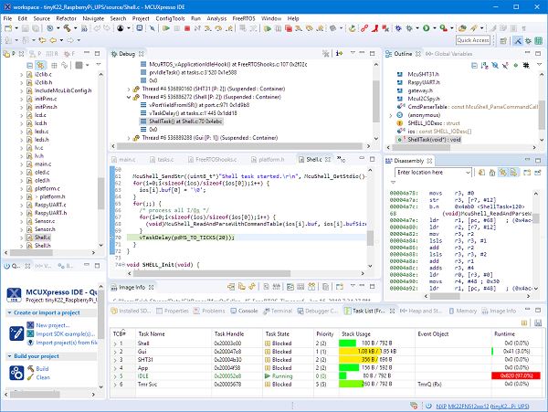
The V11 of the MCUXpresso IDE is again a big step forward: new Eclipse version and 64bit, updated ARM toolchain, extended debugging support for P&E and Segger in addition to the LinkServer connection. The Global Variables view now supports live variables and graphing for P&E and SEGGER in addition to the LinkServer connection. The new views with the Build Analysis, Image Info, Stack usage and Call Analysis are very useful. And for bare metal applications it includes a heap and stack usage view too.
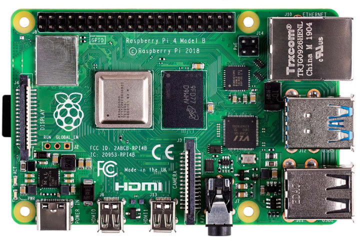
Raspberry Pi has launched Raspberry Pi 4 and it is now on sale, starting at $35. This is a comprehensive upgrade, touching almost every element of the platform. For the first time they provide a PC-like level of performance for most users, while retaining the interfacing capabilities and hackability of the classic Raspberry Pi line.
The new Raspberry Pi 4 B has a much more powerful Broadcom BCM2711quad-core Cortex-A72 processor clocked at up to 1.5 GHz, 1 to 4GB LPDDR4, 4K H.265 video decoding and output support, a proper Gigabit Ethernet port, as well as USB 3.0 and 2.0 ports. Raspberry Pi 4 comes with all those extra features, but the form factor remains the same, and importantly the price is still $35 for the version with 1GB RAM.
In this version of Raspberry Pi there’s a separate Gigabit Ethernet transceiver (BCM54213PE), and USB goes through a VIA VL805 PCIe to 4-port USB 3.0 host controller so the bandwidth is no more shared with USB + Ethernet. They also moved from USB micro-B to USB-C for the power connector. This supports an extra 500mA of current, ensuring it has a full 1.2A for downstream USB devices, even under heavy CPU load.
Wireless Support
Wireless support is provided in an RF shielded module by the same Cypress CYW43455 chip as we saw on the Raspberry Pi 3, Model B+. Offering dual-band 2.4GHz and 5GHz IEEE 802.11.b/g/n/ac wireless networking, as well as Bluetooth 5.0 and Bluetooth LE.
New Raspbian software
According to the Raspberry Pi website:
To support Raspberry Pi 4, we are shipping a radically overhauled operating system, based on the forthcoming Debian 10 Buster release. This brings numerous behind-the-scenes technical improvements, along with an extensively modernised user interface, and updated applications including the Chromium 74 web browser. Simon will take an in-depth look at the changes in tomorrow’s blog post, but for now, here’s a screenshot of it in action.
Some advice for those who are keen to get going with Raspbian Buster right away: we strongly recommend you download a new image, rather than upgrading an existing card. This ensures that you’re starting with a clean, working Buster system. If you really, really want to try upgrading, make a backup first.
Raspberry Pi 4 Model B
Here are the highlights:
A 1.5GHz quad-core 64-bit ARM Cortex-A72 CPU (~3× performance)
1GB, 2GB, or 4GB of LPDDR4 SDRAM
Full-throughput Gigabit Ethernet
Dual-band 802.11ac wireless networking
Bluetooth 5.0
Two USB 3.0 and two USB 2.0 ports
Dual monitor support, at resolutions up to 4K
VideoCore VI graphics, supporting OpenGL ES 3.x
4Kp60 hardware decode of HEVC video
Complete compatibility with earlier Raspberry Pi products
Raspberry Pi 4 specifications:
SoC – Broadcom BCM2711 quad-core Cortex-A72 (ARMv8) @ 1.5GHz with VideoCore VI GPU supporting OpenGL ES 3.0 graphics
System Memory – 1GB, 2GB or 4GB LPDDR4
Storage – microSD card slot
Video Output & Display I/F
2x micro HDMI ports up to 4Kp60 (Currently 1080p60 max. in dual-display configuration, although 2x 4Kp30 is being worked on)
3.5mm AV port with composite video (and stereo audio)
2-lane MIPI DSI display port
Video
Decode – H.265 up to 4Kp60, H.264 up to 1080p60
Encode – H.264 up to 1080p30
Camera – 2-lane MIPI CSI camera port
Audio – Stereo audio via AV port, digital audio via HDMI ports
Connectivity
True Gigabit Ethernet (RJ45)
Dual band (2.4 GHz/5.0 GHz) 802.11b/g/n/ac WiFi 5
Bluetooth 5.0 BLE
USB – 2x USB 3.0 ports, 2x USB 2.0 ports.
Expansion – Standard 40-pin GPIO header fully backward-compatible with previous Raspberry Pi boards
Dimensions – 85 x 56 mm (same as other model B boards)
Temperature Range – 0 – 50°C
Raspberry Pi 4 model B with 1GB RAM sells for the same $35 as the previous model, with the 2GB and 4GB RAM models are coming soon for respectively $45 and $55 with local variations due to taxes, shipping cost, and currency exchange.
Want to see how the new board performs. Check out the benchmarks here.
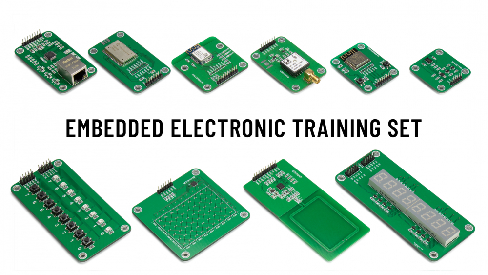
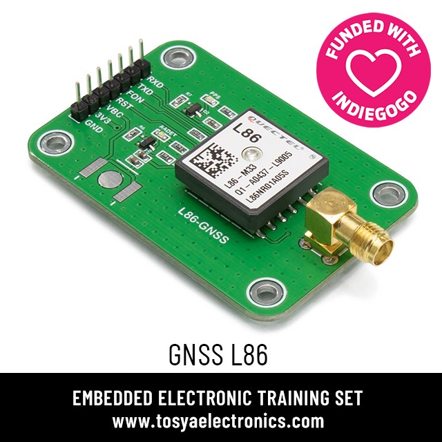
Embedded electronics training set designed for students and developers comprises of an extensive list of modules ready to be used on your next microcontroller project.
Overview
Learn microcontroller programming
Embedded electronics training set designed for students and developers
Students and teens will step into the world of embedded electronics
Prototype designs of our development tools are ready
We will start mass production after the campaign is finished.
Embedded Electronic Training Set consists of seventy-five pieces.
You will buy special products at affordable prices
According to a recent report from Japanese news outlet Nikkei xTech, Sakura Tech Corp has demonstrated a health management system built around its miRadar 8 24GHz-band millimetre wave radar, capable of wirelessly measuring the heart and breathing rates of up to 10 people at the same time. By Julien Happich @ www.eenewseurope.com
Initially designed for automotive and trucking applications such as driver monitoring systems, Sakura Tech’s miRadar 8 unit which measures just 104x76x6mm could also find applications in buildings at room level. The company highlights that its system has a high detection capacity even at night, noting that if a camera were combined with the millimetre wave radar device, the measurement accuracy of the system might be further improved. miRadar 8 can detect obstacles located 30-50m away.
For the purpose of measuring heart and breathing rates with a high accuracy, the maximum detection distance of the system was demonstrated at about 5m, with an azimuth angle range of 45° in the right and left directions. The system comes with two transmission antennas and four reception antennas, all the chips necessary for the radar transmission and reception being integrated into the radar unit.