5900ppi full HD 0.37” LCoS micro-display measures 23.4×8.65mm

AR and VR display manufacturer Raon-Tech has developed a 0.37-inch diagonal full HD (1920×1080) LCoS micro-display (Liquid Crystal on Silicon) aimed at single panel optical display systems such as HMD (Head Mounted Display), HUD (Head-Up Display), and pico projectors. [via www.eenewsled.com]

Embedding an RGB LED driver, a low voltage differential signal receiver and power-down detection circuitry, the RDP370F LCoS micro-display operates at up to 420Hz for sequential colours, in effect supporting 120 RGB frames per second. Gamma corrected resistor string and gamma tab voltages are fully programmable for enhanced gray scaling performance. The display features an array of 1952×1112 pixel designed at a 4.3μm pitch or approximately 5900 ppi. The device draws only 120mW in operation. Together with the display, Raontech also offers a dedicated controller IC, the RDC200, able to perform image processing along with LED control and data formatting for two microdisplays panels simultaneously. The IC includes a special function to correct keystone and compensate optical aberration, enabling developers to design larger FOV devices with the least distortion.

Raon-Tech – www.raon-tech.com

RasPi Arcade Stick – the smart arcade control by TALENTEC

TALENTEC is a Spanish company whose goal is to improve the arcade game experience for players and facilitate this type of entertainment for everyone. To fulfil this premise, they have been working to develop a new concept for the arcade sticks, a smart arcade stick: the RasPi Arcade Stick. In order to check the reception of this product, this company has launched a crowdfunding campaign in kickstarter.

The RasPi Arcade stick is an arcade joystick, with an integrated Raspberry Pi 3 B+. It connects directly to the TV/Monitor vía HDMI and the Raspberry is in charge of making video game emulator. Other features can also be found: a module for SD Card memories and micro USB like power for mobile phones. The processor of this model of Raspberry is an ARM Cortes- A53 that includes wifi ac and Bluetooh 4.2.

Although emulators or the ROMS are not included, it has been tested with RetroPie, Recalbox, Batocera, Lakka and as a media center with Kodi. What’s more, it can be used as a conventional USB arcade stick compatible with PC, PS3 and PS4 in legacy mode.

This gadget will be only sold if the crowdfunding goal is reached and depending on the models and the version, the price is between 54€ and 169€. The project is live on kickstarter and has 12 days to go.

Ultra-small barometric pressure sensor DPS368 from Infineon is Protected against water dust & humidity

Infineon Technologies AG launches the XENSIV TM DPS368. The miniaturized digital barometric pressure sensor is capable of measuring both pressure and temperature. It offers an ultra-high precision of ±2 cm and a low current consumption for precise measurement of altitude, air flow and body movements. This makes the DPS368 ideal for mobile applications and wearable devices offering e.g. activity tracking and navigation. Additionally the sensor can be used in home appliances for airflow control, in drones for flight stability and in medical devices such as smart inhalers.

Due to its robust package, it can withstand 50 m under water for one hour (IPx8) and protects the sensing cells against dust and humidity. As a result, the board handling in an assembly line is also facilitated. The 8-pin LGA package with its small dimensions of 2.0 x 2.5 x 1.1 mm³ saves up to 80 percent space compared to other waterproof sensors.

The pressure sensor element is based on a capacitive sensing principle that guarantees high precision even during temperature changes. The internal signal processor converts the output from the pressure and temperature sensor elements to 24-bit results. Calibration coefficients stored in the sensor are used in the application to convert the measurement results to high accuracy pressure and temperature values. DPS368 provides quick feedback due to a measurement rate of up to 200 Hz and fast read-out speed. The integrated FIFO memory can save up to 32 measurement results, allowing for power-savings on system level.

The XENSIV DPS368 sensor features an average low power consumption of 1.7 μA for pressure measurements at 1 Hz sampling rate. In standby mode, this is reduced to 0.5 μA. The sensor operates at pressure ranges from 300 to 1200 hPa and temperature ranges from -40 to +85 °C with a temperature accuracy of ±0.5 °C. Sensor measurements and calibration coefficients are available through the serial I²C or SPI interface.

The XENSIV DPS368 pressure and temperature sensor can be ordered now. More information is available at www.infineon.com/DPS368.

MIKROE-3512 Fusion for Arm® Development Board

MikroElektronika presents a development board with a debugger over Wi-Fi

The MIKROE-3512 Fusion for Armv8 development board from MikroElektronika is designed for rapid development of embedded applications. Redesigned from the ground up, it offers broad set of standards as well as several unique features never seen before in the world of embedded electronics: programming and debugging over Wi-Fi network, support for many different Arm Cortex®-M based microcontrollers regardless of their pin number, and more.

The development board is designed so that the developer has everything that might be needed, following the Swiss Army knife concept: a highly advanced programmer/debugger module, a powerful and clean power supply module, a huge set of connectivity options including USB, Ethernet, CAN (on the MCU Card, if supported), and UART, as well as a set of MikroE proprietary standards and technologies, including the well-established mikroBUS™ standard, a standardized MCU card socket, and a standardized 2 x 20 display connector. Several interactive options are also available including buttons, LEDs, switches, and more. All these features are packed on a single development board, which itself uses innovative manufacturing technologies, delivering fluid and immersive working experience.

The powerful CODEGRIP module, an Arm Cortex-M compatible programmer/debugger, supports a wide range of different Arm Cortex-M based MCUs produced by several major chip vendors. It allows in-place programming and debugging of all supported microcontrollers, offering many options including the support for JTAG, SWD and SWO Trace (single wire output), seamless integration with the MikroE software environment, and some powerful and unique features such as the programming/debugging over Wi-Fi. Fusion for the Armv8 development board is also an integral part of the MikroE rapid development ecosystem. Natively supported by the MikroE software toolchain and backed up by hundreds of different Click board™ designs with their number growing on a daily basis, it covers many different prototyping and development needs, saving precious development time.

The board is available for purchase from various distributors online for ~ $457.98.

TI introduces a new ultra-high-speed analog-to-digital converter

ADC12DJ5200RF promises the fastest sampling rate and lowest power consumption. via www.eenewsembedded.com

At 8 GHz, the ADC12DJ5200RF enables engineers to achieve as much as 20 percent higher analog input bandwidth than competing devices, which gives engineers the ability to directly digitize very high frequencies without the power consumption, cost and size of additional down-conversion.

In dual-channel mode, the ADC12DJ5200RF samples at 5.2 gigasamples per second (GSPS) and captures instantaneous bandwidth (IBW) as high as 2.6 GHz at 12-bit resolution. In single-channel mode, the new ultra-high-speed ADC samples at 10.4 GSPS and captures IBW up to 5.2 GHz.

The ultra-high-speed ADC greatly minimizes system errors with offset error as low as ±300 µV and zero temperature drift.

The ADC12DJ5200RF will achieve high measurement accuracy for 5G testing applications and oscilloscopes, and direct X-band sampling for radar applications.

For more information, see www.ti.com/ADC12DJ5200RF-pr

Sony’s ELTRES LPWAN Module Promises a Range of over 100 Km

Contributing to delivery of wireless communication services that are stable over long distances and while moving at high speeds.

Tokyo, Japan—Sony Corporation today announced the upcoming release of the CXM1501GR communication module, which is compatible with the ELTRES™ low-power wide area (LPWA) wireless communication standard that Sony has developed for IoT applications. Equipping IoT devices with this communication module enables them to connect to the ELTRES™ IoT Network Service, which is scheduled to begin service rollout this coming autumn from Sony Network Communications Inc.

Sony is positioning this product for application in a broad range of IoT devices, aiming to develop various services making the most of stable wireless communications over long distances and while moving at high speeds, thereby creating a new market.

Most IoT systems wirelessly transfer information obtained by various sensors to cloud servers, where the data is collected and processed, and the output then sent to user devices such as smartphones or tablets for display. An LPWA network is a low-power wireless telecommunication technology used for transferring low-bit data across a wide area, and it is expected to see significantly growing demand for communication in IoT systems.

The new CXM1501GR communication module integrates a newly developed transmitter LSI that transmits signals conforming to the protocol of the ELTRES™ wireless communication standard in the 920MHz band as well as a circuit for impedance matching with an externally mounted antenna. Also included are a GNSS receiver LSI—an important IoT sensor that obtains time and position information—and high-frequency components such as the SAW filter required for the GNSS receiver. With all of these components built in, this product expands the ease and versatility of IoT edge device design.

Main Features

  1. Built-in π/2-shift BPSK modulation (biphasic deviation modulation) LSI that operates on low power and produces a favorable SN ratio in narrow bandwidth communication.
  2. Built-in impedance-matching circuit for 920MHz external antenna allows for direct connection to a general-purpose antenna and enables custom antenna to be designed easily.
  3. Built-in high-sensitivity, low-power GNSS LSI for compatibility with GPS, GLONASS, and QZSS.
  4. Built-in high-frequency circuit optimized for GNSS reception enabling direct connection to antennas.
  5. Has obtained certification for wireless communication equipment construction and design in compliance with the Radio Act of Japan(Certification number: 007-AG0043); No further certification required when the listed antenna are used.
  6. Has obtained module type-certification from the Japan Approvals Institute for Telecommunications Equipment as compliant to Japan’s Telecommunications Business Act.

CXM1501GR diagram and system configuration sample

more information on: www.sony.net

Samsung’s Two New USB PD Controllers support up to 100W-charging

SE8A is the first power delivery controller with embedded Secure Element for added protection against unauthorized chargers The new chips support up to 100W-charging and meets latest USB-PD 3.0 specifications.

Samsung Electronics, a world leader in advanced semiconductor technology, today announced two USB Type-C power delivery (PD) controllers, SE8A and MM101. With the new PD controllers, power chargers are able to communicate with the device to deliver the optimum amount of power for more efficient charging through authorized products.

Both chips are built with an embedded Flash (eFlash) that allows the flexibility of modifying its firmware to meet the most up-to-date specifications and are able to supply up to 100 watts (W, 20V / 5A). SE8A is the first PD controller in the industry to embed Secure Element, adding an extra layer of security to PD controllers.

The new PD controllers meet the most recent USB specifications for fast-charging, USB-PD 3.0, that addresses the compatibility and efficiency challenges across different mobile devices as well as other electronics. Such challenges can cause the device to charge slower than usual or excessively than required that can also compromise the lifecycle of the battery. With the growing need to extend always-on experiences quickly and as more devices adopt USB interfaces for charging and data transmission, efficient and secure fast-charging technologies are expected to benefit consumers through a wide range of applications.

“In addition to smarter features and larger batteries, innovative charging solutions allow us to do more through our mobile devices today. Following this trend, power adapters that can quickly charge devices while establishing safeguards against unauthorized access are increasingly in demand,” said Ben K. Hur, senior vice president of System LSI marketing at Samsung Electronics. “Samsung’s power delivery MM101 and security-enhanced SE8A will not only make charging faster and safer but also enable new services that can enrich tomorrow’s mobile experiences.”

The MM101 supports a symmetric encryption algorithm, Advanced Encryption Standard (AES), for product authentication and includes moisture sensing capabilities to ensure safer charging conditions.

Samsung’s SE8A is the industry’s first solution that combines a PD controller and Secure Element (CC EAL5+ equivalent) in a single chip, providing extra measures of protection such as security key storage, and encoding and decoding of sensitive data within a device in a compact form factor. The SE8A supports USB Type-C Authentication, a certificate-based authentication program for USB Type-C chargers and devices that prevents the misuse of unapproved products. With enhanced security, the SE8A opens possibilities for new kinds of content and services that may be exclusive to a certain brand, location or event.

By supporting up to a 100W capacity, compared to the general smartphone charger’s 10W, power chargers with Samsung’s PD controllers can be used for a variety of devices other than smartphones such as tablets, laptops and monitors.

For additional safety, both chips also provide over-voltage protection. The MM101 is currently sampling and the SE8A is in mass production.

Sensirion – Evaluation Kit for Environmental Sensors with New Modular Approach

Sensirion, the expert in environmental sensing, relaunches the evaluation kit SEK-Environmental Sensing with a new modular approach. The SEK-Environmental Sensing allows engineers to evaluate sensors and develop innovative sensor applications even more quickly and easily. The kit combines plug-and-play hardware with an easy-to-use viewer software, the ControlCenter, enabling in-depth evaluation of all Sensirion environmental sensors.

Each evaluation kit can be customized individually now. Get a SEK-SensorBridge, choose your SEK-Evaluation-Sensors, download Sensirion’s SEK-ControlCenter viewer software and start evaluating. The SEK-SensorBridge features two independent I2C channels that allow simultaneous evaluation of two environmental sensor samples. The SEK-ControlCenter viewer software makes it possible to display and log the sensor signals for multiple sensors connected to several SensorBridges on the same PC.

Visit our website and customize your Sensirion evaluation kit now: www.sensirion.com/sek

Learn more about environmental sensing and our sensor solutions on: www.sensirion.com/environmental-sensing

Intel launches first 10th Gen Ice Lake CPUs with 10nm fabrication

A photo released May 28, 2019, at Computex 2019 shows the 10th Gen Intel Core processor. 10th Gen Intel desktop processors unveiled at Computex enable fast, immersive experiences with up to 4 cores and 8 threads, up to 4.1 GHz max turbo frequency and up to 1.1 GHz graphics frequency. (Source: Intel Corporation)

10th Gen Intel Core Processors: Highly Integrated; Broad-Scale AI to the PC

Intel announced the first 10th Gen Intel Core processors, bringing high-performance AI to the PC at scale with Intel® Deep Learning Boost (Intel DL Boost). The processors are built on the company’s 10nm process technology, new “Sunny Cove” core architecture and new Gen11 graphics engine. 10th Gen Intel Core processors will range from Intel Core i3 to Intel Core i7, with up to 4 cores and 8 threads, up to 4.1 max turbo frequency and up to 1.1 GHz graphics frequency.

A photo released May 28, 2019, at Computex 2019 shows a 10th Gen Intel Core processor wafer. 10th Gen Intel desktop processors unveiled at Computex enable fast, immersive experiences with up to 4 cores and 8 threads, up to 4.1 GHz max turbo frequency and up to 1.1 GHz graphics frequency. (Source: Intel Corporation)

10th Gen Intel Core processors will take thin-and-light laptops and 2 in 1s to the next level, offering:

  • Intelligent performance: Intel’s first processors designed to enable high-performance AI on the laptop, delivering approximately 2.5x AI performance1 with Intel DL Boost for low latency workloads. The new graphics architecture delivers up to 1 teraflop of vector compute for heavy duty inference workloads to enhance creativity, productivity and entertainment on highly mobile, thin-and-light laptops. For low-power AI usages on the PC, Intel® Gaussian Network Accelerator (GNA) is built into the SoC.
  • A leap in graphics capabilities: New Intel Iris Plus graphics, based on the Gen11 graphics architecture, nearly doubles performance2 for stunning visual experiences. Reach pro-level content creation capabilities on the go with approximately 2x HEVC encode4; watch 4K HDR in a billion colors5; game with up to 2x faster FPS6 and play thousands of popular titles in 1080p.
  • Best-in-class connectivity: Delivering both integrated Thunderbolt™ 3 and integrated Intel® Wi-Fi 6 (Gig+) for the first time to enable nearly 3x faster wireless speeds3 alongside the fastest7 and most versatile port available. Intel’s Gig+ implementation of Wi-Fi 6 connectivity delivers greater than 1 Gbps wireless speeds8 with enhanced reliability and performance.
Intel unveils its 10th Gen Intel Core desktop processors on May 28, 2019, at Computex 2019 in Taipei, Taiwan. 10th Gen Intel desktop processors unveiled at the event are based on Intel’s 10nm technology and are now shipping. (Credit: Intel Corporation)

Intel’s highly integrated 10th Gen Intel Core processors give OEM partners the freedom to innovate on design and aesthetic by reducing the silicon footprint while still delivering the latest and greatest standards and world-class performance. The new 10th Gen Intel Core processors are now shipping, with OEM systems expected to be available for holiday 2019.

Intrinsyc Announces Open-Q™ 212A SOM and Development Kit based on the Qualcomm® Home Hub 300 Platform

Designed for next-gen home hub products requiring advanced audio and multi-mode wireless capabilities, including Wi-Fi, Bluetooth, BLE, and Zigbee.

Intrinsyc Technologies Corporation, a leading provider of solutions for the development and production of embedded and Internet of Things (IoT) products, today announced the availability of the Open-Q™ 212A system on module (“SOM”) and Home Hub Development Kit.

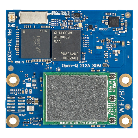
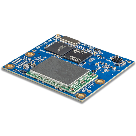
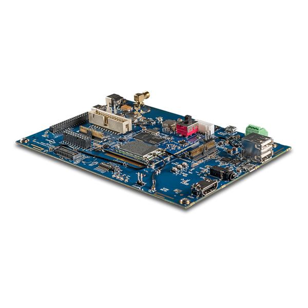
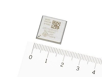
Intrinsyc’s Open-Q™ 212A SOM is a compact (50mm x 46.5mm) pre-certified, production-ready embedded computing module that is ideal for cost-sensitive home hub, home automation, and smart audio devices featuring voice control, AI, and wireless connectivity. It is powered by the Qualcomm® Home Hub 300 Platform based on the Qualcomm® APQ8009 System-on-Chip (“SoC”) and includes an advanced Qualcomm audio and voice optimization solution supporting multi-mic beamforming and noise cancellation as well as Hi-Fi stereo audio playback. The 212A SOM satisfies wireless connectivity needs of home hub/home automation devices with a high throughput, pre-certified, Wi-Fi/BT module, supporting dual-band 802.11ac 2×2 MU-MIMO as well as concurrent Bluetooth with independent Wi-Fi and Bluetooth antenna ports for optimal coexistence performance.

“Intrinsyc’s Open-Q™ 212A SOM brings high performance wireless connectivity and advanced audio capability to a variety of voice-controlled smart home applications,” said Clifford Morton, Vice President, Client Solutions, Intrinsyc. “OEMs can quickly develop products and applications using Intrinsyc’s Linux based development platform and their choice of voice services SDKs available from leading vendors. When development is complete OEMs can immediately go into production with Intrinsyc’s Open-Q™ pre-certified system on module.”

Additional information on the Open-Q 212A SOM is available at:

https://www.intrinsyc.com/computing-platforms/open-q-212A-som/

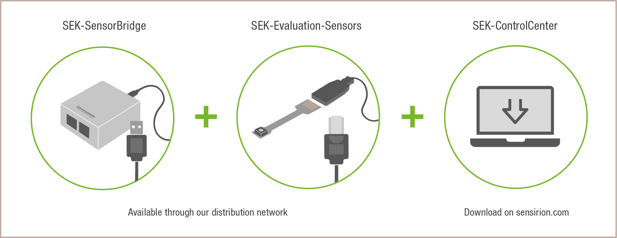
To help IoT device developers quickly evaluate the 212A SOM and jump-start new product development, Intrinsyc offers a full-featured development platform to support the SOM. The 212A Home Hub Development Kit provides a SOM, carrier board, and power supply; everything needed to start your product development today – the carrier board provides audio peripherals to support voice controlled and smart speaker applications, extensive I/O expansion connectors, Wi-Fi and Bluetooth antennas, and multiple USB ports. To support even more wireless connectivity options, including Zigbee, 802.15.4, and Bluetooth LE 5.0, the Dev Kit will support the Qualcomm® QCA4024 SoC add-on board. This optional accessory board plugs into the Open-Q 212A Dev Kit and features a Qualcomm QCA4024 module along with all supporting connections to the 212A SOM. The QCA4024 board is in the final stages of development and will be available in late June, 2019.

The Development Kit is available for purchase at:

https://shop.intrinsyc.com/products/open-q-212a-development-kit

The Home Hub Dev Kit comes pre-loaded with an OpenEmbedded Yocto Linux OS, initially with support for audio and wireless connectivity features, such as Wi-Fi station and AP modes, BT speaker, BT LE, stereo speaker outputs, and the microphone array with Qualcomm voice and audio optimization for advanced beamforming and noise cancellation. Further SW updates will be coming soon to support the QCA4024 wireless expansion board, as well as other features and demo applications including – home automation gateway, voice activation, and voice services SDKs.

Open-Q™ 212A SOM Specifications:

  • Qualcomm® APQ8009 SoC with Quad-Core ARM Cortex A7 (32-bit) 1.267GHz
  • Qualcomm® Adreno™ 304 GPU and QDSP6 DSP
  • 1GB LPDDR3 RAM, 4GB eMMC Flash storage
  • Pre-certified Wi-Fi/BT – 802.11a/b/g/n/ac, 2×2 MU-MIMO, 2.4/5Ghz, Bluetooth 4.2
  • Display interface: 4-lane MIPI DSI interface for LCD up to 720p
  • Camera interface: Up to 8MP over 4-lane MIPI CSI interface
  • Qualcomm Aqstic™ audio codec on SOM (WCD9326).

Open-Q™ 212A Home Hub Dev Kit Features:

  • Advanced audio on dev kit:
    • Hi-Fi audio codec on SOM
    • Stereo speaker amps on carrier board
    • Multi-mic array on carrier board
    • Audio expansion interfaces for other audio peripherals
  • Separate Wi-Fi and Bluetooth antennas on carrier board
  • Support for optional QCA4024 Zigbee/BLE add-on board (coming)
  • Camera connector for optional camera accessory
  • OpenEmbedded Yocto Linux OS.

To aid OEMs with rapid product development, Intrinsyc provides full documentation, access to SW source code, technical support, as well as turnkey product development services, driver and application software development, and custom hardware design.

Contact Intrinsyc at sales@intrinsyc.com with your product requirements and have one of the Company’s solution architects help plan for your successful product development and launch.

TOP PCB Companies