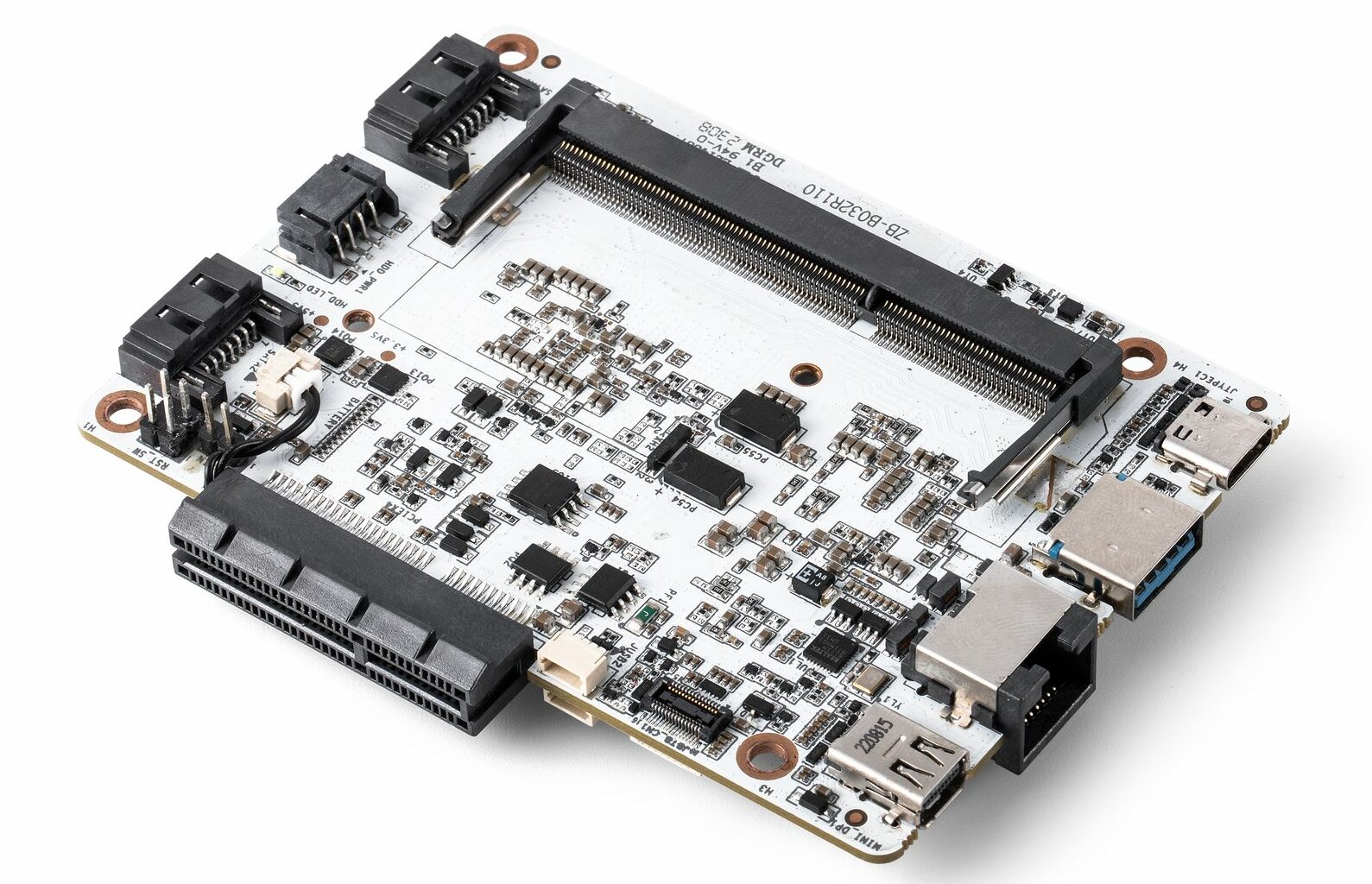
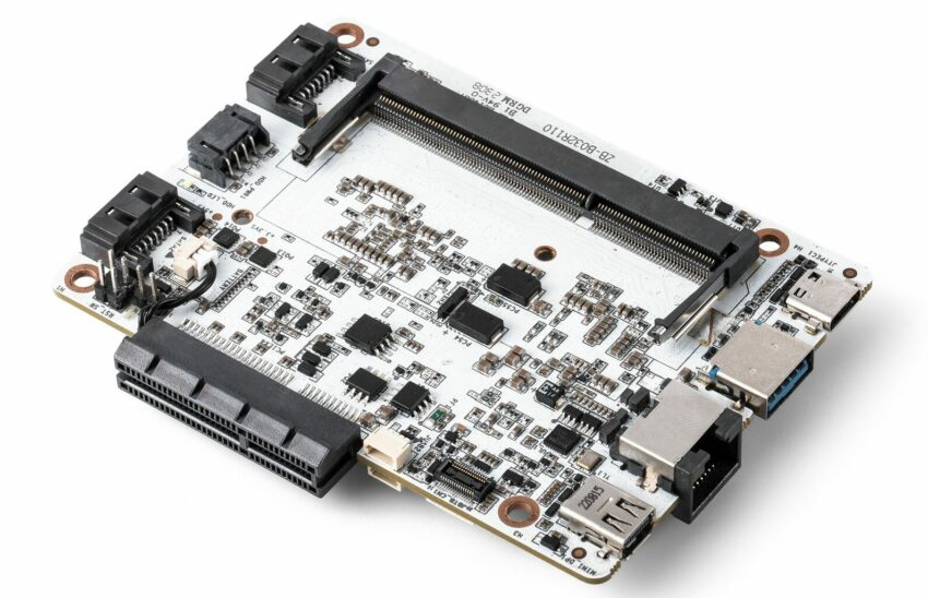
IceWhale Technology has launched the ZimaBlade, a single-board computer with mediastreaming, retro gaming, and personal server capabilities. Equipped with an Intel Celeron Quad-core processor, this device offers PCIe support, dual SATA connectors, Gigabit Ethernet, and runs on Open-Source CasaOS. Priced at US$64, IceWhale Technology hopes to begin shipping the product at the end of January 2024.
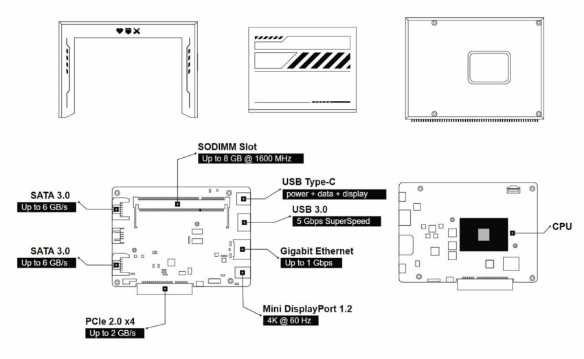
Talking about features and specifications, this board has a lot to offer; it supports 16GB of DDR4 RAM with a 32GB of internal EMMC storage option. It has PCIe slots, SATA ports, and USB ports for expansion, and it has a MiniDP 1.2 interface, a DisplayPort over USB-C, and a board-to-board eDP interface, all supporting 4K@60Hz resolution.
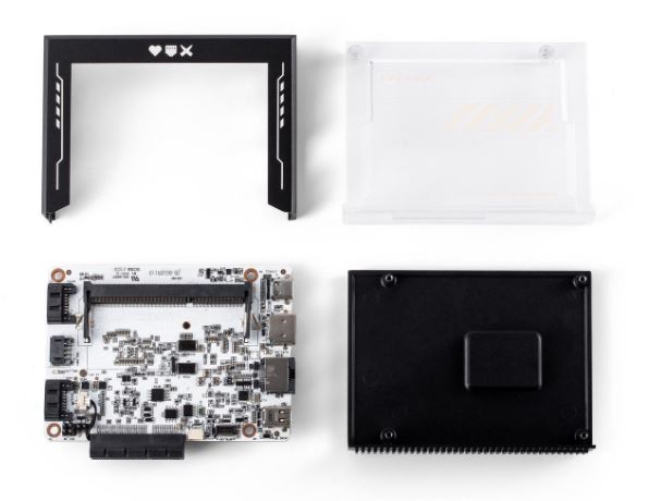
The product page also mentions a three-piece enclosure that keeps ZimaBlade protected and stylish. The enclosure is designed in three parts. The bottom part is made with aluminum, which is thermally coupled to the mainboard’s processor to dissipate heat for silent, fan-free operation. The frame and the top plate are made with injection-molded polycarbonate to give the whole product a dazzling look.
If you are trying to get a NAS up and running with this device, the process is straightforward, and you can do that instantly. On top of that, it supports up to 154 TB of storage you can access. The device also efficiently handles auto GPT operations and offers a delightful experience for retro gaming enthusiasts.
Graphics: Up to 700 MHz, Intel® Quick Sync Video, Intel® Clear Video HD Technology, Intel® Clear Video Technology
PCIe: 1 x PCIe 2.0, four lanes
USB: 1 x USB Type-C (data + power + display), 1 x USB 3.0, 2 x USB 2.0
Power: 45 W USB Type-C power adapter
Thermal: 6 W TDP with passive cooling
Dimensions: 107 mm x 80 mm x 23 mm
Enclosure: Custom injection molded polycarbonate (opaque and transparent), aluminum alloy heatsink, four black silicone feet
Software: Pre-installed Debian-based CasaOS with a streamlined Docker experience. Compatible with Windows, Ubuntu, Debian, Raspberry Pi OS, CentOS, OpenWrt, pfSense, Android, LibreELEC, and more.
IceWhale has started making a few ZimaBlade computers to test them out. They plan to make many more in October and send them to supporters by January 2024.
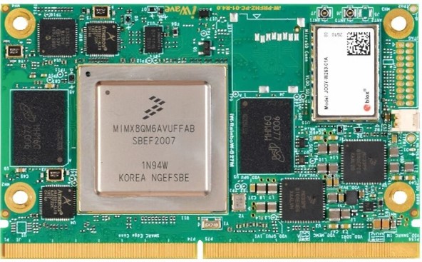
The i.MX 8 family applications processor supports advanced media processing, secure domain partitioning, and vision processing, making it ideal for applications such as automotive infotainment, advanced industrial HMI & control, home automation, and many more.
Advantages of i.MX 8 series include:
Easily combine multiple systems into one
Build diverse platforms with multiple operating systems on a single i.MX 8 processor
Create independent GPU displays and functionalities by partitioning the resources
Implement end-to-end security solutions
Multi-display & multi-domain functionality
Develop up to 4x 1080p screen with independent content
Dual-core Cortex-M4F for offloading real-time tasks
Highly scalable platform to enable seamless machine interfaces
Multi-domain voice recognition and audio processing
Build advanced vision-based HMI systems
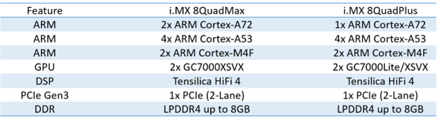
Build multimedia platforms with i.MX 8QuadMax/QuadPlus System on Modules
As processing capabilities increase, so do the complexity and scope of developing embedded systems.
iWave introduces i.MX 8QuadMax/QuadPlus System on Module offloading several complexities involved in the design cycle. The SoM combines high-performance computing with industry-leading video and audio capabilities.
Key features include:
High-performance computing at low power
Single, dual, or quad-core Cortex-A53 cores running at up to 1.2GHz
Dual Cortex-A72 core up to 1.6GHz
Heterogeneous multicore processing with Cortex-M4F running at up to 264 MHZ for advanced system control
World-class multimedia performance
Up to 4Kp60 H.265 video decoding
Up to 4Kp30 H.264 decode capable VPU
1080p30 H.264 encode capable VPU
High-performance 3D graphics processing unit
Enhanced Vision Capabilities (via GP)
Highest levels of pro audio fidelity using SAI/I2S – Audio Interface
Support for high-speed interfaces
Gigabit Ethernet, USB3.0, SATA3.0, and multiple GPIO interfaces
High-speed PCIe v3.0 interface support
Display – HDMI2.0 (up to 4K), LVDS, MIPI-DSI (up to 4 Lanes) (720p @60fps)
Enabling vision using 2 x MIPI-CSI (up to 4 Lanes)
Support 1080p30, 720p60, VGA at 60 fps
Enable sophisticated security features
Secure Boot, Secure storage, Wi-Fi Security, and OPTEE
Extensive BSP support
Linux 5.10.52
Ubuntu 20.04 LTS
Android Pie 11.0.0
QNX 7.0.0 (or higher)
Table 1.0: Differentiating features of i.MX 8 System on Module
Wireless connectivity with iWave i.MX 8 SoM
Adding to its exceptional capabilities to support multimedia platforms, the i.MX 8 SoM comes integrated with u-Blox JODY-W3 making it compatible to support Wi-Fi 6 (802.11ax) and Bluetooth 5.1.
Each Wi-Fi 6 access point covers a larger area and can support more devices simultaneously. Wi-Fi 6 also provides a significant speed boost, as well as 50% increase in battery life, a 4x increase in network capacity, and a 2x increase in bandwidth over previous generations of Wi-Fi.
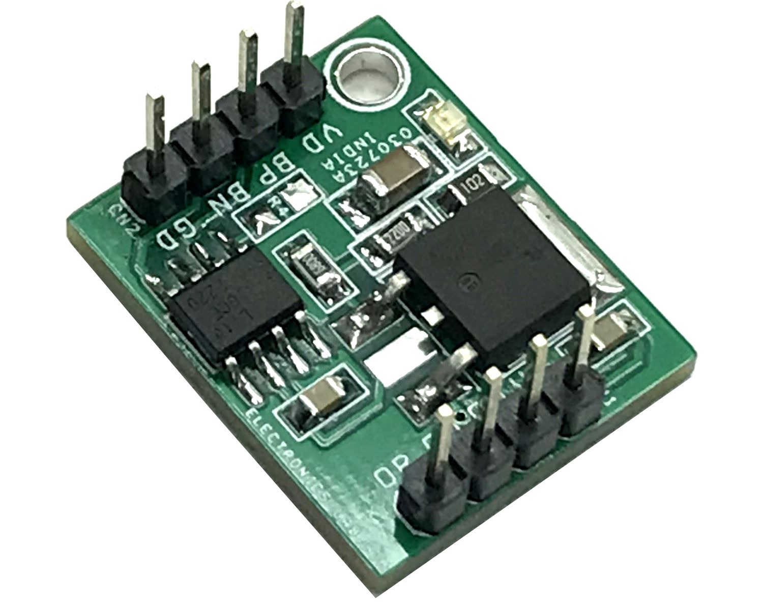
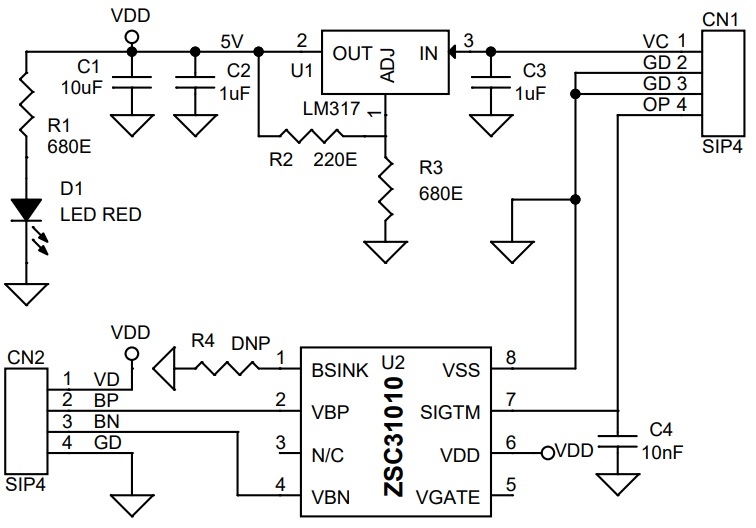
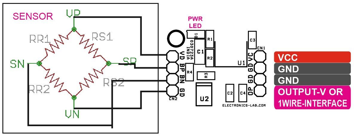
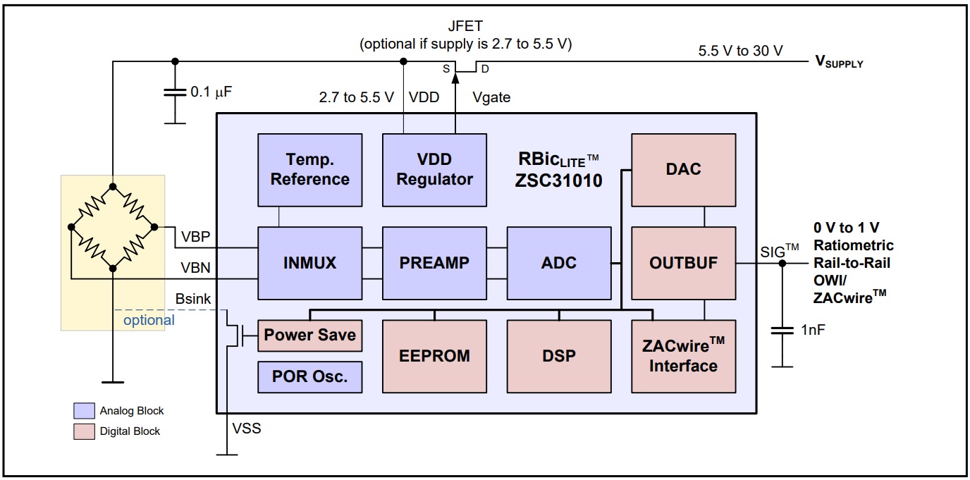
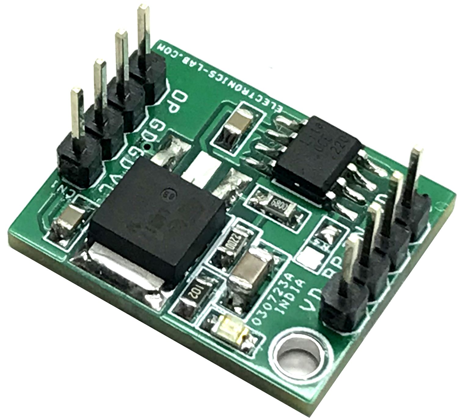
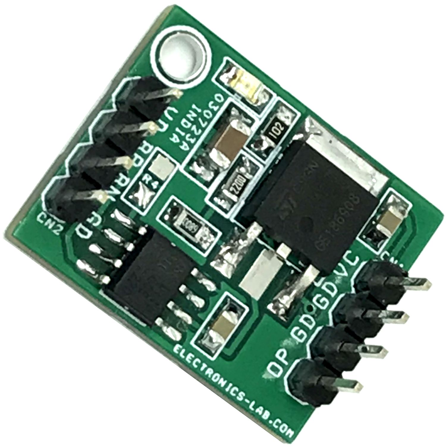
The module presented here is a sensor signal conditioner based on ZSC31010 CMOS integrated circuit, which enables easy and precise calibration of resistive bridge sensors via EEPROM programming. When mated to a resistive bridge sensor, it will digitally calibrate offset and gain with the option to calibrate offset and gain coefficients and linearity over temperature. A second-order compensation can be enabled for temperature coefficients of gain or offset or bridge linearity. ZSC31010 module communicates via IDT’s ZACwire serial interface to the host computer and it is easily mass-calibrated in a Windows environment. Once calibrated, the output signal pin can provide selectable 0 to 1 V absolute analog output; rail-to-rail ratiometric analog output; or digital serial output of bridge data with optional temperature data. U1 LM317 provides the 5V DC to the sensor chip. D1 is the power LED.
Note: This sensor module requires a simple PC-controlled configuration and calibration via ZACwire™ One-Wire Interface.
Click the link below to download the calibration software, more information about the ZSC31010, and a video tutorial about the ZACwire interface.
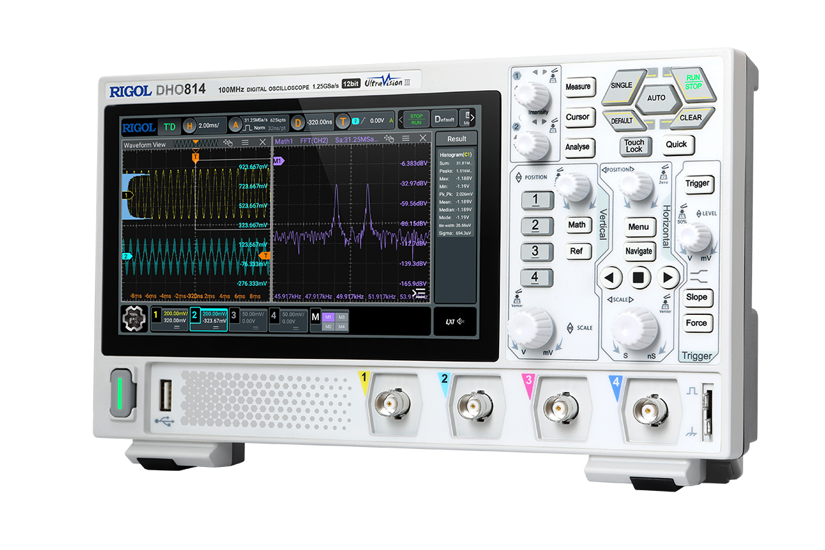
Rigol’s newest high-performance 12 bit economical digital oscilloscopes are not only very portable but they offer high-resolution based on Rigol’s “Centaurus” technology platform, a capture rate up to 1,000,000 wfms/s, up to 50 Mpts memory depth, with an ultra-low noise floor that allows the detection of even small signal details.
Saelig Company, Inc. has introduced the Rigol DHO800/900 Oscilloscope Series, Rigol’s newest high-performance 12-bit economical digital oscilloscopes. Not only are they very portable, but they offer the high-resolution needed today, based on Rigol’s “Centaurus” technology platform. With a capture rate up to 1,000,000 wfms/s (in UltraAcquire Mode), and 25/50Mpts memory depth, the ultra-low noise floor of these scopes allows the detection of even small signal details.
Additionally, the DHO900 series supports 16 digital channel capture, allowing analysis of both analog and digital signals simultaneously to meet complex embedded design and test tasks. Affordably priced, these scopes provide auto serial and parallel bus analysis, Bode plot analysis, and many other functions needed for today’s test demands in R&D, education, and scientific research.
DHO800 Series Highlights
Ultra-low noise floor, pure signal depiction, captures small signals
Up to 12-bit resolution for all the models
Analog bandwidth of 70MHz & 100 MHz, 2 & 4 analog channels
Max. real-time sample rate 1.25GSa/s
Max. memory depth 25Mpts
Vertical sensitivity range: 500uV/div to 10 V/div
Max. capture rate of 1,000,000 wfms/s (in UltraAcquire mode)
Digital phosphor display with real-time 256-level intensity grading
Waveform search and navigation function
7″ (1024×600) capacitive multi-touch screen
New user-friendly Flex Knob control
USB Device & Host, LAN, and HDMI interfaces (std.) allows remote control
Additional DHO900 Series Highlights
16 digital channels (std. but logic probe purchase is required)
Max. real-time sample rate of 1.25GSa/s
Max. memory depth 50Mpts
Vertical sensitivity range: 200uV/div to 10 V/div
Rigol DHO800/900 Oscilloscopes are available now from Saelig Company, Inc., Rigol’s USA technical distributor.
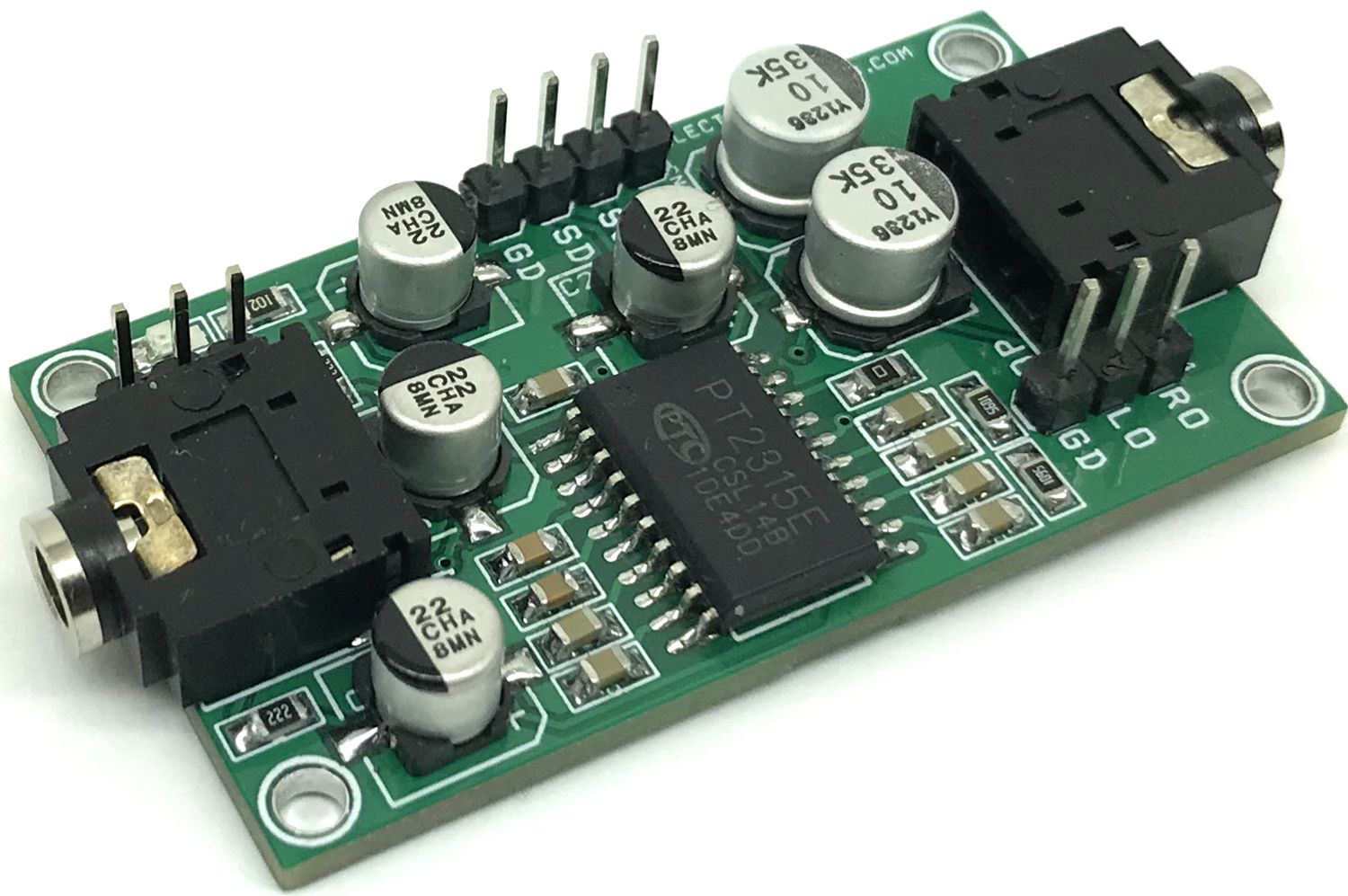
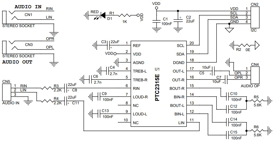
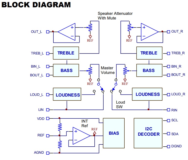
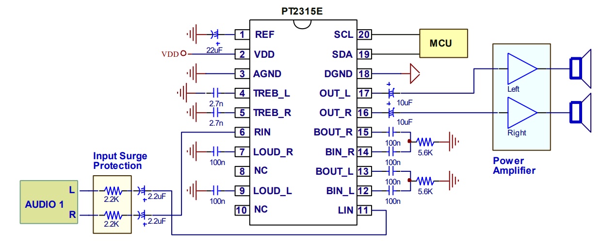
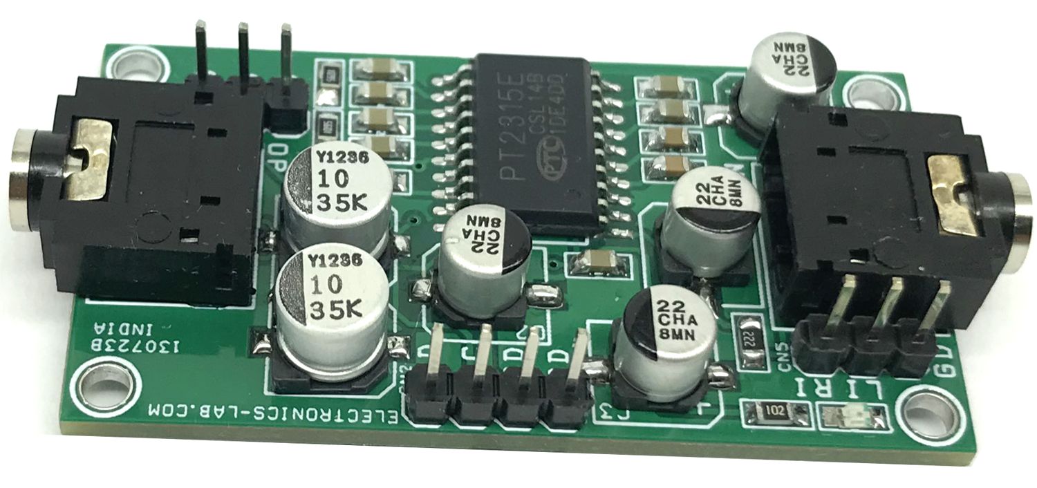
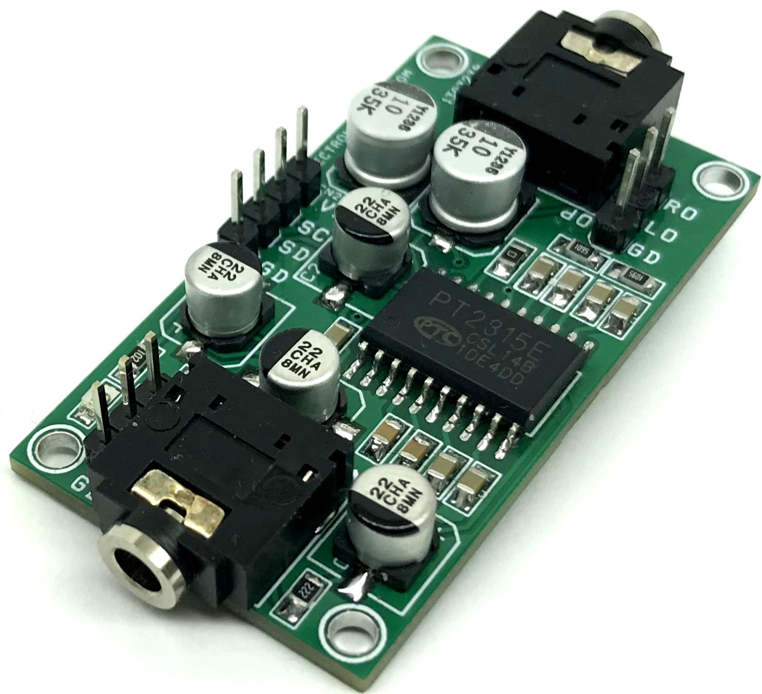
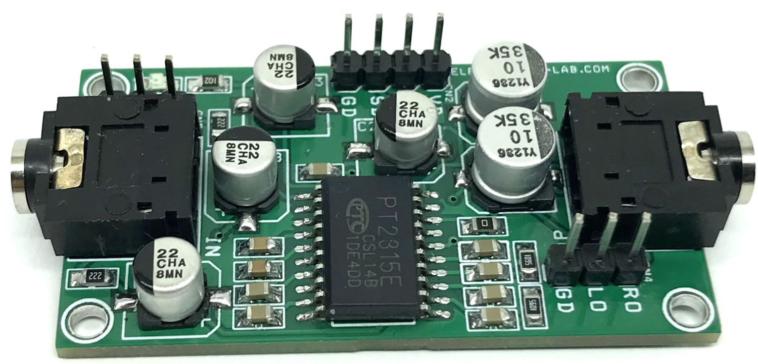
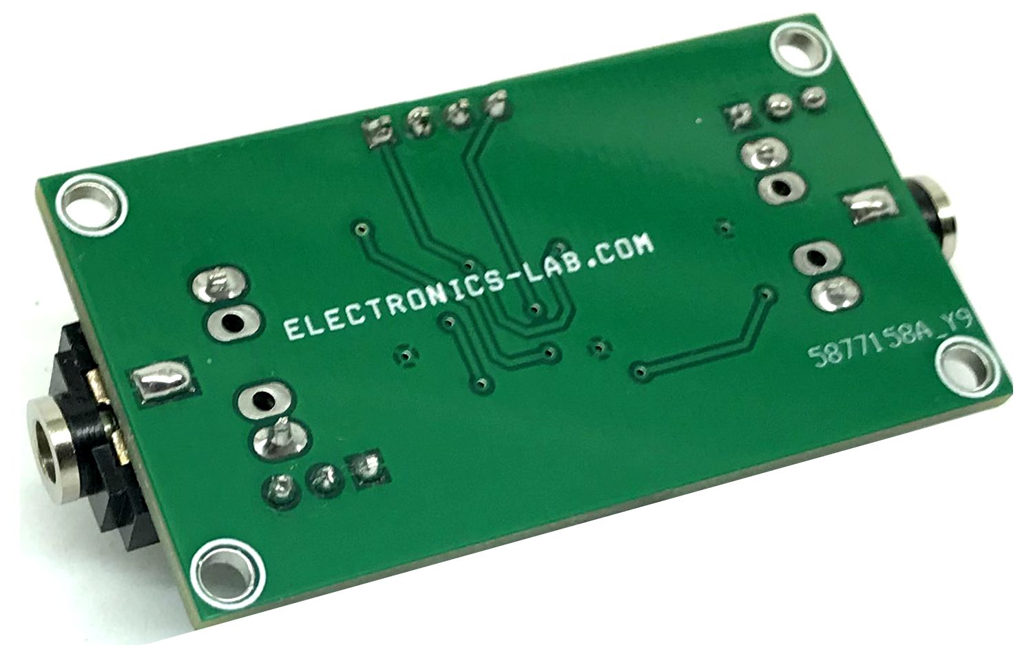
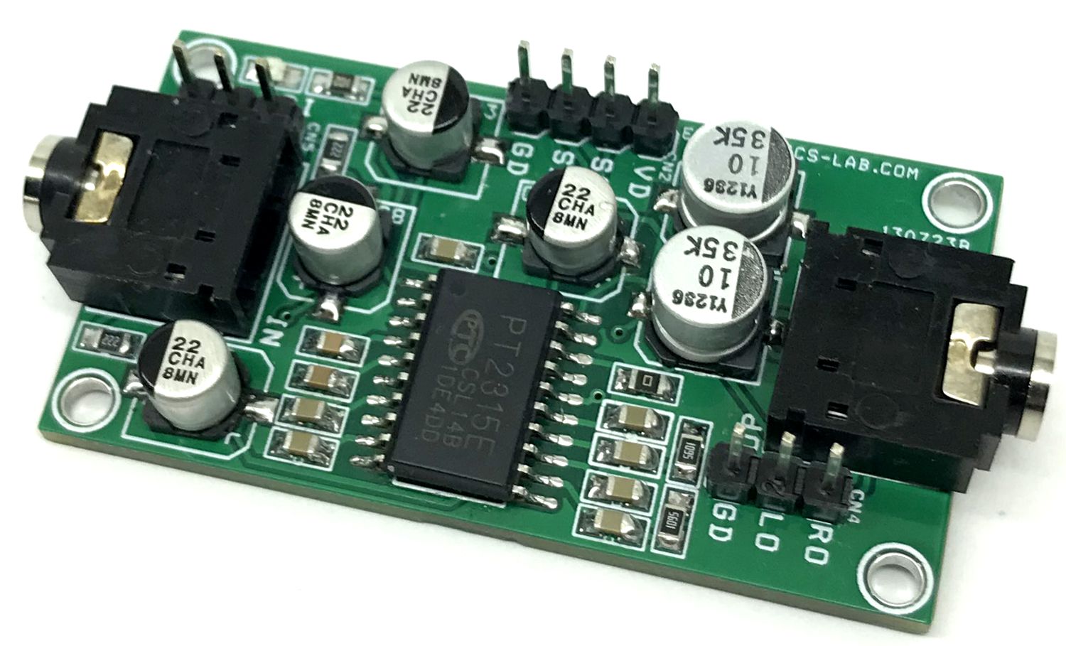
This PT2315E IC-based audio processor is designed for versatile applications and includes master volume control with low-frequency loudness compensation, speaker output attenuator, and tone control. It is a good solution for home audio signal processing. Due to the high-reliability requirement from the audio business, the PT2315E improves both audio performances and input surge current capability and these cause the PT2315E to be the best solution for the cost-effective audio systems.
Features
Power Supply 5V DC (Range 4V to 10V)
Master volume from 0 dB to -78.75dB in 1.25dB/step
Speaker attenuator for balance ranges from 0dB to -38.75dB in 1.25dB/step
Each channel output can be muted individually.
Low-frequency loudness compensation
All Controls using I2C Interface
Bass and Treble control, range from -14dB to +14dB in 2dB/step
Epishine, a leading energy impact company, and The Things Industries, a prominent player in integrated IoT solutions, are excited to announce a dynamic partnership that is set to reshape the development landscape of self-powered electronics on LoRaWAN. This collaboration introduces a self-powered device, merging Epishine’s indoor solar cell technology with The Things Industries’ comprehensive suite of products and services for end-to-end Internet of Things (IoT) solutions on the LoRaWAN network.
At the heart of this partnership lies the development of self-powered Generic Nodes optimized for operation on LoRaWAN networks. These devices showcase Epishine’s innovative indoor solar cell technology, while simultaneously serving as a gateway to understand and unlock access to The Things Industries’ integrated solutions for building complete, self-sustaining IoT solutions.
What sets this platform apart from others on the market is its unique ability to establish a foundation for maintenance-free sensors, capturing indoor light to generate continuous power and optimized by The Things Industries’ expertise in integrated IoT solutions.
“We are thrilled to enter this new phase in our collaboration with The Things Industries, to introduce an easy way to develop self-powered sensors to the market. By leveraging the potential of our solar cell technology, these devices offer an easier way for businesses to explore self-powered IoT solutions using the hardware and LoRaWAN infrastructure from The Things Industries”, Jonas Bergqvist, CTO at Epishine explained.
At its core, this partnership is aimed at enabling smart buildings by providing an accessible entry point into the world of self-powered, interconnected IoT solutions. Epishine and The Things Industries’ partnership marks a pivotal moment in the evolution of IoT technology. By enabling businesses the opportunity to experience self-sustainability and connectivity while exploring the potential of complete IoT ecosystems, this collaboration highlights the shared commitment of both companies to shape a connected and sustainable future.
Wienke Giezeman, CEO at The Things Industries, explained,
“Our collaboration with Epishine signifies a strategic step forward in advancing IoT solutions. These self-powered devices offer an excellent opportunity for businesses to familiarize themselves with our integrated chain of products and services designed for seamless IoT implementation.”
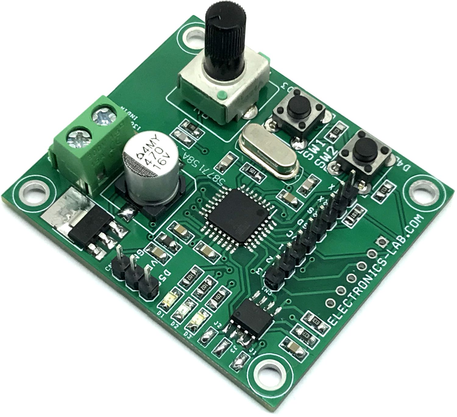
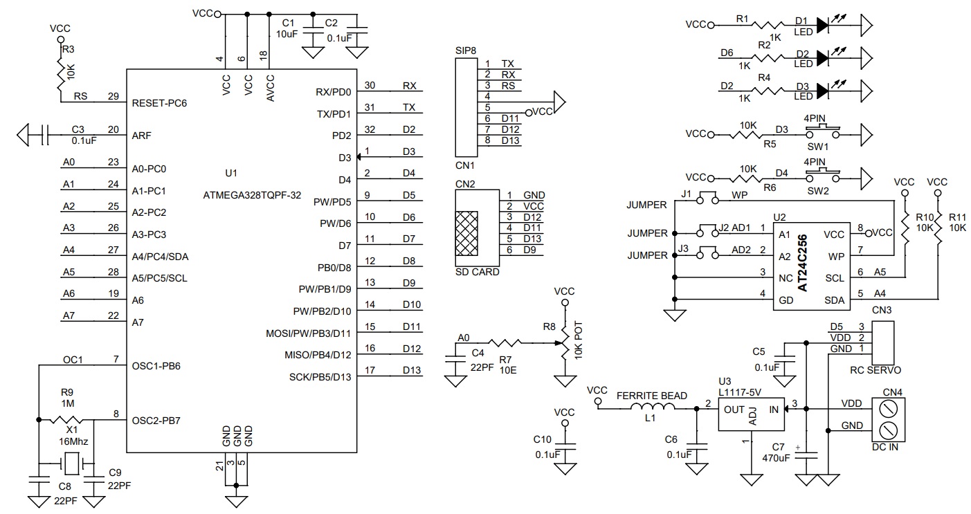
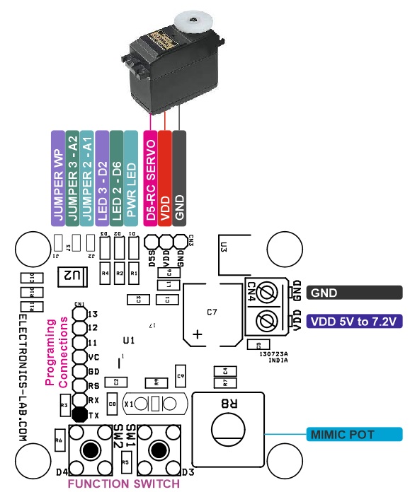
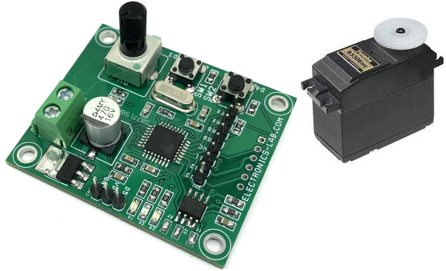
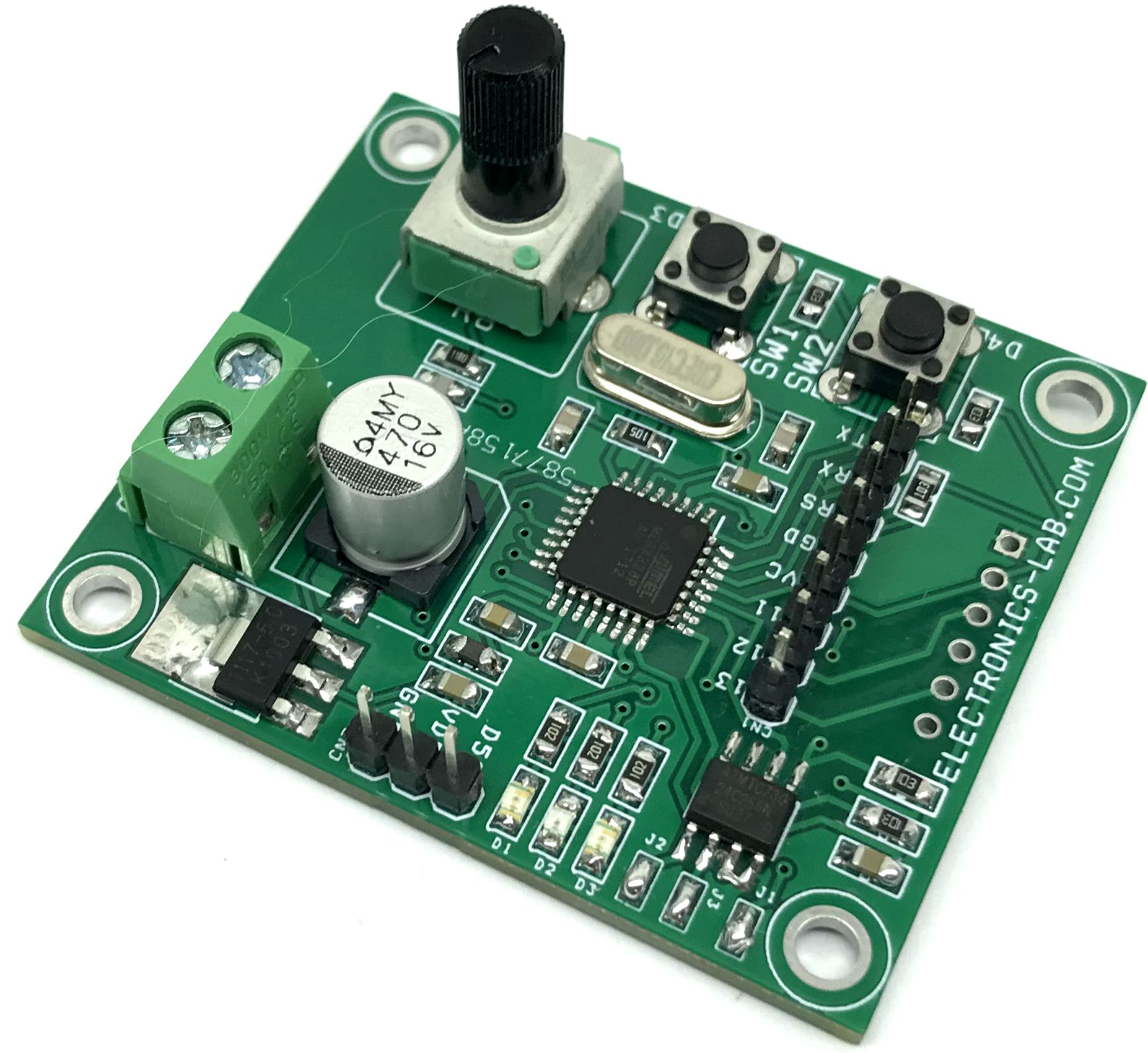
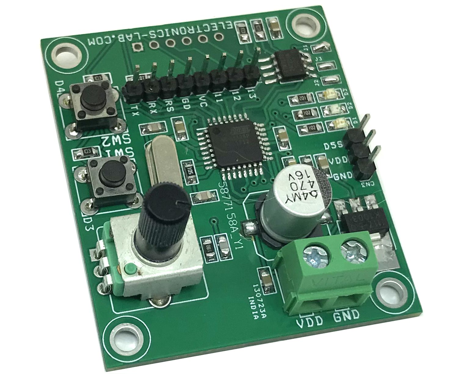
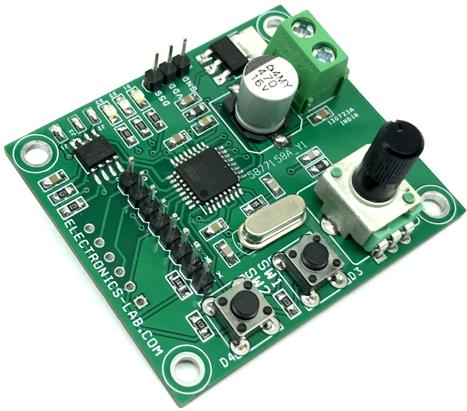
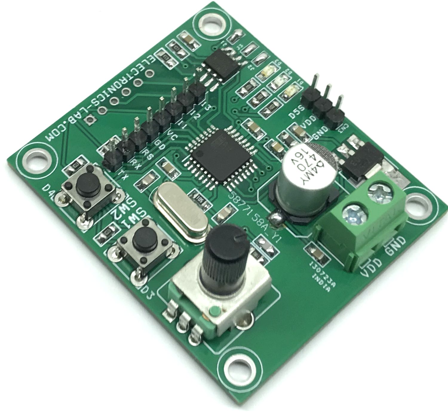
This is an RC servo controller board that allows users to record RC servo motor movement and playback it back with precision. There is an onboard potentiometer to control the RC servo up to 180 degrees. It allows you to record the movement of one servo, a few seconds in duration. Servo movement can be mimicked using the onboard potentiometer. Servo movement data is stored onboard the EEPROM memory chip. The project is Arduino compatible and can be modified to work as a data logger and other applications that require EEPROM and SD Card data logs.
The Arduino code is available as a download and the user will be able to record and playback the RC servo movement for a few seconds with this code. After power is ON, Recording starts when LED D3 lights up, then move the potentiometer to mimic the servo for a few seconds until EEPROM is full and the recording LED is OFF. After a 3-second delay, the Play LED is ON, and playback starts till the end of the movement. This event restarts after 3 seconds.
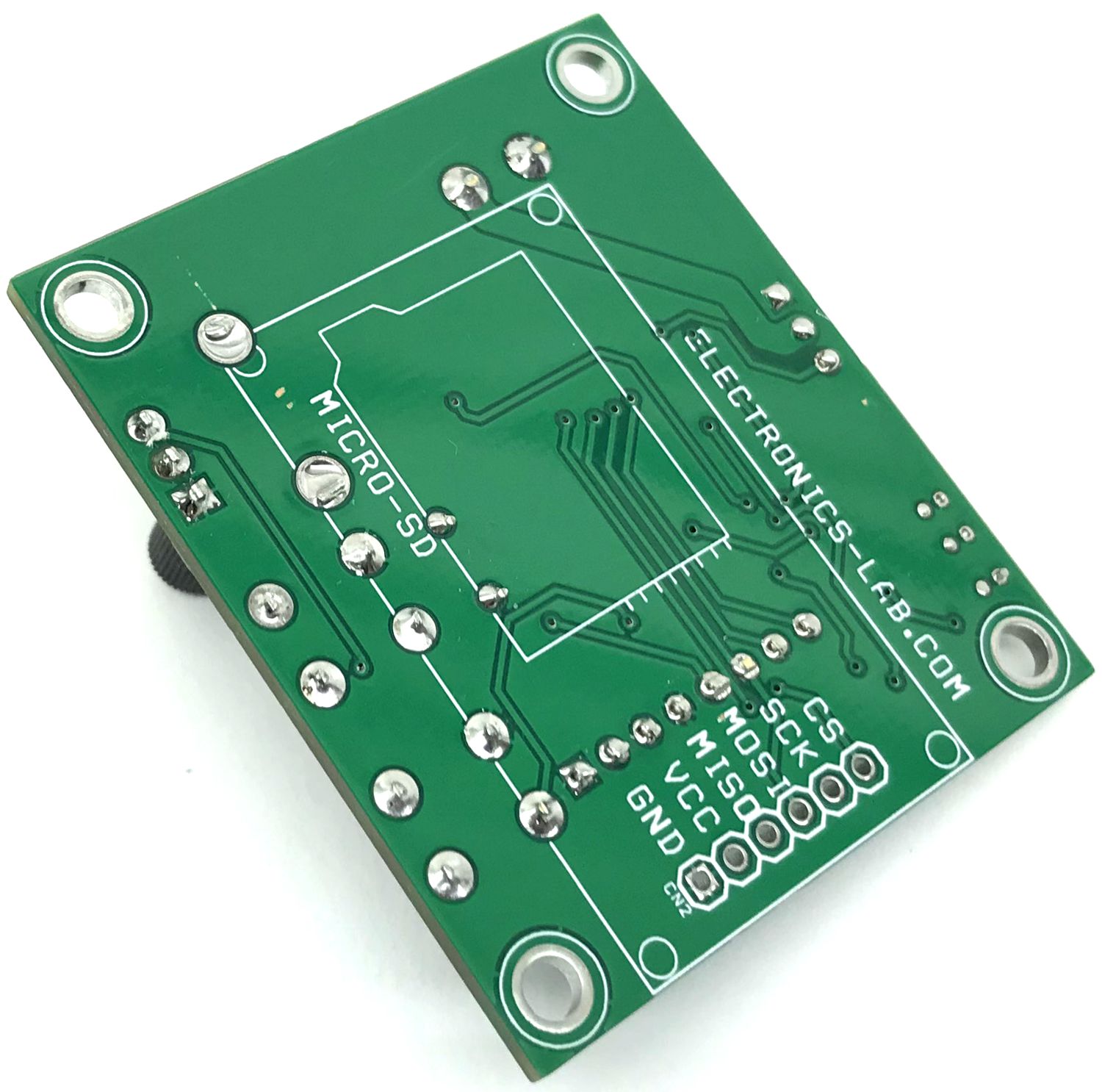
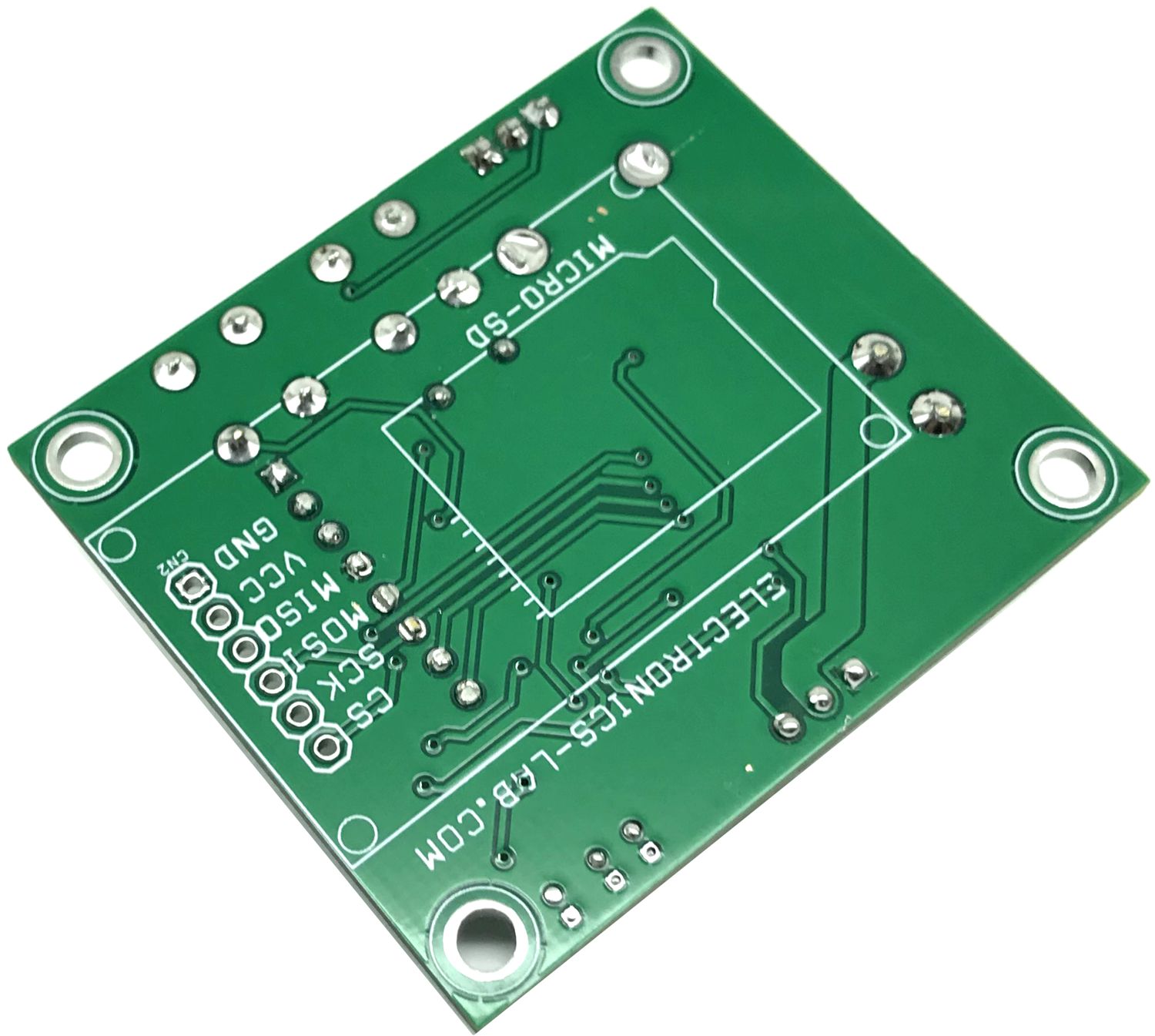
The board has 2 options for data recording. On board EEPROM for low memory size and SD Card module for higher data memory capacity. SD Card module can be installed under the PCB, SD Card module works with SPI protocol and EEPROM follows I2C protocol. Arduino example code works only with EEPROM. The SD card recording requires additional custom code.
Features
Power Supply 5V to 7.2V DC
Atmega328 Micro-Controller
On Board AT24C256 EEPROM
SD Card Module, (Optional option for higher memory). Use CN2 connector to install the SD Card module.
Potentiometer for Analog Input
2 x Tactile Switches with Pull-Up Resistors
Power LED
Record/Playback LEDs
3 Pin Header Connector for RC Servo
SD Card Reader
PCB Dimensions 51.44 x 44.45 mm
4 x 3 mm PCB Mounting Holes
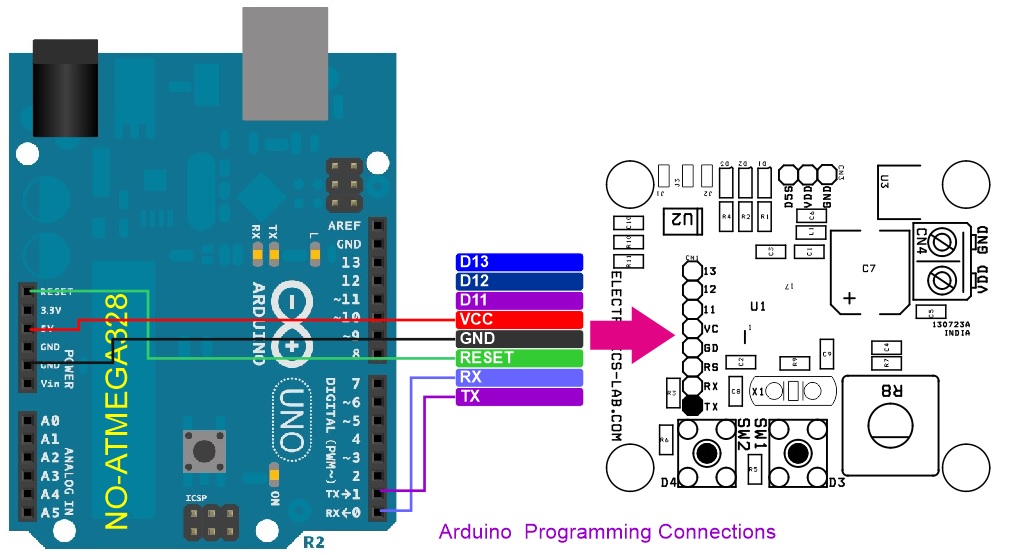
Arduino Programming
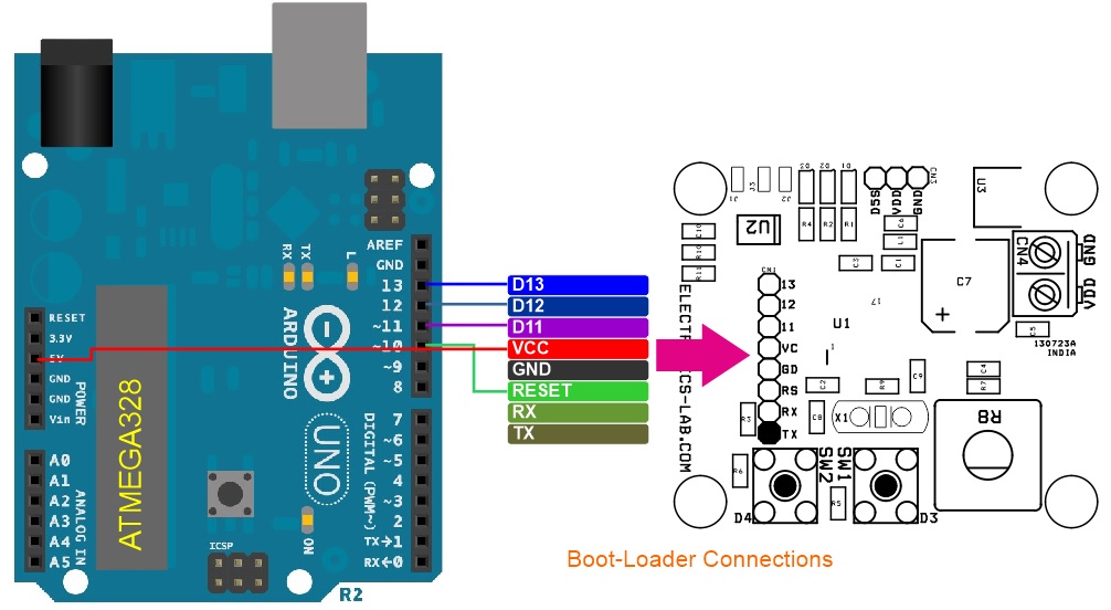
Connector CN1 is provided for bootloader burning and Arduino programming, Follow the link below to learn more about Arduino programming:
A transmission gate is a form of a bilateral switch constructed using Metal Oxide Field Effect Transistors (MOSFETs) that can be externally controlled through logic levels. A switch, analog one to be precise, controls the passage of analog signals through it and is a type of solid-state semiconductor device. The control of these analog switches is processed using digital logic signals. These analog switches are commercially available in different configurations & forms and can be utilized as a transmission gate. These solid-state semiconductor analog switches resemble conventional electromechanical contacts e.g. Normally Close (NC), Normally (NO), Single Pole Single Throw (SPST), and Single Pole Double Throw (SPDT), etc.
The electromechanical relays are quite tedious due to being costly, spacious, and more importantly, their high operating time. Contrary to this, a solid-state switch is made using Metal Oxide Semiconductor (MOS) which makes it superior in terms of operating time, is relatively cheaper and small. A solid-state switch can transmit a signal current through it depending on the logic levels at its control input. One such bilateral switch, CMOS 4016B, is commonly available in the market.
Like other semiconductor devices, Metal Oxide Semiconductor (MOS) devices comprise N-type MOS (NMOS) and P-type MOS (PMOS) devices and can perform logical switching functions. A digital circuit can be deployed to control this logical switching and depending on the type of device, logic levels lead to different operating conditions such as closed or open conditions. A type of solid-state semiconductor switch that allows transmission of signal or data in either direction (both ways) is referred to as a Transmission Gate (TG) and to understand its working principle, it is essential to consider the operation of a Field Effect Transistor (FET) as a basic analog switch.
Solid-state Analog Switch
A simple controlled single-pole switch can be constructed using a Bipolar Junction Transistor (BJT) or a Field Effect Transistor (FET). In terms of construction, a Metal Oxide Semiconductor FET (MOSFET) has an additional layer of metal between the gate terminal and main conducting channel compared to bipolar devices. Additionally, its main conducting channel is purely resistive in characteristics.
The MOSFET as a Switch
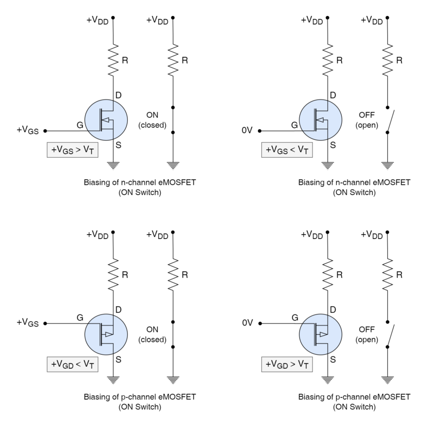
In the following figures, the MOSFET’s basic N-channel and P-channel configurations as a switch have been shown.
Figure 1: N-channel and P-channel MOSFETs as switches
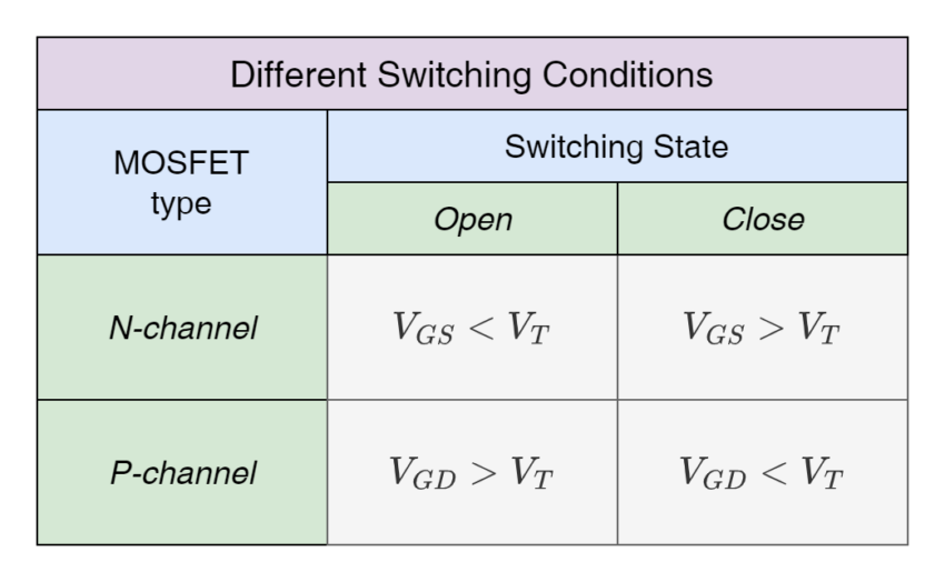
From the above figures, it is observed that certain conditions are required in order to achieve illustrated switching conditions of n-channel (NMOS) and p-channel (PMOS) devices. These conditions refer to a “Threshold Voltage” (VTH) which is the minimum voltage required at the Gate Terminal to initiate conduction in the main conducting channel between source and drain. For an n-channel MOSFET to behave as a closed switch, the VGS (gate-source voltage) must be greater than the VTH (threshold voltage) i.e. VGS > VTH. Whereas, an n-channel MOSFET acts as an open switch when VGS (gate-source voltage) is less than the VTH (threshold voltage) i.e. VGS < VTH. Similarly, a p-channel MOSFET behaves as a closed switch when VGD (gate-drain voltage) is less than the VTH (threshold voltage) i.e. VGD < VTH and it acts as an open switch when VGD (gate-drain voltage) is greater than the VTH (threshold voltage) i.e. VGD > VTH.
The conditions mentioned above required for each switch condition are illustrated in the following table.
Figure 2: Different switching conditions for n-channel & p-channel MOSFETs
The enhancement MOSFET or eMOSFET is commonly used as a switching device that operates in cut-off (OFF state/ open) and saturation regions (ON state/ close). So, VGS (gate-source voltage) or VGD (gate-drain voltage) is controlling voltage to toggle between the OFF or ON state of an enhancement MOSFET.
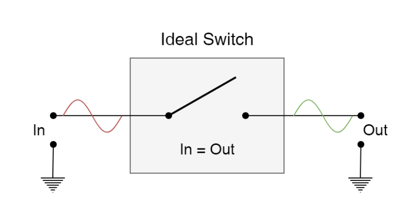
Ideal Switch
The ideal switch is a lossless device somewhat similar to a mechanical switch i.e. it creates a short-circuit in the closed position and an open circuit during open state. Ideally, the signal at input appears at output without any alteration, and an ideal analog switch is shown in the following figure.
Figure 3: An ideal analog switch
However, solid-state switches are not perfect and prone to losses and leakages at different states of operations. These solid-state switches have “ON” state resistances (RON), ranging up to several ohms, causing power losses (I2R) in the form of heat. Whilst their “OFF” state resistances are in kilo-ohms and, as such, they allow passage of a negligible amount of current (Pico amperes) in the main channel. Despite these, enhancement MOSFET is the most widely used switching device that can be effectively controlled by a control voltage applied at its “Gate” terminal.
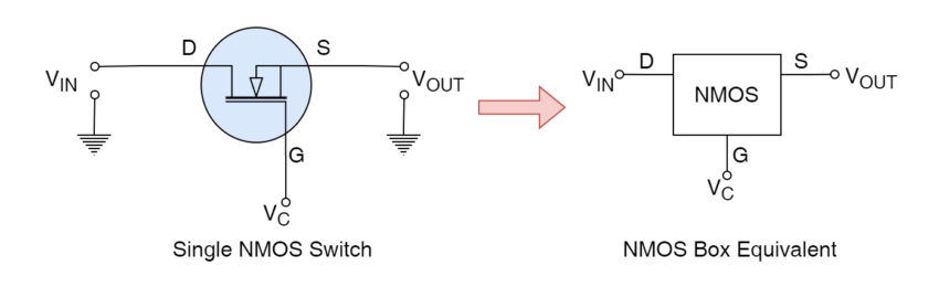
The NMOS Switch as an Analog Switch
An n-channel MOS device allows transmission of analog signals when the input signal is connected to the “Drain” terminal whereas the control signal is applied at the “Gate” terminal. Once the “ON” condition is met, the input signal appears at the output i.e. “Source” terminal. In the following figure, an n-channel MOS (NMOS) along with its block diagram is shown.
Figure 4: An NMOS switch
When input (VIN) and output (VOUT) are connected to the “Drain” and “Source” terminals, respectively, the control input (VC) determines the conduction state of its main channel connecting the “Drain” and “Source” terminals.
When the control voltage (VC) is at LOW state (zero voltage) then NMOS will be in the cut-off region as the “Gate” terminal voltage is not positive with respect to the “Drain” and “Source” terminals. In cut-off operation mode, the conduction path of its main channel remains open and no signal passes from input to output as the “Drain” & “Source” terminals are isolated.
If the control voltage (VC) at “Gate” becomes positive (+) then it turns “ON” the conduction channel of the NMOS device and is said to be operating in the saturation region. This state of the NMOS device resembles the closed state of a switch. In addition, when the “Drain” voltage is more positive compared to the “Gate” terminal, the current flows in the main channel from the “Drain” to “Source” terminals which connects the input (VIN) and output (VOUT) terminals.
However, if input voltage (VIN) becomes zero whilst control voltage (VC) is positive then the main channel becomes open and no current flows through it leading to zero drain-to-source voltage (VDS).
In a nutshell, an NMOS device passes the input signal present at the “Drain” terminal towards its “Source” terminal (output) as long as the control voltage (VC) is HIGH and the NMOS device stops passing the signal to the output, otherwise. The control voltage (VC) is the deciding input for the open and close position of the NMOS device. However, it is important that control voltage (VC) with respect to the source i.e. VGS (gate-to-source voltage) must be kept significantly higher compared to the specific threshold voltage (VTH) of that NMOS device otherwise significant voltage drop and loss will occur at the conduction channel (drain-to-source). As such, an NMOS device is known to pass a weak “HIGH” signal and a strong “LOW” signal through it.
The PMOS Switch as an Analog Switch
The working of p-channel MOS (PMOS) is similar to the NMOS device described above, however, there are some minor differences. In PMOS, the direction of current is from source to drain rather than from drain to source in the case of an NMOS device. Moreover, input and output signals are connected to “Source” and “Drain” terminals, respectively, as shown in the following figure.
Figure 5: A PMOS switch
When a control voltage (VC) of zero magnitude is applied at the “Gate” terminal of the PMOS device and is more negative compared to “Source” & “Drain” inputs then the PMOS device will be operating in the saturation region (closed or ON state). If the “Source” voltage is positive and greater than the applied control voltage (VC) then the current (ID) will flow from the “Source” to the “Drain” terminal which connects the input with the output terminal.
When the input voltage (VIN) at the “Source” terminal is set to zero and, on the other hand, the control voltage (VC) is kept at zero or below zero (negative) voltage then the main conduction channel remains open leading to no current flow state with source-to-drain voltage (VDS) at zero potential gradient. In such a case, input and output terminals are isolated.
When a positive control voltage (+VC) is applied at the “Gate” terminal then the conduction channel of PMOS becomes “OFF” similar to an open-circuit condition and the PMOS transistor is said to be operating in the cut-off region. In this state, no source-to-drain current (ID) flows in the main channel and the input is isolated from the output terminal.
In brief, control voltage (VC) determines the state of the PMOS transistor. When VC is at zero or below zero (negative) potential then the PMOS transistor is operating in the saturation region and conduction between input and output terminals is established (ON state). Whereas, a positive or “HIGH” state input at the “Gate” terminal (VC), sets the operation of the PMOS device in the cut-off region and no conduction occurs between input & output terminals (OFF State).
In PMOS transistors, it is important to keep gate-to-source voltage (VGS) significantly less compared to the Threshold Voltage (VT) of the PMOS transistor enabling it to turn OFF completely otherwise the current will still flow in the conduction channel. Therefore, a PMOS transistor is said to pass a strong “HIGH” signal and a weak “LOW” signal through its channel. On the contrary, as seen above, an NMOS transistor exhibits passing a strong “LOW signal and a weak “HIGH” signal. Thus, looking at the characteristics of NMOS & PMOS devices, it is possible to pass both “LOW” and “HIGH” logics strongly in either direction by combining these MOS devices and this forms the basis of a Transmission Gate.
Transmission Gate
Transmission Gate is a basic bilateral switch formed by connecting NMOS and PMOS devices together in parallel. This parallel symmetry enables bilateral operation i.e. input and output are interchangeable. This CMOS switch has been shown in the following figure by superimposing triangles pointing in opposite directions.
Figure 6: A Transmission Gate & its symbol
The configuration shows the placement of NMOS and PMOS devices in a reverse parallel configuration with an inverter at the input of the “Gate” terminal of the PMOS device to ensure the presence of opposite (complementary) control voltages at the “Gate” terminal of each device. When the control voltage is at “LOW” logic then both NMOS and PMOS devices are in cut-off states and the Transmission Gate opens to isolate input & output. Likewise, when the control voltage is set to a “HIGH” state then both devices are biased into saturation mode, and the Transmission Gate closes to conduct. Therefore, a Transmission Gate is closed when VC = 1 and starts conducting current from either direction whereas it isolates input & output when VC = 0.
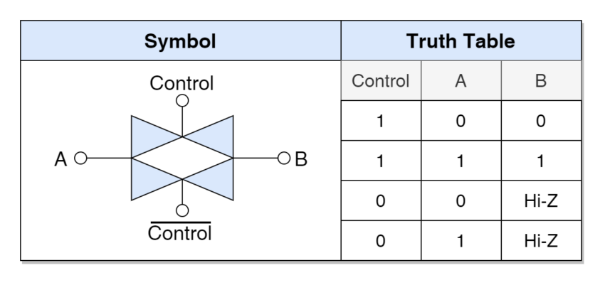
Truth Table and Boolean Expression of a Transmission Gate
Likewise, in other logic gates, a Transmission Gate’s function can be defined using either a Truth Table or a Boolean expression. In the following figure, a Truth Table has been shown of a Transmission Gate along with its symbol.
Figure 7: Truth Table and symbol of a Transmission Gate
It is evident from the Truth Table that the output function of “B” is dependent on both inputs i.e. “A” & “Control”. However, output at the “B” terminal is always “Hi-Z” irrespective of the “A” terminal input as long as “Control” is set to “0”. This resembles an AND operation of inputs “A” & “Control” which eventually yields a Boolean expression of a Transmission Gate as defined below:
The Boolean expression requires a 2-input standard AND gate with inputs “A” and “Control” as operands to implement it as shown in the following figure.
Figure 8: An equivalent logic of Transmission Gate
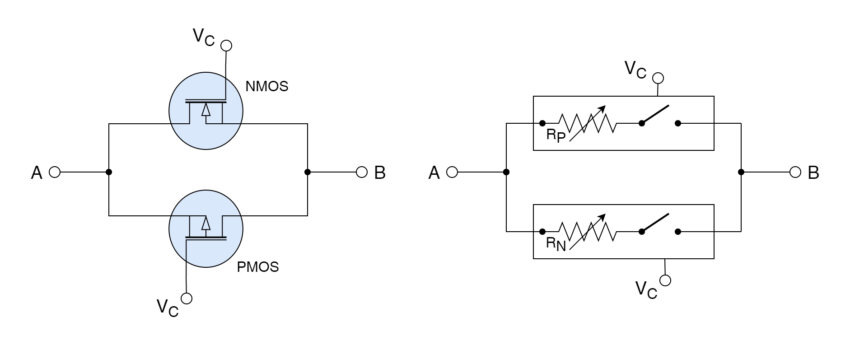
As shown earlier, each of these MOS devices can independently act as a switching device and presents an On-resistance (RON) during conduction. However, their parallel configuration in the form of a Transmission Gate effectively reduces the On-resistance (RON) during the conduction even though either of the MOS devices conducts depending on the direction of current or input & output selection. Whilst, a non-conducting MOS device, presents a several thousand ohmic resistance but overall parallel On-resistance (RON) effect of conducting and non-conducting MOS devices remains quite low compared to the On-resistance (RON) of an individual device. This is demonstrated using the following figure.
Figure 9: RON of a transmission gate
Conclusion
An ideal analog switch is a lossless switch somewhat identical to a mechanical switch. It creates a short circuit, having nearly zero resistance, when closed and open-circuited by physically isolating input and output terminals.
A solid-state switch is small, cost-effective, and very responsive to switching operations. Their states are controlled through an additional input using a “Control” signal. However, it has some losses associated with each of its switching states. In a closed state, it has a specific On-resistance (RON) causing I2R losses in form heat and carries a leakage current in the open state as well.
A Metal Oxide Semiconductor Field Effect Transistor (MOSFET) can also act as a switching device besides a Bipolar Junction Transistor (BJT) and offers several advantages over BJT switches.
An n-channel MOS device has input and output signals connected to “Drain” and “Source” terminals, respectively. It conducts when the Control Voltage is set to “HIGH” and conduction stops when it is set to “LOW” state. An NMOS device is a good transmitter of “LOW” signals and a poor transmitter of “HIGH” signals.
A p-channel MOS device has input and output signals connected to “Source” and “Drain” terminals, respectively. It does not conduct when the Control Voltage is set to “HIGH” and starts conducting when it is set to “LOW” state. A PMOS device is a good transmitter of “HIGH” signals and a poor transmitter of “LOW” signals.
A Transmission Gate is a bilateral switch formed by combining NMOS and PMOS devices in a reverse parallel configuration and, as such, holds the characteristics of both NMOS and PMOS devices i.e. it is a good transmitter of both “LOW” and “HIGH” states.
A Transmission Gate acts as a closed switch when the Control Voltage (VC) is set to “HIGH” and as an open-circuit when the VC is set to a “LOW” state. Moreover, it presents a lower On-resistance (RON) compared to individual MOS devices acting as a switch.
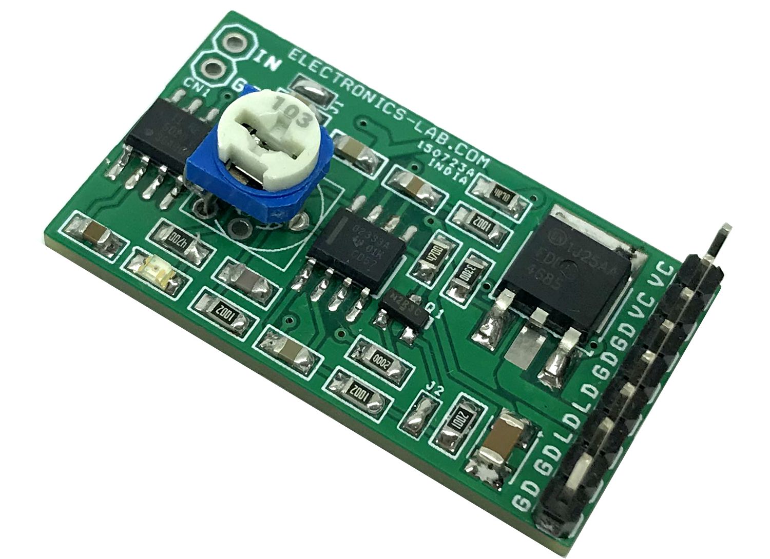
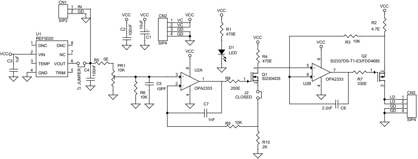
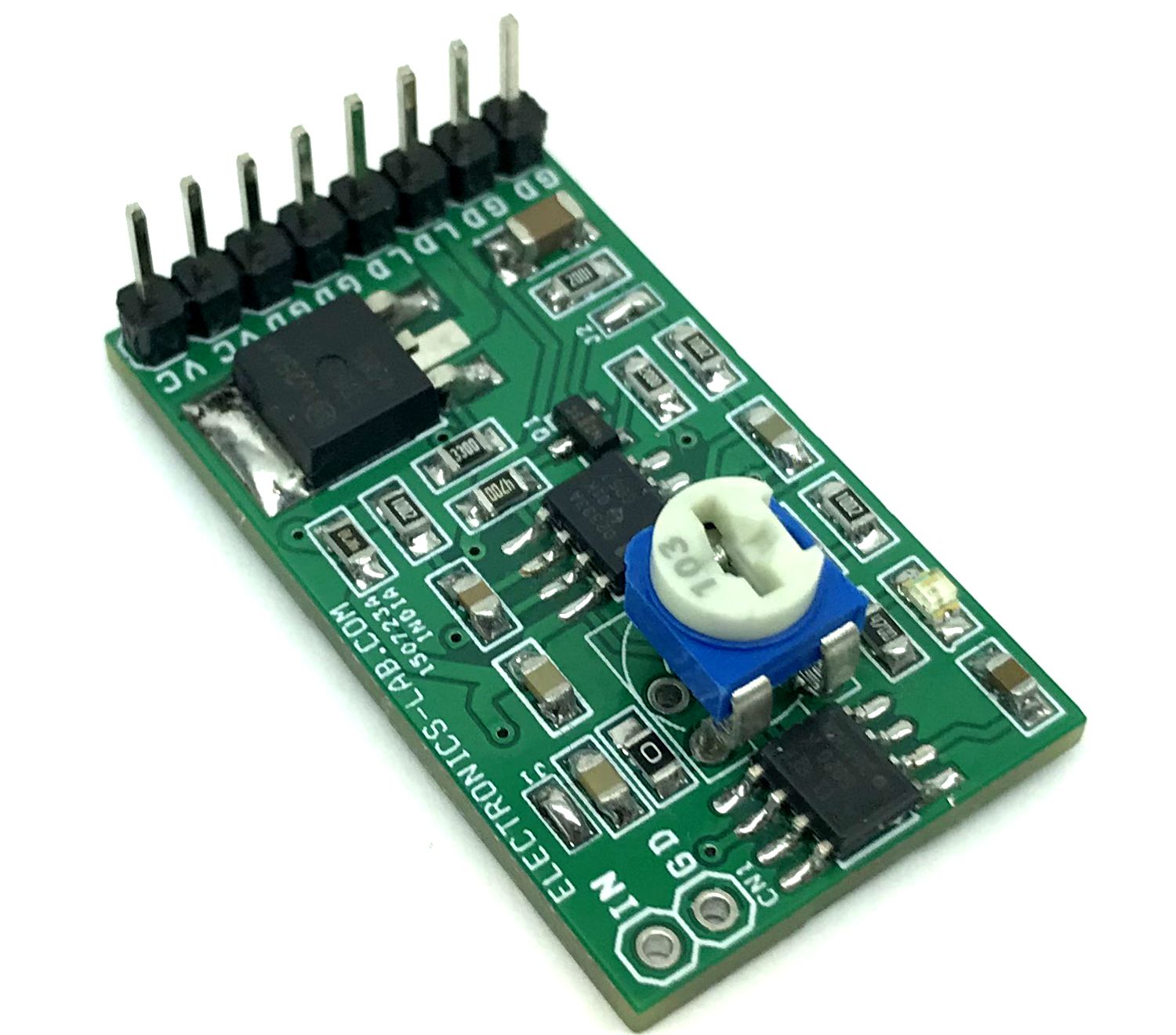
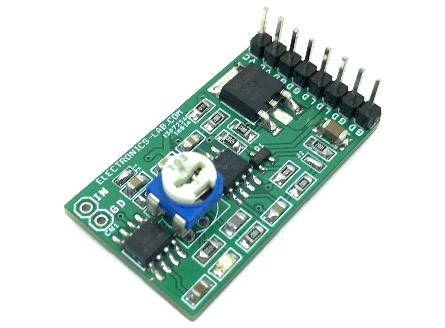
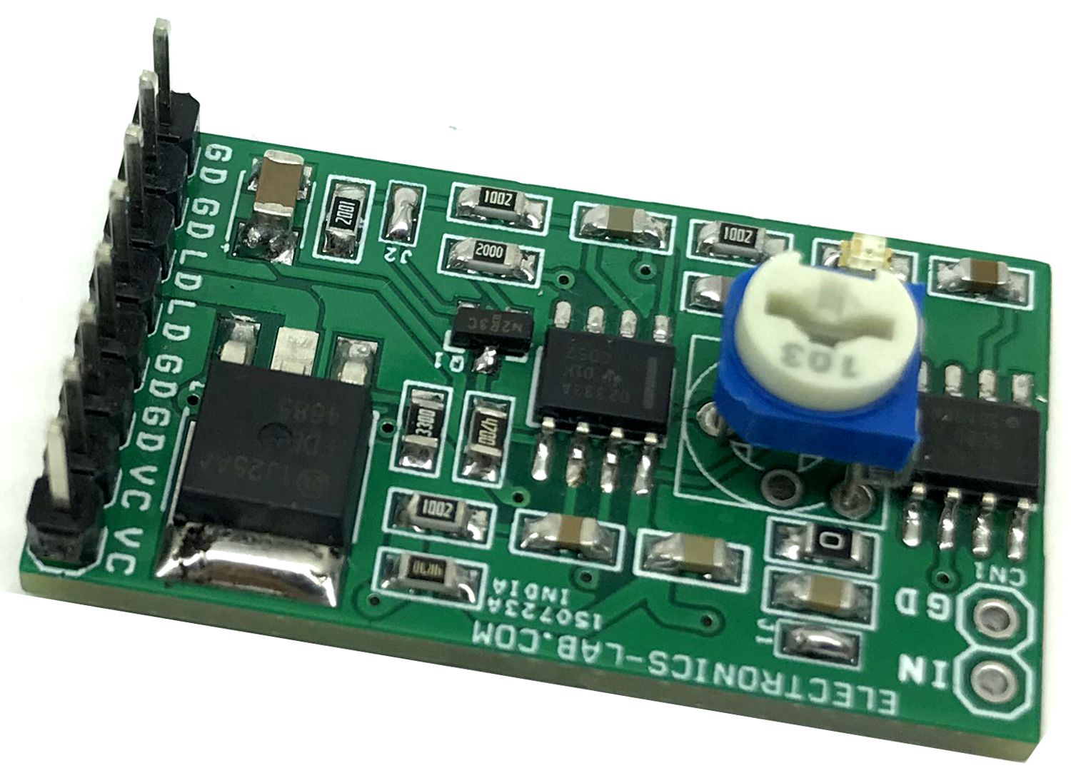
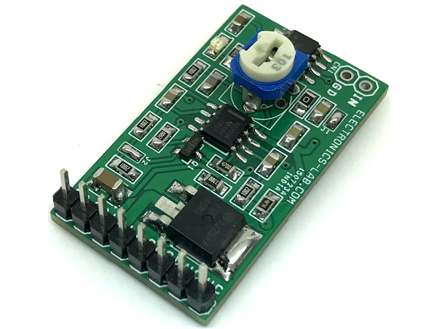
The circuit shown here is a high-side voltage-to-current (V-I) converter. It translates an input voltage of 0 V to 2 V to an output current of 0 mA to 100 mA. The low offset voltage and offset drift of the OPA2333 facilitate excellent DC accuracy for the circuit.
The project provides a high-side current source that supplies an adjustable current to a ground reference load. The first op-amp stage sets a reference current based on the input control voltage. The second op-amp stage acts as a current mirror that gains the reference current and regulates the current sourced from the output PMOSFET Q2 to the load. R2, R4, and R10 set the output current based on the input control voltage. Components C7, R9, R8, R7, C6, R3 provide compensation to ensure stability of the circuit.
The V-I transfer function of the circuit is based on the relationship between the input voltage, VIN, and the three current sensing resistors, R2, R4, and R10. The relationship between VIN and R10 determines the current that flows through the first stage of the design. The current gain from the first stage to the second stage is based on the relationship between R2 and R4. The project is built using OPA2333. Low offset voltage, low-temperature drift, and rail-to-rail output are the key features of this op-amp. The OPA2333 CMOS operational amplifier is a high precision, 5-uV offset, 0.05-μV/°C drift amplifier optimized for low-voltage, single-supply operation with an output swing to within 50 mV of the positive rail. The OPA2333 family uses chopping techniques to provide low initial offset voltage and near-zero drift over time and temperature. Low offset voltage and low drift reduce the offset error in the system, making these devices appropriate for precise DC control. The rail-to-rail output stage of the OPA2333 ensures that the output swing of the operational amplifier is able to fully control the gate of the MOSFET devices within the supply rails.
Note: Use high-precision, low-drift resistors for R2, R4, and R10 to minimize errors caused by resistor mismatch and temperature drift.
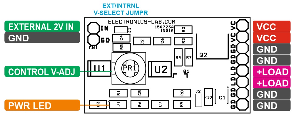
Control Voltage Input: The project works with external or internal control voltage.
U1 REF5020 generates accurate 2V. Solder jumper J1 for internal control voltage, Trimmer potentiometer PR1 is provided to adjust the control voltage 0 to 2V.
For external control voltage input, open the jumper J1, CN1 provided to feed the external control voltage 2V, PR1 can be used to adjust the 0 to 2V.
Features
Input Supply 5V DC
Input Control Voltage 0 to 2V
Output 0 to 100mA
Jumper For External/Internal Control Voltage Selection
Reference Voltage Generator Chip for 2V Control Voltage Source
Header Connector for Input and Output and Power Supply
On Board Power LED
On Board Trimmer Potentiometer for Control Voltage Adjustment
The new Broadcon EMT507 single board computer for automotive applications is powered by a cost-optimized MINI507 system-on-module equipped with Allwinner T507-H industrial processor, 2GB/4GB RAM, and 8GB/16GB/32GB/64GB eMMC flash.
One major highlight of the EMT507 SBC is that it is built around the Allwinner T507-H 4-core Arm Cortex A-53 chip, running at up to 1.5 GHz and with an ARM Mali-G31 MP2 GPU. The chip is a high-performance one designed for the new automotive markets and works perfectly for automotive industrial applications. It was even said that it has undergone Automotive AEC-Q100 testing already. The processor supports full-format video playback, multi-video output interfaces, and a rich set of other interfaces which greatly facilitates product expansion. It comes with great combination of feature set such as 4K@60fps H.265 video decoder, 4K@25FPS H.264 video encoder, 4x USB, 2x Ethernet MAC, 6x UART, 6x TWI, 4x GPADC, HDMI 2.0a up to 4K@60fps and 1080@60fps RGB interface
Though the EMT507 SBC comes with a 2GB RAM memory size and 8GB flash for storage, it leaves room for upgrade to enable its users to have a smooth multitasking, responsive, and flexible operation experience. The board also provides flexible options for network connectivity, a wide range of display connectivity, and a means to deliver high-definition multimedia content.
Features and Specifications include:
SoC:
Allwinner T507-H 4-core Arm Cortex A-53 chip, running at up to 1.5 GHz
ARM Mali-G31 MP2 GPU with support for OpenGL ES 1.0/2.0/3.2, Vulkan 1.1, OpenCL 2.0
4K@60fps H.265 video decoder and 4K@25FPS H.264 video encoder
HDMI 2.0a up to 4K@60fps, 1080@60fps RGB interface
4GB DDR4 memory size
64GB eMMC flash
1x microSD card slot
2x RJ45 ports
3.5mm audio jack
1x Serial port, 3x UART, and 1x RS232
2x USB 2.0 host and 1x USB 2.0 OTG
Wireless connectivity – 1x each of GbEthernet and 10/100 Mbps LAN ports, 2.4G WiFi, Bluetooth 5.2, mPCIe with Nano SIM card port (for 4G cellular connectivity)
Multiple Camera Interfaces – 1x DPV camera, 4x AHD Cameras
1x 2-channel LVDS, 1x HDMI 2.0a
1x Real Time Clock, IR receiver
Power: 12V/3A DC
Baseboard Size: 150 mm x 110 mm
CPU Size: 65 mm x 51 mm
OS: Android 10
While the board can be used conveniently for a variety of applications, the company says it is perfect for application scenarios such as digital cluster, HD AVM (Around View Monitor), Intelligent Cockpit, and In-Vehicle Infotainment.