PGCPSU the tiny, powerful & affordable LiPo PSU module

Pretty Good Cheap Power Supply Unit – PGCPSU. Get the best tiny power supply for your battery powered projects!

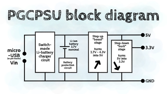
PGCPSU is a three in one power supply board: it integrates a lithium battery charge management circuit with 5V and 3.3V DC-DC converter-based output rails to power most projects in a very compact form factor. We took special care in selecting inexpensive yet well-fitting parts to make up for a great little power(ful) supply!

Features

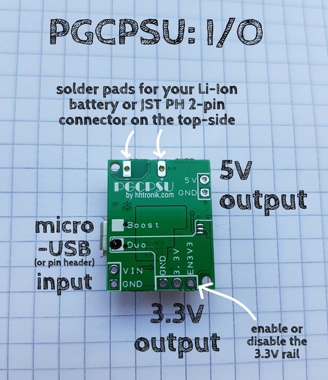
  • Power Input – micro USB input or pin header for charging (4.7V to 6V max.)
  • Power Output
    • 5V rail providing at least 350mA, and up to 650mA
    • 3.3V rail providing at least 400mA, and up to 800mA
  • Safety
    • Integrated battery protection including reverse polarity protection
    • Over-discharge, short circuit/over-current protection
  • Power Efficiency
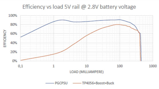
    • High efficiency even at low load, important for long battery life
    • Low quiescent current (49uA for the 5V rail + 57uA for the 3.3V rail)
    • Enable/disable pin for the 3.3V rail with selectable default state solder jumper
  • Charging –  Quick charging at up to 1.9A (fully charges a 2,600mAh cell in about 2 hours)
  • Dimensions – 25x20mm

The module can also be used as an uninterruptible power supply.

PGCPSU is live on Kickstarter with a €1,250 funding target. Rewards start at 7 Euros for a PGCPSU DUO (5V/3.3V) module and a PGCPSU Boost (5V only) module, but once all early bird rewards are gone price for PGCPSU Duo is offered for 11 Euros, or you may consider a starter kit with a DUO module plus a 2,600 mAh 18650 LiPo battery. Shipping adds a further 7 Euros, and backers can expect their rewards between May and August 2019 depending on the selected perk.

LG and Infineon to introduce LG G8ThinQ with front-facing Time-of-Flight camera

With Infineon’s REAL3™ Image Sensor Chip, LG Offers Enhanced Security and Depth Measuring Selfie Camera

LG Electronics and Infineon Technologies AG have teamed up to introduce leading edge Time-of-Flight (ToF) technology to smartphone selfie photo lovers world over.

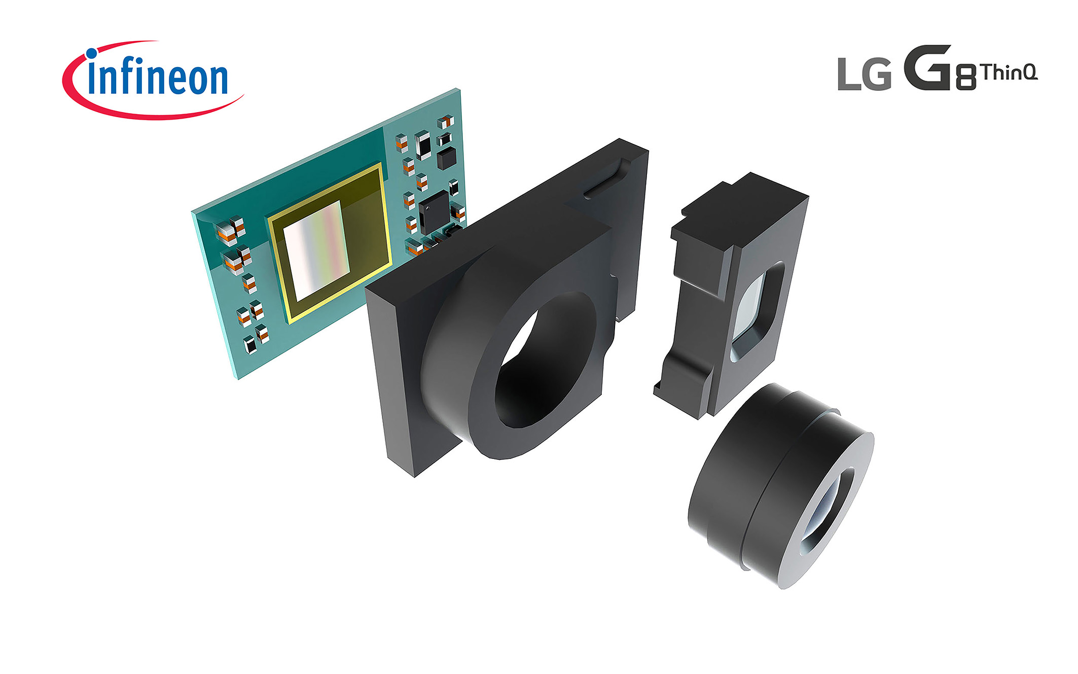
Infineon’s REAL3™ image sensor chip will play a key role in the front-facing camera of the upcoming LG G8 ThinQ, to be unveiled in Barcelona during Mobile World Congress 2019. Building upon the combined expertise of Infineon and pmdtechnologies in algorithms for processed 3D point clouds (a set of data points in space produced by 3D scanning), the innovative sensor will deliver a new level of front camera capability in a smartphone.

While other 3D technologies utilize complex algorithms to calculate an object’s distance from the camera lens, the ToF image sensor chip delivers more accurate measurements by capturing infrared light as it is reflected off the subject. As a result, ToF is faster and more effective in ambient light, reducing the workload on the application processor thereby also reducing power consumption.

And due to its fast response speed, ToF technology is widely used in various biometric authentication methods, such as face-recognition. What’s more, because ToF sees objects in 3D and is not affected by light from external sources, it delivers an excellent recognition rate, both indoors and out, ideal for implementation in augmented reality (AR) and virtual reality (VR) applications.

The world’s leading manufacturer of power semiconductors, Infineon is also recognized for its technological excellence in sensor solutions. The German chip maker enables highly reliable automotive, power management and digital security applications. The company developed the ToF technology featured in the LG G8 ThinQ for use in both premium, high-end smartphones as well as mid-end devices.

Infineon is poised to revolutionize the market, said Andreas Urschitz, division president of Infineon’s Power Management & Multimarket division.

We have demonstrated service beyond the mere product level – specifically catering to phone OEMs, associated reference design houses and camera module manufacturers. Within five years, we expect 3D cameras to be found in most smartphones and Infineon will contribute a significant share.

Keeping in mind LG’s goal to provide real value to its mobile customers, our newest flagship was designed with ToF technology from inception to give users a unique and secure verification system without sacrificing camera capabilities,

said Chang Ma, senior vice president and head of Product Strategy at LG Mobile Communications Company.

The LG G8 ThinQ featuring ToF will be the optimal choice for users in search of a premium smartphone that offers unmatched camera capabilities.

Further information about REAL3™ is available at www.infineon.com/real3

Linear LED controller ICs target dimmable lighting applications

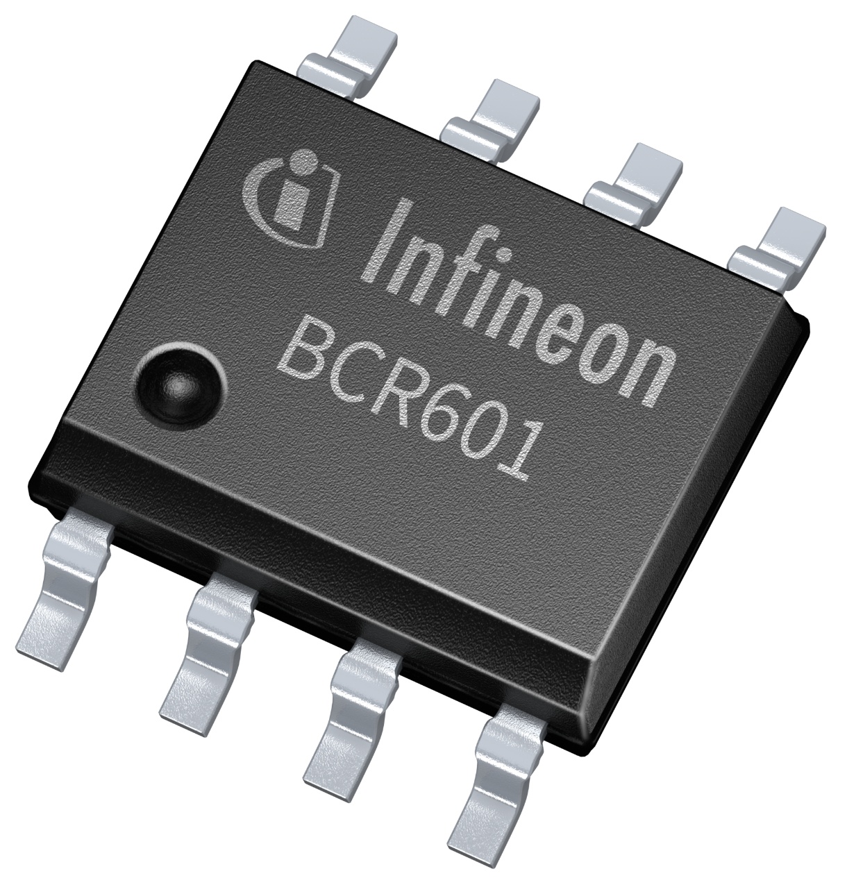
Two linear LED controller ICs have been added to the BCR portfolio, by Infineon Technologies. The BCR601 has voltage feedback to the primary side (also known as active headroom control or AHC), for cost effective and power efficiency LED driver applications.

The BCR602 targets dimmable LED applications such as light engines, modules and strips. It has a wide voltage range of up to 60V makes it suitable for 48V designs and DC/DC grids, confirms Infineon.

The supply voltage of both LED controller ICs ranges from 8.0 to 60V up to the SELV limit. Both the BCR601 and BCR602, operate with an external driver transistor, either an NPN bipolar transistors or an N-channel MOSFET to support a wide LED current and power range.

The ICs allow the LED current to be adjusted by resistors as well as dimmed analogue. The BCR602 also accepts digital PWM up to 3.5 kHz and combined dimming.

Both the BCR601 and BCR602 represent an inherent AC ripple suppression, driving a constantly stable LED current to prevent light flicker.

The AHC of the BCR601 allows controlling the output voltage of the primary side converter such as the XDPL8218 flyback controller from Infineon. This architecture helps a linear LED controller to achieve maximum system efficiency by actively adjusting the AC/DC feedback loop to set minimum voltage headroom.

Adjusting the minimum necessary voltage across the pass transistor optimises system efficiency which can normally only be achieved by secondary switched mode device, points out Infineon, to reduce component temperatures and stress. This construction also reduces EMI compared to switched mode supplies in combination with a low bill of materials, adds Infineon. Additionally, the BCR601 features an adjustable over-voltage protection to prevent any damage to the LEDs.

Both ICs also offer embedded hot-plug protection. This allows connecting or disconnecting the LED load without power down protecting the LEDs from electrical over-stress events. The over-temperature protection reduces the LED current by 30 per cent of the nominal current as soon as the junction temperature exceeds the defined threshold. The LED controller ICs resume regular operation as soon as the temperature drops below the hysteresis.

http://www.infineon.com

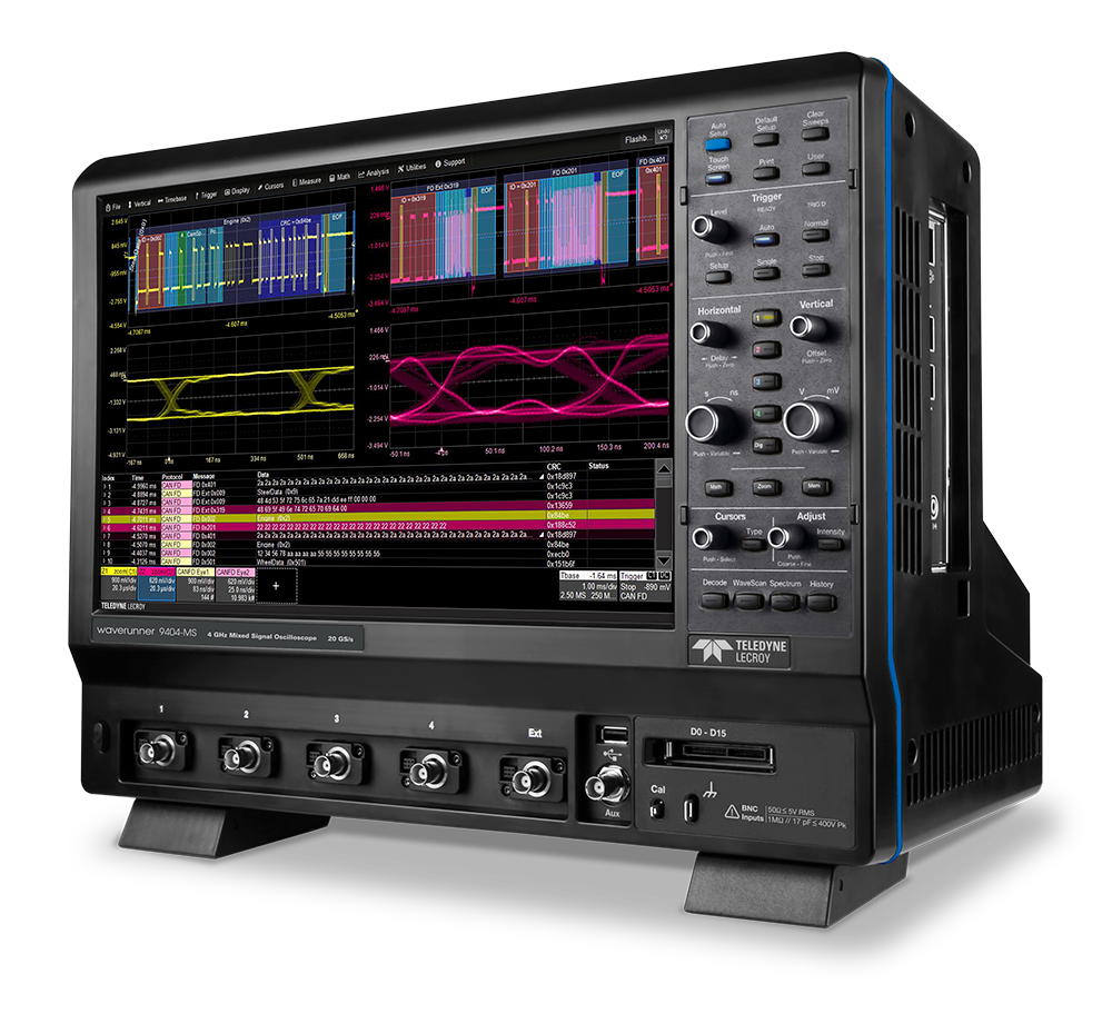
Teledyne LeCroy Introduces WaveRunner 9000 Oscilloscopes with 15.4” Display

Teledyne LeCroy today introduced its WaveRunner 9000 Series mixed-signal oscilloscopes with a large, 15.4” display, bandwidths from 500 MHz to 4 GHz, and sample rates up to 40 GS/s. The WaveRunner 9000 Series offers the industry’s deepest toolbox and the most complete collection of serial data debug and validation solutions, making it ideal for embedded system, automotive, and EMC/EMI test applications.

The ubiquity of embedded computing systems with high-speed microprocessors drives industry demand for mid-range, mixed-signal oscilloscopes with high bandwidth and powerful debug and validation toolsets. However, equipment budgets have not kept pace with the increase in microprocessor speed and complexity. This has forced engineers and managers to sacrifice certain capabilities in their test equipment. Teledyne LeCroy’s WaveRunner 9000 oscilloscopes offers all of the critical features—a large display, powerful toolbox, wide range of bandwidths, and enhanced resolution up to 11 bits—at an affordable price.

The WaveRunner 9000 Series offers the industry’s deepest toolbox with a large 15.4” display at a price point that does not require engineers to sacrifice features or performance,” said Tyler Cox, VP and general manager for oscilloscopes/digitizers. “The vast serial data coverage of these new oscilloscopes makes them perfect for embedded/automotive testing, and the 40 GS/s sampling rate is ideal for EMI/EMC testing.

About the WaveRunner 9000

The WaveRunner 9000 offers a huge array of test, debug, and validation tools, making it well suited for comprehensive testing of embedded computing systems. The widest selection of serial data triggering and decode (TD) packages provides powerful, flexible serial triggering with an intuitive color-coded decode overlay. Additionally, unique measure/graph and eye-diagram test (TDME) packages complement the TD packages by enabling extraction of decoded data and subsequent waveform data plots, performing bus timing measurements, and creating eye diagrams for testing against standard or custom masks. This set of tools provides exhaustive causal analysis for not only embedded systems but also automotive applications, covering all aspects of Automotive Ethernet validation and debug, including 1000Base-T1 and 100Base-T1 compliance test.

WaveRunner 9000 oscilloscopes have standard capability to provide improved resolution with bandwidth tradeoffs by means of filtering, and each channel can be filtered independently. The filtered result shows the improvement in the number of effective bits at a given bandwidth.

For EMC/EMI compatibility applications, WaveRunner 9000 accurately characterizes EMC test signals with a 40 GS/s sampling rate and 1% gain accuracy. The WaveRunner 9000’s spectral analysis mode pins down high harmonic peaks across a wide EMC band using an interactive peaks and markers table. In addition, a dedicated EMC pulse parameter measurement package enables the user to tailor measurements to specific EMC/ESD standards.

Price and Availability

The WaveRunner 9000 oscilloscopes start at $16,435 and are available now. An extensive range of probes is optionally available to serve virtually any probing requirement.

Slimline NVMe SSD outperforms SATA models

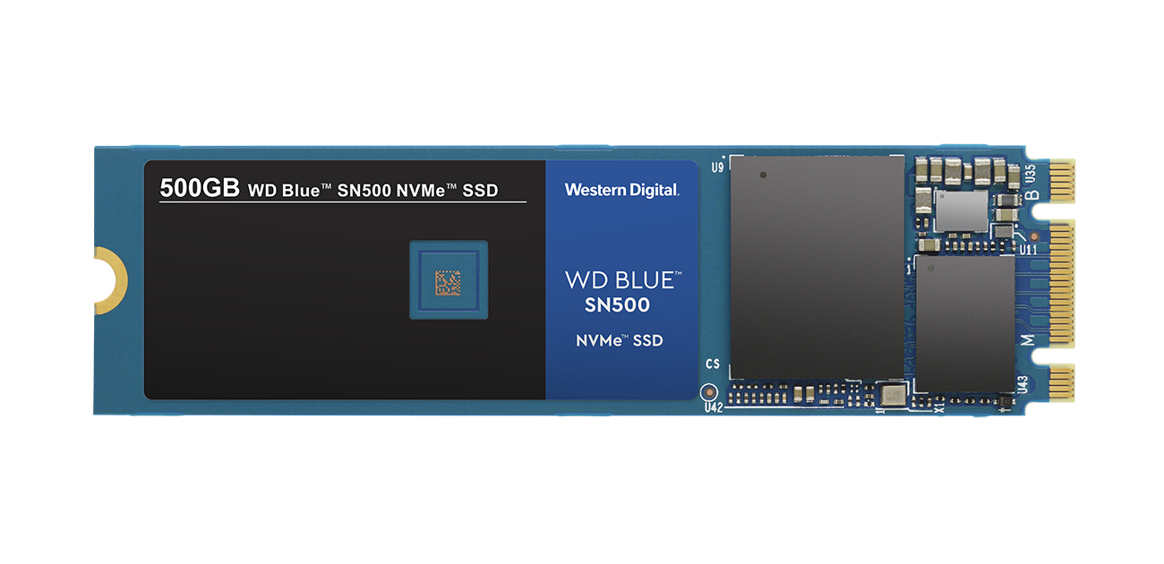
Western Digital Corp. , a global data infrastructure leader, is accelerating the NVMe transition of value-PC storage by adding an NVMe™ model to its award-winning WD Blue® solid state drive (SSD) portfolio, the WD Blue SN500 NVMe SSD. The new SSD delivers three-times the performance of its SATA counterpart1 while maintaining the reliability the WD Blue product line is known for. For content creators and PC enthusiasts, the WD Blue SN500 NVMe SSD is optimized for multitasking and resource-heavy applications, providing near-instant access to files and programs.

Leveraging the scalable in-house SSD architecture of the highly acclaimed WD Black® SN750 NVMe SSD, the new WD Blue SN500 NVMe SSD is also built on Western Digital’s own 3D NAND technology, firmware and controller, and delivers sequential read and write speeds up to 1,700MB/s and 1,450MB/s respectively (for 500GB model) with efficient power consumption as low as 2.7W.* Since demands on storage are continuing to grow and client workloads are evolving, the WD Blue SN500 NVMe SSD features high sustained write performance over SATA as well as other emerging technologies on the market today to give that performance edge.

The PC industry continues its transition from SATA to the NVMe protocol, along with the expectation from consumers that computers continue to become faster and more responsive, said Don Jeanette, TrendFocus.

Within the mainstream segment, content creators are consistently doing more, such as editing 4K or 8K video files, creating and streaming content, and managing massive amounts of data internally. The new WD Blue SN500 NVMe SSD will enable larger file loads that require faster storage.

Content transitioning from 4K and 8K means it’s a perfect time for video and photo editors, content creators, heavy data users, and PC enthusiasts to transition from SATA to NVMe, said Eyal Bek, vice president marketing, data center and client computing, Western Digital.

The WD Blue SN500 NVMe SSD will enable customers to build high-performance laptops and PCs with fast speeds and enough capacity in a reliable, rugged and slim form factor.

Perfect in slim form factor notebooks or desktop PCs, the WD Blue SN500 NVMe SSD will be available in 250GB and 500GB capacities in a single-sided M.2 2280 PCIe Gen3 x2 form factor. Manufacturer’s Suggested Retail Price (MSRP) in the U.S. is $54.99 USD for 250GB (model number: WDS250G1B0C) and $77.99 USD for 500GB (model number: WDS500G1B0C). For more information, visit the website: Western Digital.

Intel Wi-Fi 6 AX200 Launches With Linux Support

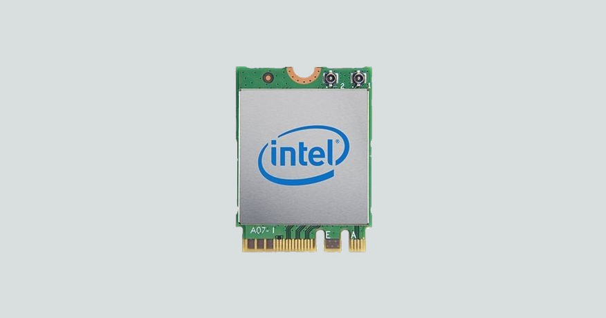
WiFi 6 (aka 802.11ax) can deliver up to 10 Gbps in theory, and provides better handling of high density scenario in train stations, conferences, etc… We’ve seen it implemented in some routers and smartphones, but most laptops don’t support the new WiFi standard, so in order to solve this little issue, Intel has now launched AX200 M.2 WiFi 6 card in the M.2 2230 and M.2 1216 form-factors.

The AX200 uses an M.2 2230 form factor, supports a max speed of 2.4Gbps, and supports Bluetooth 5. The AX200 parts will be available at $10 to $17 USD.

Drivers are/will be available for Windows 10 64-bit, Google Chrome OS, and Linux via the “IWLWIFI” driver.

for a little more information visit: ark.intel.com

CM3 PLAYER Carrier Board for Raspberry Pi CM3+ Targets LVDS Displays

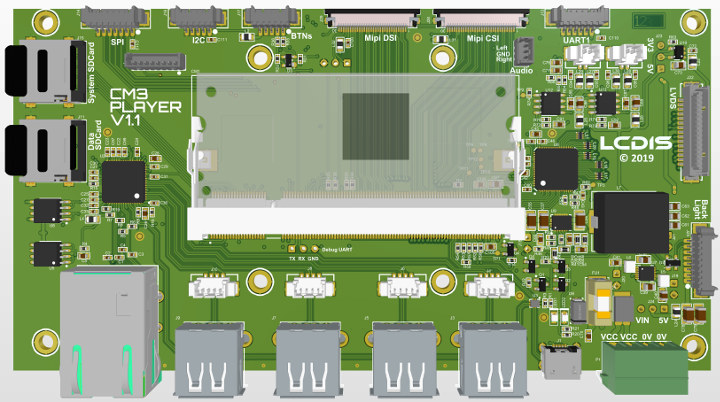
LCDIS, a French company specialized in embedded & display solutions, has been working on a carrier board for Raspberry Pi Compute Module 3+ designed to drive displays used in industrial applications such as digital signage and HMI. For that purpose, CM3 PLAYER exposes LVDS, backlight, and MIPI DSI connectors, as well as Ethernet, four USB ports, and over I/Os.

CM3 PLAYER specifications:

  • Compute Module – Supports CM3 with built-in eMMC or external SD card
  • Storage – 2x microSD card slots, one for data, one for OS
  • Display I/F
    • Single or dual channel LVDS up to 1920×1080
    • MIPI DSI connector
  • Camera I/F – MIPI CSI connector
  • Audio – 2x 2.5W Class D amplifier, audio line output, speaker output
  • Networking – 10/100M Ethernet
  • USB – 4 x USB (type A with MOLEX 53261 in parallel)
  • Expansion Headers – I2C, SPI, UART, 6x GPIO, buttons (BTNs) headers
  • Power Supply – 9-36VDC power input via terminal blocks; Note: some backlight drivers will require 12V, while other require 24V.
  • Dimensions – 155 x 80 mm; 4 mounting holes for optional heatsink or fan
  • Temperature Range – -20° to +70°C

The board has not been produced yet, and the first samples are scheduled for May 2019. The company plans to sell the board with a selection of displays pre-configured for the board and accompanying custom cables.

While the company plans to sell the board as it is, most customers will want to customize it, and LCDIS explained us they plan do so at a very low MOQ, and afforable NRE. Some of the customization may include a second LVDS output, PoE function, battery operation, Ethernet switch, 4G modem support, and more.

CM3 PLAYER is not yet listed on the company website, and they just made an announcement on LinkedIn (French language) so far.

via www.cnx-software.com

Top 10 Upcoming Linux Boards to watch in 2019

We have seen a series of Linux-based SBCs the last few months, like the next-gen BeagleBone AI, maker boards from Google and Nvidia, to mention just a few. The SBC market is booming right now, infact a recent Global Market Insights report projects that the SBC market will grow from $600 million in 2018 to $1 billion by 2025. The new trend of IoT and AI-enabled edge computing, gives rise to new boards being rolled off. Let’s see the top 10 boards to look forward for 2019.

1. UP Xtreme

This is the latest of Aaeon’s line of community-backed SBCs which taps Intel’s 8th Gen Whiskey Lake-U CPUs, and maintains 15W TDP with performance boosted up to quad-core, dual threaded configurations.
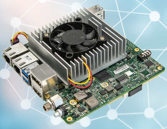
The SBC enables up to 16GB DDR4, 128GB eMMC and offers 4K displays via HDMI, DisplayPort, and eDP. It also features SATA, 2x GbE, 4x USB 3.0, and 40-pin “HAT” and 100-pin GPIO add-on board connectors. Mini-PCIe and dual M.2 slots are available. The dual M 2 slots supports wireless modems and more SATA options, they also support Aaeon’s new AI Core X modules, that offers Intel’s latest Movidius Myriad X VPUs for 1TOPS neural processing acceleration.

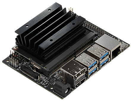
2. Jetson Nano Dev Kit

Nvidia has announced a low-end Jetson Nano compute module which is a smaller (70 x 45mm) version of the old Jetson TX1. It enables 4x Cortex-A57 cores and has a lower-end 128-core Maxwell GPU. The module offers 2GB and 8GB of RAM and flash. It supports 4K video and the GPU offers similar CUDA-X deep learning. It costs $99, supported by a forum and other community resources. It has 40-pin GPIO, an M.2 slot, GbE with Power-over-Ethernet, HDMI 2.0 and eDP links, and 4x USB 3.0 ports.
3. Coral Dev Board

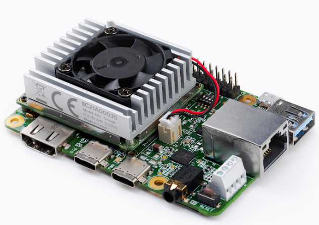
Earlier this month, Google announced its first Linux maker board which features an NXP i.MX8M and Google’s Edge TPU AI chip. The Raspberry Pi-like Coral Dev Board was accompanied by an Edge TPU-enabled Coral USB Accelerator USB stick, then will be followed by an Edge TPU based Coral PCIe Accelerator and a Coral SOM compute module. The devices come with schematics, community resources, and other open-spec resources. The Board features the Edge TPU chip with NXP’s quad-core, 1.5GHz Cortex-A53 i.MX8M, a 3D Vivante GPU/VPU and a Cortex-M4 MCU. The Board offers 4K-ready GbE, HDMI 2.0a, 4-lane MIPI-DSI and CSI, and USB 3.0 host and Type-C ports.
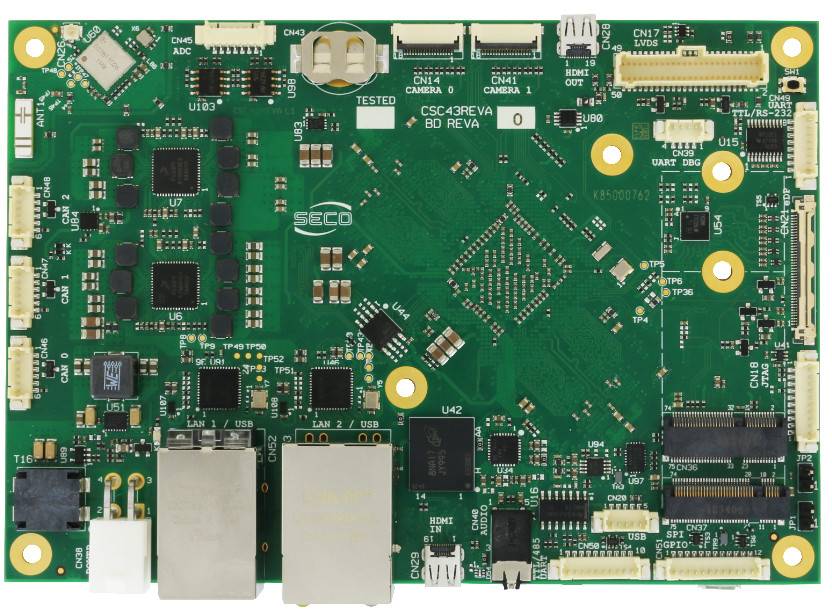
4. SBC-C43

Seco’s SBC-C43 board is the pioneer SBC based on NXP’s high-end, up to hexa-core i.MX8. The SBC supports the i.MX8 QuadMax with 2x Cortex-A72 cores and 4x Cortex-A53 cores, the QuadPlus has a single Cortex-A72 and 4x -A53, and the Quad has no -A72 cores and 4x -A53. The SBC-C43 enables up to 8GB DDR4 and 32GB eMMC. It features dual GbE, HDMI 2.0a in and out ports, WiFi/Bluetooth, and a series of industrial interfaces. Its dual M.2 slots enable SATA, wireless, and more.
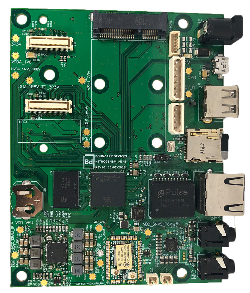
5. Nitrogen8M_Mini

The open-spec Nitrogen8M_Mini from Boundary Device is the first SBC to feature NXP’s new i.MX8M Mini SoC. The Mini utilizes a more advanced 14LPC FinFET process than the i.MX8M, which results in lower power consumption and higher clock rates for both the 4x Cortex-A53 (1.5GHz to 2GHz) and Cortex-M4 (400MHz) cores. With Linux and Android support, the Nitrogen8M_Mini ships with 2GB to 4GB LPDDR4 RAM and 8GB to 128GB eMMC. Its MIPI-DSI and -CSI interfaces support optional touchscreens and cameras, respectively. It offers a GbE port, and PoE and WiFi/BT are optional. It also features 3x USB ports, one or two PCIe slots, and optional -40 to 85°C support. It is available for $135, and shipping due this spring.
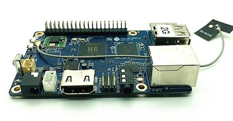
6. Pine H64 Model B

Pine64’s latest hacker board, is part of an open source product, which also includes a laptop, tablet, and phone. Recently going on sale for $39 (2GB) or $49 (3GB), the Raspberry Pi semi-clone composes of the high-end, but low-cost Allwinner H64. The quad -A53 SoC offers 4K video with HDR support.

The Model B enables up to 128GB eMMC storage, WiFi/BT, and a GbE port. I/O features includes 2x USB 2.0 and single USB 3.0 and HDMI 2.0a ports plus SPDIF audio and an RPi-like 40-pin connector.
7. AI-ML Board

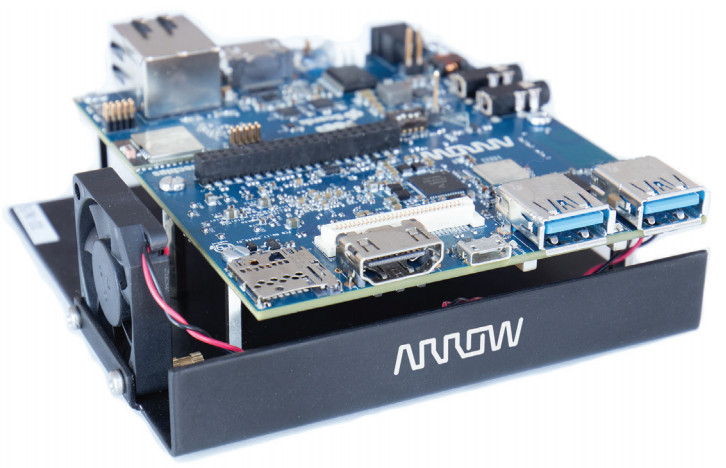
Arrow announced the i.MX8X based SBC earlier this month along side a similarly 96Boards CE Extended format, i.MX8M based Thor96 SBC. The AI-ML Board seems to be the first SBC that features the low-power i.MX8X, which enables up to 4x 64-bit, 1.2GHz Cortex-A35 cores, a 4-shader, 4K-ready Vivante GPU/VPU, a Cortex-M4F chip, and a Tensilica HiFi 4 DSP.

The board offers 2GB LPDDR4, Ethernet, WiFi/BT, and a pair each of MIPI-DSI and USB 3.0 ports. It is expected to launch by June 1.
8. BeagleBone AI

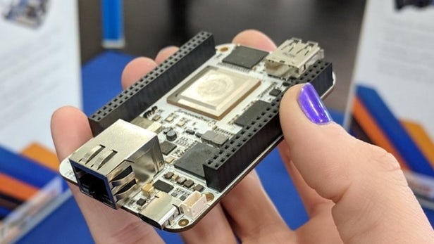
The AI is enabled by dual TI C66x DSPs and four embedded-vision-engine (EVE) neural processing cores. BeagleBoard.org claims that calculations for computer-vision models using EVE run at 8x times the performance per watt compared to the similar, but EVE-less, AM5728. The EVE and DSP chips are supported through a TIDL machine learning OpenCL API and pre-installed tools. The AI is based closely on the BeagleBone Black and offers backward header, mechanical, and software compatibility. It offers 1GB RAM and 16GB eMMC storage. It is due to go on sale for $100 in April.
9. Robotics RB3 Platform (DragonBoard 845c)

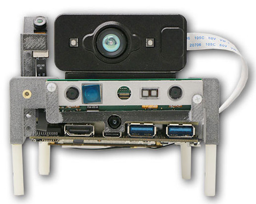
The 10nm, octa-core, “Kryo” based Snapdragon 845 is one of the most powerful Arm SoCs available. It features an advanced Adreno 630 GPU with “eXtended Reality” (XR) VR technology and a Hexagon 685 DSP with a third-gen Neural Processing Engine (NPE) for AI applications. The $449 and up kit features the board’s expansion connectors, which are pre-stocked with Qualcomm cellular and robotics camera mezzanines. The kit also includes standard 4K video and tracking cameras, with optional Time-of-Flight (ToF) and stereo SLM camera depth cameras. The SBC runs Linux with ROS (Robot Operating System).
10. Avenger96

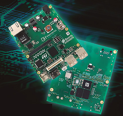
The Avenger96 is a 96Boards CE Extended SBC designed for low-power IoT applications. However, the SBC features a more power-efficient, but slower SoC (ST’s recently announced STM32MP153). The Avenger96 has dual, 650MHz Cortex-A7 cores, a Cortex-M4, and a Vivante 3D GPU.

The board features an Avenger96 module with the STM32MP157 SoC and offers 1GB of DDR3L, 2MB SPI flash, and a power management IC. The Avenger96 SBC is equipped with GbE, HDMI, micro-USB OTG, and dual USB 2.0 host ports. Available also is a microSD slot, and 40- and 60-pin GPIO connectors. The board is expected to go on sale in April.
For further information visit Linux.com
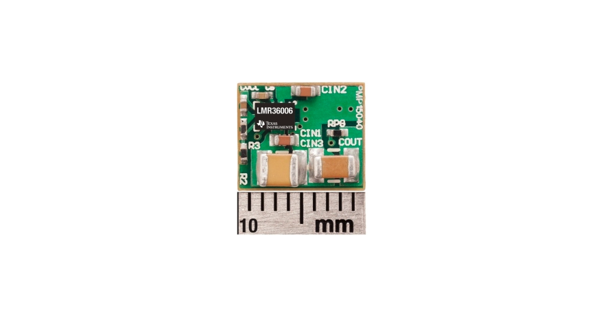
LMR36015 – 4.2-V to 60-V, 1.5-A ultra-small synchronous step-down converter

The LMR36015 regulator is an easy-to-use, synchronous, step-down DC/DC converter. With integrated high-side and low-side power MOSFETs, up to 1.5 A of output current is delivered over a wide input voltage range of 4.2 V to 60 V. Tolerance goes up to 66 V. The transient tolerance reduces the necessary design effort to protect against overvoltages and meets the surge immunity requirements of IEC 61000-4-5.

The LMR36015 uses peak-current-mode control to provide optimal efficiency and output voltage accuracy. Load transient performance is improved with FPWM feature in the 1-MHz regulator. Precision enable gives flexibility by enabling a direct connection to the wide input voltage or precise control over device start-up and shutdown. The power-good flag, with built-in filtering and delay, offers a true indication of system status eliminating the requirement for an external supervisor.

The LMR36015 is in a HotRod™ package which enables low noise, higher efficiency, and the smallest package to die ratio. The device requires few external components and has a pinout designed for simple PCB layout. The small solution size and feature set of the LMR36015 are designed to simplify implementation for a wide range of end equipment, including space critical applications of ultra-small field transmitters and vision sensors.

Features


  • Designed for reliable and rugged applications
    • Input transient protection up to 66 V
    • Junction temperature range –40°C to +150°C
    • Protection features: thermal shutdown, input undervoltage lockout, cycle-by-cycle current limit, hiccup short-circuit protection
    • HotRod™ package enables low noise and minimized switch node ringing
    • 0.4-V dropout with 1.5-A load (typical)
  • Suited for scalable industrial power supplies
    • Pin compatible With:
    • 400-kHz, 1-MHz Frequency options
    • Low power dissipation across load spectrum
      • 90% efficiency at 400 kHz (24VIN, 5VOUT, 1A)
      • 93% efficiency at 400 kHz (12VIN, 5VOUT, 1A)
      • Increased light load efficiency in PFM
      • Low operating quiescent current of 26 µA
    • Small 2-mm × 3-mm HotRod™ package
    • solution with few external components

more information: http://www.ti.com/product/LMR36015

HS101: A high quality, and Cheap DIY Oscilloscope

HS101 Demo

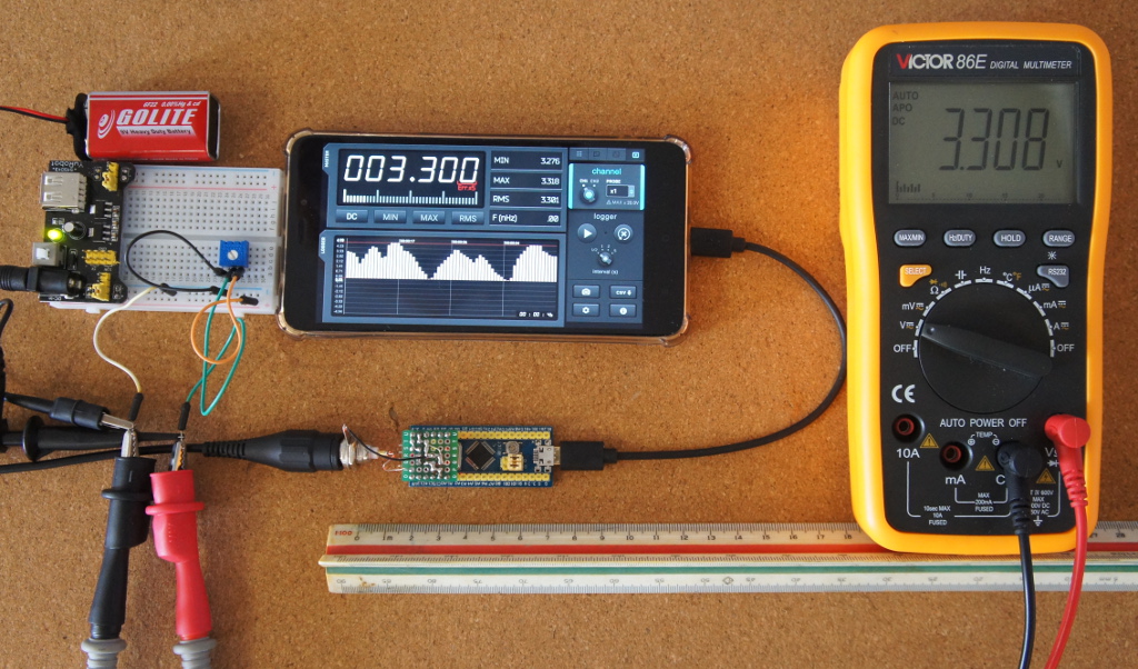
The Oscilloscope is a test instrument used for the visualization and observation of varying signal voltages, usually as a two-dimensional plot with one or more signals plotted against time. They are used in the design and debugging of electronic devices to view and compare waveforms, determine voltage levels, frequency, noise and other parameters of signals applied at its input as it changes with time. This makes Oscilloscopes a very important tool on the desk of an electronics engineer or maker. However, Oscilloscopes are quite expensive, they cost between $45 – $100 for a small oscilloscope and above $300 for advanced oscilloscopes, which puts them beyond the reach of basic users. But what if we could create something cheaper, compact, and highly functional using the components familiar to makers? That is the question that led to today’s tutorial.

For today’s tutorial, we will build the HS101 Oscilloscope. The HS101 Oscilloscope setup comprises of the HS101 portable and compact DIY oscilloscope, connected to an Android-based mobile phone or tablet running the HScope app.  The oscilloscope is based on the STM32F103 microcontroller which has 2 fast, 12-bits ADC and it samples the signal to be examined (after it has passed  condition elements, like a network of resistors capacitors and diodes) on board.

HS101: A high quality, and Cheap DIY Oscilloscope – [Link]

TOP PCB Companies