New Artix-7 FPGA Board with M.2 Interface Fits in a Laptop

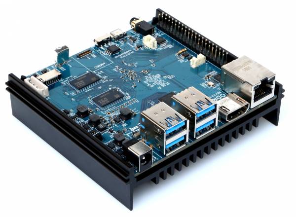
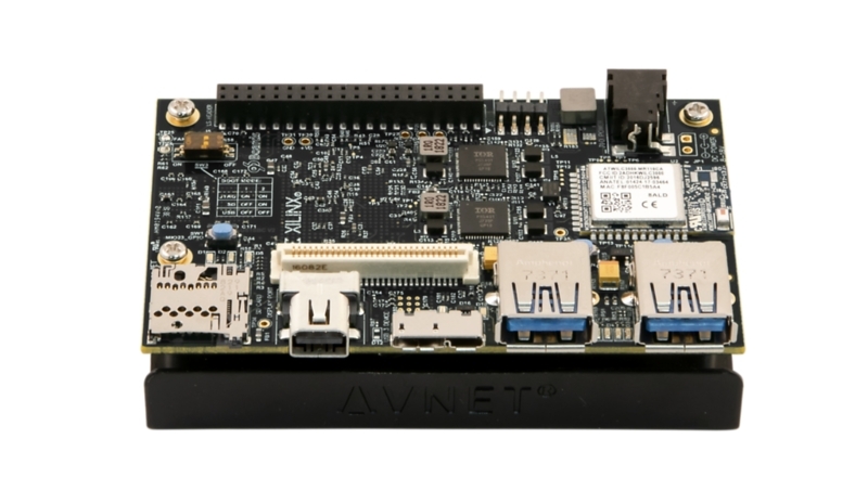
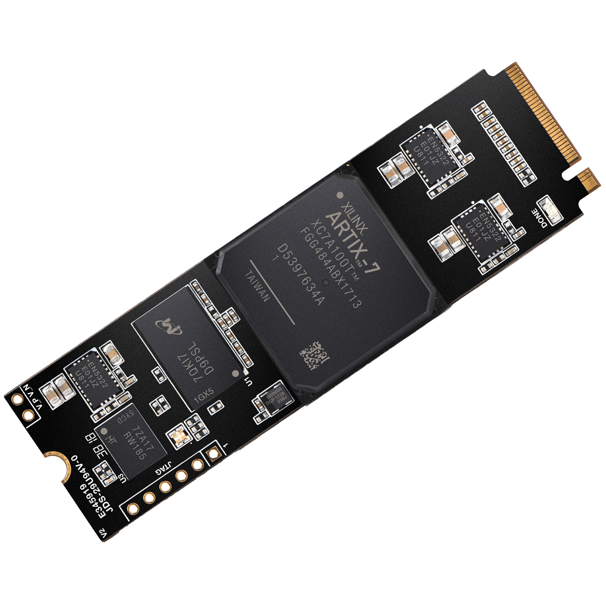
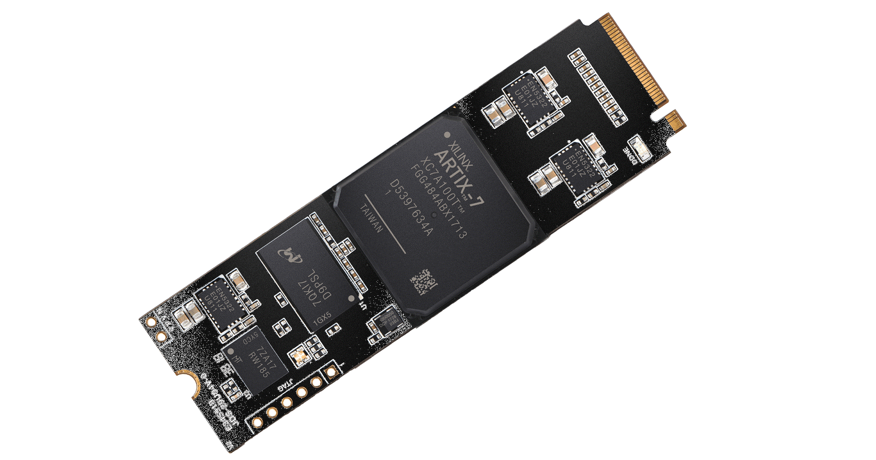
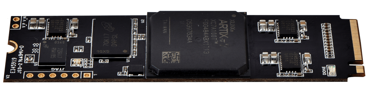
The Aller board is specifically designed for development and integration of FPGA based accelerated features into other larger designs, it can be used with laptops, desktops, and servers featuring standard 2280 M.2 form factor M-key slot.

Nowadays, most of the new laptops come with M.2 M-key slots for NVMe storage modules and Aller can be seamlessly used with those slots. Open source PCI Express IP cores such as litepcie make the development of PCIe designs very cost-effective.

According to Rohit Sigh, Head of Development at the FPGA Division of Numato Lab, Aller was designed to help users with easier access to flexible and reconfigurable PCI Express infrastructure. With the decline of standard PCs and proliferation of M.2 connectors in Laptops, Servers and Desktop PCs, Aller breaks the barrier to PCI Express designs. Aller can also be used with standard PCI Express slots using M.2-to-PCI Express Adapter without any loss of functionality.

Aller is targeted for the users who want to experiment with PCI Express based FPGA designs using simple and cost-effective hardware. But this does not limit the usage of Aller. It can be used for a variety of PCIe acceleration applications.

The board features a Xilinx Artix-7 100T FPGA, the second-most powerful FPGA in the Artix-7 family. Xilinx FPGAs are at the forefront of the FPGA technology and are the most widely used FPGAs globally. The competitive pricing of Artix-7 puts Aller in the category of affordable PCI Express boards.

Features

  • Device: Xilinx Artix 7 FPGA (XC7A100T-1FGG484C)
  • DDR3: 2Gb DDR3 ( MT41J128M16JT-125:K TR )
  • 4 lane PCIe Gen1 (2.5GT/s)
  • Onboard 1Gb QSPI flash memory for FPGA configuration
  • JTAG header for programming and debugging
  • 100 MHZ CMOS oscillator
  • 1 x Trusted Platform Module (AT97SC3205)
  • M.2 Connector Interface, M-Key
  • Powered from M.2 connector
  • 1 RGB LED for custom use

The Artix-7 100T FPGA features ~101K LUTs, ~126K Flip-flops, ~600KiB Block RAM and 240 DSP slices making it very suitable for acceleration applications.

The compact M-key M.2 form-factor provides Aller with a vast number of motherboards and laptops as possible hosts. Most new systems these days ship with an M.2 M-key slot meant for SSDs. So Aller can directly leverage the huge ecosystem of the motherboards. As opposed to A, B or E-keys, the M-key is more common thanks to the SSD popularity and also sports 4x more PCI Express lanes. Since M-key M.2 form-factor supports PCI Express x4, it results in maximum theoretical bandwidth of 1GB/s between Aller and host system, i.e, four times more than competing products.

Featuring an onboard Trusted Platform Module (TPM) IC means Aller users can completely offload their security sensitive computations to the FPGA. TPM helps in secure management of cryptographic keys.

Applications

  • Product Prototype Development
  • Accelerated computing integration
  • Development and testing of custom embedded processors
  • Signal Processing
  • Memory Intensive FPGA development
  • Educational tool for Schools and Universities
  • High Hash Rate calculations for Blockchain technologies such as Bitcoin and Ethereum
  • Offloading computationally intensive algorithms to FPGA
  • Machine Learning and Artificial Intelligence

Aller is a perfect match for several applications such as hardware accelerators, machine learning, and neural network engines, high hash-rate calculations for blockchain technologies, PCI Express kernel driver development training, digital signal processing, and development and testing of embedded processors.

The board is available for purchase at their online store for an introductory price of $399.95 per unit with volume discounts available on request.

For more information, or to purchase Numato Lab products, please visit https://numato.com/ or you can also contact them directly via email at help@numato.com or by phone at 720-513-2210.

High Precision Solder Paste Stencil Printer

This is the most traditional size and classic high precision Solder Paste Stencil Printer for PCBs. The platform can be rotated 30 degrees at most, and the precision can be kept all the way when repeat works. Easy to locate PCB board, high flexibility ensure high printing precision.The brackets using the bolt bar to adjust the height, convenient for controlling the thickness of PCB.
Note, Stencil plate and frame is customized for your own PCBs which is Not included. The picture is only for reference. The solder paste stencil printer starting at $309 with additional accessories available.

Technical Parameters

  • Overall Dimensions(L*W*H) 580*320*259(mm)
  • Platform Size 300*400(mm)
  • PCB Size 270*370(mm)
  • Stencil Size 370*470(mm)
  • Platform Height 180mm
  • PCB Positioning Mode Outside/ Reference Hole
  • Weight 12.7kg

Introduction to Classic 3040 Solder Stencil Printer

This post is a contribution of www.robotdigg.com. RobotDigg offers motorized and linear Delta Robots, Cartesian XYZ, SCARA, SLA 3D Printer, Benchtop Surface Mount, CNC Laser, Robotics and many more products.

Win a Texas Instruments Evaluation Module!

Presenting the Texas Instruments Evaluation Module Giveaway

Here’s your chance to take home a Texas Instruments DUAL-DIYAMP-EVM. This “break apart” EVM has several popular op-amp configurations, including amplifiers, filters, stability compensation and other signal conditioning circuits that require two amplifiers. Build anything from a simple amplifier to complex signal chains by combining different configurations. To enter the giveaway, you must subscribe or be a current subscriber to our newsletters covering the newest products and latest applications. But hurry, the giveaway ends March 31st, 2019.

You just need to SUBSCRIBE or be a current subscriber to Mouser newsletters covering the newest products and latest applications to enter.

Texas Instruments DUAL-DIYAMP-EVM

The DUAL-DIYAMP-EVM is an EVM developed for dual package op amps to give users the ability to easily evaluate amplifier circuits.

Keep in mind, the giveaway ends March 31st, 2019.  View official rules »

Seco “SBC-C43” Module Features Cortex-A72 enabled i.MX8.

Seco is developing a 3.5-inch “SBC-C43”, which runs Linux or Android on an up to hexa-core i.MX8, offering up to 8GB soldered DDR4 and 32GB eMMC plus WiFi/BT, 2x GbE, 3x USB, HDMI 2.0 in and out, 2x M.2, and -40 to 85°C support. Seco’s 3.5-inch SBC enables soldered memory and optional industrial temperature support. It’s built to support medical devices, digital signage, edge computing, industrial automation, IoT, smart vision, and vending.

There has been a host of compute modules based on the Cortex-A72 enabled i.MX8, like the Variscite’s VAR-SOM-MX8 and SPEAR-MX8, but Seco’s 3.5-inch SBC-C43, is the first SBC we have come a-cross to feature the Cortex-A72 enabled i.MX8. The Seco SBC-C43 enables NXP’s default Yocto Project Linux stack and also Wind River Linux and Android.

SBC-C43 back view

The SBC supports all three variants of i.MX8, inclusive of the QuadMax with 2x Cortex-A72 cores and 4x Cortex-A53 cores, the QuadPlus which features a single Cortex-A72 and 4x -A53, and the Quad with no -A72 cores and 4x -A53. The clock rates were not listed but judging from Toradex’s Apalis iMX8 module that clocks the -A72 cores at 1.6GHz and the -A53 cores at 1.26GHz, we can say the SBC-C43 will clocked within that range. The three models also feature 2x Cortex-M4F real-time cores as well as 2x Vivante GPU/VPU cores.

The QuadMax incorporates the GC7000XSVX GPU, but the other two models have the Lite version. The video support is the same, but with 4K30 decoding and the capacity to drive up to 4x displays simultaneously. However, the 4K resolution is being shared between the different outputs. The SBC-C43 enables up to 8GB DDR4 and up to 32GB eMMC, which are soldered to the board for a greater durability.

SBC-C43 block diagram

Available also are, a boot flash, a microSD slot, and SATA support through its M.2 Key B slot, which otherwise can load a modem card or other M.2 PCIe add-ons. Media I/O options offers HDMI 2.0a output and input ports, an optional eDP connector, and dual-channel LVDS. The SBC-C43 is further equipped with 4-lane MIPI-CSI, and an audio I/O connector. It offers a USB 3.0 and 2.0 host port and also a micro-USB 2.0 OTG port. Internal I/O features includes 2x USB, 3x serial, 3x CAN, and 6x GPIO. A non-storage ready M.2 Key E slot, and a SIM card slot are available on the module. The SBC offers 2x GbE ports, a WiFi 5 (ac) with Bluetooth module plus internal antennas.

Specifications listed for the SBC-C43 include:

  • Processor — NXP i.MX8 with VPU with H.265 (4K30) and H.264 (1080p60) decoding and H.264 (1080p30) encoding:
  • i.MX 8QuadMax — 2x Cortex-A72, 4x Cortex-A53, 2x Cortex-M4F, 2x Vivante GC7000 / XVSX GPU/VPU
  • i.MX 8QuadPlus — 1x Cortex-A72, 4x Cortex-A53, 2x Cortex-M4F, 2x GC7000Lite / XVSX GPU/VPU
  • i.MX 8Quad — 4x Cortex-A53, 2x Cortex-M4F, 2x GC7000Lite / XVSX GPU/VPU
  • Memory/storage: 2GB, 4GB, 6GB, or 8GB soldered, 1600MHz DDR4, 4MB Quad SPI NAND flash (boot only)
  • Up to 32GB soldered eMMC 5.1, MicroSD slot, SATA via M.2 Key B (see expansion below)
  • Networking/wireless: 2x GbE ports, 802.11 a/b/g/n/ac + BT LE 4.2 module with ceramic SMT antennas, M.2 slots (see expansion below)
  • Media I/O: HDMI 2.0a output port up to 4K, HDMI 2.0a input port, Optional eDP to 4K, Dual-channel 18/24-bit LVDS up to 1080p, Quadruple display support, 2x 4-lane MIPI-CSI, I2S audio codec, Mic-in, line-out via single combo TRRS connector
  • Other I/O: USB 3.0 host port, USB 2.0 host port, Micro-USB 2.0 OTG port, USB 2.0 header plus up to 2x more via M.2 slots, 3x UARTs (RS-485/RS-422, RS-232, TTL), 3x CAN, 6x GPIO, 4x analog inputs, SPI, I2C
  • Expansion: M.2 Key E for PCIe/USB wireless, etc., M.2 Key B for SATA, PCI-e x1, etc. (see memory/storage above), SIM slot
  • Other features — RTC
  • Power — 12VDC input
  • Operating temperature — 0 to or 60°C or -40 to 85°C
  • Dimensions — 146 x 102mm (3.5-inch)
  • Operating system — Yocto, Wind River Linux, Android

More information can be found on Seco’s SBC-C43 product page.

Allwinner H5 SBC is loaded with WiFi, BT, LTE, GPS, and triple CSI

Introducing one of the smallest, most upgrade-able, most complete SBC’s on the market sporting the Allwinner H5, the Prime Series 1. The H5 Quad Core SOM (System on a Module) in our dev kit is perfect for makers and developers.

The SOM Module is loaded with features and the complete kit makes those features easier to access. The system is powered by a 64-bit ARM Cortex-A53 and a ARM Mali 450 MPR GPU. It has 512MB of RAM and 8GB eMMC storage. We found it hard to find a board with support for greater than one (1) MIPI/CSI camera so we included three (3) mipi csi camera ports. This means no multiplexed cameras or additional hardware to provide 360 degrees visibility. For connectivity, we found most systems only had Wi-Fi/Bluetooth or it was an add-on, so there are a plethora of wired and wireless options available. For wireless needs, the system rocks an Atheros 802.11 b/g/n and Bluetooth 4.0 dual-mode BLE all with the built-in antenna, and a GSM/LTE Global services modem with GPS/GLONASS.

Prime Series 1, front


Prime Series 1, back

The development board also adds a MicroSD slot for more storage, a 10/100 Ethernet port; so whether wired and/or wireless, we have you covered. The SOM module itself is upgradable, and in our future plans we will release more configurations. Right now it is 512MB, 8GB Emmc. The board itself has GPIO, HDMI, Audio In/Out, Dual USB Type-C, and a USB OTG.

Specifications listed for the Prime Series 1 include:

  • Processor (via H5 Quad Core SOM) — Allwinner H5 (4x 64-bit Cortex-A53 cores @ 400MHz to 1.4GHz) with Mali-450 MP4 GPU; ATECC508A Secure Element
  • Memory/storage:
    • 512MB DDR3 RAM (via H5 Quad Core SOM)
    • 8GB eMMC (via H5 Quad Core SOM)
    • MicroSD slot
  • Networking/wireless:
    • 10/100 Ethernet port
    • Atheros 802.11b/g/n with Bluetooth 4.0 dual-mode BLE (via H5 Quad Core SOM)
    • GSM/LTE global services modem with GPS/GLONASS
    • Internal ceramic antenna
    • Optional U.FL external antenna
  • Media I/O:
    • HDMI port
    • 3x MIPI-CSI
    • 3.5mm audio in and out jacks
    • I2S/PCM header
  • Other I/O:
    • USB 2.0 OTG port
    • 2x USB Type-C ports
    • 5x UART
    • 2x SPI
    • 4x I2C
    • 1x SDIO
    • 2x PWM
    • 60x GPIO
  • Other features — IR receiver; heatsink; micro-USB to USB cables; 2x DF40 80-pin B-to-B connectors to SOM
  • Operating temperature — -20 to 70°C
  • Power — VDD-IO: 3.3 V; Core: 1.1-1.3 V
  • Dimensions — 85 x 55mm
  • Operating system — Images for Yocto project (default); Ubuntu, Android, Windows Embedded ARM, and FreeBSD; optional Uptane OTA (also supports Mender, Balena, and OSTree

In today’s environment, we can’t forget about security. The system comes with the ATECC508A Secure Element for storing cryptographic keys, unique IDs, and supports the creation of FIPS random numbers. So you can provide crypto based security. You only find this in add-on boards from other vendors, and we understand today’s needs so we included it by default.

The Prime Series 1 will go on pre-order for $175 on GroupGets on Mar. 29. No ship date was mentioned, but the website states:

The Prime Series 1 is ready to be ordered, manufactured, and shipped to your destination.

More information on the Prime Series 1, including a link to the GroupGets page, is available on the Optimus Embedded website.

First COM Express Type 7 Module with Intel Atom C3000 Processor

MSC Technologies Presents First COM Express Type 7 Module with Intel Atom C3000 Processor for Server Applications

Stutensee, Germany – MSC Technologies, the technology brand of Avnet Integrated Solutions, presents the MSC C7B-DV, its first COM Express™ module in accordance with the new Type 7 standard, at the embedded world 2018 in Hall 2, Booth 238. COM Express™ Type 7 was introduced in the current COM.0 Rev. 3.0 specification of the PICMG (PCI Industrial Computer Manufacturers Group).

The MSC C7B-DV COM Express™ Type 7 module is equipped with a powerful Intel® Atom™ C3000 series server processor (“Denverton”) and is especially designed for applications where large amounts of data are processed and transferred at high bandwidths. Such applications include edge servers, content servers, Wi-Fi routers in public transportation and image or video processing systems in industry and healthcare. For use in harsh environmental conditions, individual module variants are also specified for the industrial temperature range from -40°C to +85°C. The computer-on-module will be available for at least fifteen years from the product launch of the processor.

The modules can be equipped with seven different Intel® Atom™ server processors, offering broad scalability from four to sixteen processor cores. Relatively inexpensive entry-level models are also available. Via two 260-pin SO-DIMM sockets, the module can be equipped with fast DDR4 SDRAMs with a maximum capacity of 48 GB, optionally with Error Correction Code (ECC). The integrated Infineon Trusted Platform Module TPM 2.0 provides additional security for critical network installations.

Up to five Ethernet interfaces, four with 10Gb and one connection with 1Gb transfer rate, provide high network bandwidth. Up to 22 PCI Express™ (PCIe) lanes enable flexible system expansions and the connection of fast SSD memory. In addition, there are two SATA 6Gb/s interfaces, three USB 3.0 ports, four USB 2.0 and two serial high-speed connections.

To evaluate the MSC C7B-DV family of server modules, MSC Technologies supplies a matching Type 7 carrier board in ATX form factor and a comprehensive starter kit. In addition to numerous interfaces and PCIe slots, the carrier board can optionally be provided with a Board Management Controller (BMC) that supports out-of-band management.

An MSC C7-MB-EV Type 7 carrier board is available for evaluation. The 0 to 85°C tolerant, 305 x 244mm ATX board is equipped with an SD slot, dual SATA III sockets, 4x USB 3.0 ports, and 4x serial headers.

No pricing or availability information was provided for the MSC C7B-DV module. More information may be found in MSC’s MSC C7B-DV announcement and product page.

Qualcomm Unveils Snapdragon 855 Hardware Development Kit (HDK)

Snapdragon 855 is a popular, high-end processor that is found in premium smartphones such as Samsung Galaxy S10 or Xiaomi Mi 9. Recently Snapdragon 855 Mobile Hardware Development Kit appeared on Qualcomm developer website. The Qualcomm® Snapdragon™ 855 mobile hardware development kit (HDK) is a highly integrated and optimized Android development platform designed for technology companies to integrate and innovate mobile device development on the Snapdragon 855 mobile platform.

Snapdragon 855 is a octa-core processor fabricated with 7nm process and comes with WiFi 5, Bluetooth 5.0, GNSS, Gigabit Ethernet, multiple MIPI DSI and CSI interfaces, DisplayPort over USB-C and HDMI outputs and more.

Snapdragon 855 HDK preliminary specifications:

  • SoC –  Qualcomm Snapdragon 855 Octa-core processor with 1x Kryo 485 Gold Prime core at up to 2.8 GHz, 3x Kryo 485 Gold cores at up to 2.4 GHz, and 4x Kryo 485 Silver low-power cores at up to 1.7 GHz, Adreno 640 GPU
  • System Memory – TBD
  • Storage – TBD flash, micro SD card slot
  • Video Output
    • 2x MIPI 4-lane DSI + touch panel
    • 1x HDMI
    • DisplayPort over USB 3.1 type-C port
  • Camera Input – 3x MIPI 4-lane CSI with support for 3D camera configuration
  • Connectivity
    • Gigabit Ethernet
    • WiFi 5 802.11ac 2×2 with MU-MIMO; “WiFi 6 ready”
    • Bluetooth 5.0
    • GNSS  – GPS/GLONASS/COMPASS/GALILEO
  • USB – 2x USB 3.0 type A ports, 1x USB 3.1 type-C port
  • Expansion
    • 2x Sensor I/O connectors
    • Audio input and output header
    • 3.5mm audio headset jack
    • Mini PCIe port
    • 96boards? HS and LS connectors
    • VERTIGO connector (what is it for?)
  • Debugging – 1x micro USB port
  • Misc – 4x user LEDs, WiFi and Bluetooth LEDs, power and volume buttons
  • Power Supply – 12V DC via power barrel, and maybe USB-C port
  • Dimensions – Not specified, but it sure looks like the board follows 96Boards CE Extended specs, so it should be 100×85 mm

The board supports Android 9, and the company provides optional accessories including a 5.7″ touchscreen display with 2560×1440 resolution and expansion board, as well as camera modules, namely 12MP + 5MP front camera, and DUAL 12MP + 13MP rear cameras.

Snapdragon 855 HDK shown with optional LCD display

There is no information accessible on availability and pricing and possibly it should be sold by Intrinsyc with a price tag well over $1,000 without accessories, since Snapdragon 845 HDK already sells for $1,079.

Odroid-N2 SBC launches at $63 with new Cortex-A73 SoC

ODROID-N2 is a new generation single board computer that is more powerful, more stable, and faster performing than ODROID-N1. The main CPU of the N2 is based on big.Little architecture which integrates a quad-core ARM Cortex-A73 CPU cluster and a dual core Cortex-A53 cluster with a new generation Mali-G52 GPU. Thanks to the modern 12nm silicon technology, the A73 cores runs at 1.8Ghz without thermal throttling using the stock metal-housing heatsink allowing a robust and quiet computer.

The CPU multi-core performance is around 20% faster and the 4GByte DDR4 RAM is 35% faster than the N1. The N2’s DDR4 RAM is running at 1320Mhz while N1’s DDR3 was running at 800Mhz. The large metal housing heatsink is designed to optimize the CPU and RAM heat dissipation and minimize throttling. The CPU is placed on the bottom side of the PCB to establish great thermal characteristics.

ODROID-N2 block diagram

The specs for the Odroid-N2 appear to be the same as those we detailed in February when the SBC was formally announced.

Specifications listed for the Odroid-N2 include:

  • Processor — Amlogic S922X (4x Cortex-A73 @ 1.8GHz, 2x Cortex-A53 @ 1.9GHz); 12nm fab; Mali-G52 GPU with 6x 846MHz EEs
  • Memory/storage:
    • 2GB or 4GB DDR4 (1320MHz, 2640MT/s) 32-bit RAM
    • eMMC socket with optional 8GB to 128GB
    • MicroSD slot with UHS-1 SDR104 support
    • 8MB SPI flash with boot select switch and Petitboot app
  • Wireless — Optional USB WiFi adapter
  • Networking — Gigabit Ethernet port (Realtek RTL8211F); about 1Gbps
  • Media I/O:
    • HDMI 2.1 port for up to 4K@60Hz with HDR, CEC, EDID
    • Composite video jack with stereo line-out and 384Khz/32bit audio DAC
    • SPDIF audio via 40-pin
  • Other I/O:
    • 4x USB 3.0 host ports (340MB/s typical)
    • Micro-USB 2.0 OTG port (no power)
    • Serial console interface
    • Fan connector
  • Expansion — 40-pin GPIO header (25x GPIO, 2x i2C, 2x ADC, 6x PWM, SPI, UART, SPDIF, various power signals, etc.)
  • Other features — RTC (NXP PCF8563) with battery connector; IR receiver; metal heatsink; 2x LEDs; optional $4 acrylic case
  • Power — 7.5-20V DC jack; 12V/2A adapter recommended; consumption: 1.8W idle to 5.5W stress
  • Dimensions — 90 x 90 x 17mm
  • Operating system — Ubuntu 18.04 LTS with Kernel 4.9.152 LTS and Android 9 Pie BSPs

The Odroid-N2 is on sale for $63 (2GB RAM) or $79 (4GB) with shipments beginning April 3. More information may be found on Hardkernel’s $63 (2GB RAM) and $79 (4GB) shopping pages and the Odroid-N2 wiki.

Avnet Introduces Ultra96-V2 Development Board with certified WiFi

Just one year after introducing its successful Ultra96 development board, Avnet, a leading global technology solutions provider, has released the new Ultra96-V2 to power industrial-grade Artificial Intelligence (AI) and Internet of Things (IoT) applications. Complete with an updated radio module that enables engineers to extend their reach into new markets, Avnet’s Ultra96-V2 is an ideal platform for smart home, automotive, industrial controls and many other applications.

The Ultra96-V2 board offers engineers and makers a very price competitive development platform for rapidly prototyping the next breakthroughs in AI, IoT, robotics and beyond,” said Bryan Fletcher, technical marketing director, Avnet. “Avnet is proud to support the 96Boards initiative by bringing new performance, additional power-savings, and programmable logic advances to this community of Arm experts and enthusiasts.

The Ultra96-V2 enhances the capabilities of the 96Boards community with a range of peripherals and acceleration engines in the programmable logic not available from other offerings. Like its predecessor, the Ultra96-V2 is an Arm-based, Xilinx Zynq UltraScale+™ MPSoC development board built on the Linaro 96Boards Consumer Edition (CE) specification. The 96Boards are open source development platforms that can be used by system software developers for software applications, hardware devices and kernel programming for operating systems.

Ultra96-V2 block diagram

Engineers can now extend the market reach of their innovations globally with the Ultra96-V2’s new feature – a Wi-Fi / Bluetooth radio module from Microchip that is Agency Certified in more than 75 countries. Wireless options include 802.11b/g/n WiFi and Bluetooth 5 Low Energy support.

The Ultra96-V2 features include:

  • Xilinx Zynq UltraScale+ MPSoC ZU3EG A484
  • Micron 2 GB (512M x32) LPDDR4 Memory
  • Delkin 16 GB microSD card + adapter
  • PetaLinux environment available for download
  • Microchip Wi-Fi / Bluetooth
  • Mini DisplayPort (MiniDP or mDP)
  • 1x USB 3.0 Type Micro-B upstream port
  • 2x USB 3.0, 1x USB 2.0 Type A downstream ports
  • 40-pin 96Boards Low-speed expansion header
  • 60-pin 96Boards High-speed expansion header
  • 85mm x 54mm form factor
  • Linaro 96Boards Consumer Edition compatible

The platform comes as a complete development kit including:

  • Ultra96-V2 development board
  • 16 GB microSD card + adapter
  • Voucher for SDSoC license from Xilinx
  • Quick-start instruction card

Avnet also updated all components on the Ultra96-V2 to allow industrial temperature grade options so that the board can operate in harsh industrial applications. Additional power control and monitoring is also possible with Infineon’s integrated power management ICs (PMICS) designed for tight board space requirements.

Ultra96-V2 allows the 96Boards community members to explore programmable logic to accelerate software. Software engineers’ C, C++, and OpenCL algorithms can be compiled into the FPGA portion of the Zynq UltraScale+ MPSoC to achieve massive parallelism and really high performance,

said Tomas Evensen, CTO of Embedded Software at Xilinx.

The Ultra96-V2 development board will be available in May for $249. More information may be found on Avnet’s Ultra96-V2 product page and shopping page.

Tiny, octa-core Arm module (Qualcomm SDA660) targets AI on the edge

Designed for use in 4K Cameras, Gaming, Digital Signage, and other Consumer and Industrial IoT Devices.

Intrinsyc Technologies Corporation, a leading provider of solutions for the development and production of embedded and Internet of Things (IoT) products, today announced the availability of the Open-Q™ 660 µSOM (micro System on Module) and Development Kit.

Intrinsyc’s Open-Q™ 660 µSOM is an ultra-compact (50mm x 25mm) production-ready embedded computing module.  The SOM is powered by the Qualcomm® SDA660 system on chip (SoC), a product of Qualcomm Technologies, Inc., and is designed to support high-performance, intelligent, on-device processes utilizing heterogenous compute capabilities to power a variety of high-performance consumer and industrial IoT devices.

Open-Q 660 μSOM, back
Open-Q 660 μSOM, front

The Qualcomm SDA660 features eight Qualcomm® Kryo™ 64-bit 260 cores that are divided in two clusters – a fast cluster of four cores with up to 2.2 GHz and a power saving efficiency cluster of four cores with up to 1.8 GHz. Additional high-end features in Qualcomm SDA660 mobile platform include the powerful Qualcomm® Artificial Intelligence (AI) Engine), Qualcomm Spectra™ ISP, and Qualcomm® Hexagon™ 680 DSP with Hexagon Vector eXtensions (HVX), designed to support Caffe2 and Tensorflow for machine learning and image processing.

Intrinsyc’s Open-Q™ 660 µSOM is an ideal platform to power the growing demand for consumer and industrial IoT devices capable of artificial intelligence and machine learning,” said Cliff Morton, Vice President, Solutions Engineering, Intrinsyc. “To assist with integration of our System on Modules into customer products, Intrinsyc offers strong capabilities in all phases of product development. Services include everything from electrical and mechanical design to software development, including camera and audio tuning, artificial intelligence, power optimization, device management, security, and more.

We are proud to see Intrinsyc’s new micro-SOM product being powered by the Qualcomm SDA660,

said Jeffery Torrance, vice president, business development, Qualcomm Technologies, Inc.

Qualcomm Technologies is driving the Internet of Things forward with our cutting-edge compute and connectivity technologies, and we are honored to enable a bright future of IoT devices along with Intrinsyc.

Open-Q™ 660 µSOM Specifications:

  • Qualcomm® SDA660 SoC:
    • Qualcomm® Kryo™ 260 CPU (up to 2.2GHz)
    • Qualcomm® Adreno™ 512 GPU
    • Qualcomm® Hexagon™ 680 DSP with Hexagon Vector extensions
  • System Memory: eMCP – 4GB LPDDR4x RAM + 32GB eMMC storage
  • Wireless Connectivity: Wi-Fi 802.11a/b/g/n/ac 2.4/5Ghz 2×2 MU-MIMO + Bluetooth 5.x
  • Display Interfaces:
    • 2x MIPI 4-lane DSI + touch panel
    • VESA DisplayPort v1.3 via USB Type-C, up to 4K30 or 2K60
  • Camera Interfaces:
    • 3x MIPI CSI D-PHY1.2 camera ports
    • Dual 14-bit Qualcomm Spectra™ ISP supports up to 2 x 16MP cameras
  • Video Performance:
    • Encode: 4K30 HEVC/H.264/VP8/MPEG4
    • Decode: 4K30 8-bit: H.264/VP8/VP9, 4K30 10-bit: HEVC
    • Concurrent: 1080p60 Decode + 1080p30 Encode
  • Audio Interfaces:
    • SLIMBus to support Qualcomm® WCD9335 audio codec (off-SOM)
    • Multi-channel I2S digital audio interface
  • I/O Interfaces:
    • 1x USB3.1 Gen1 Type C
    • 1x USB 2.0 Host
    • 1x SDIO 4-bit interface
    • General purpose UART, I2C, SPI
    • Sensor interface – SPI, UART, I2C to sensor DSP core
  • Power: Integrated battery management on SOM
  • Size: 50mm x 25mm
  • Operating System: Android 9 Pie

Developement Kit

To help IoT device makers accelerate time to market, Intrinsyc provides the Open-Q™ 660 µSOM Development Kit, as well as turnkey product development services, driver and application software development, technical support, and documentation.

Intrinsyc’s Open-Q 660 µSOM Development Kit is a full-featured development platform including the software tools and accessories required to immediately begin development. The development kit marries the production-ready Open‐Q™ 660 µSOM with a carrier board providing numerous expansion and connectivity options to support the development and testing of a wide variety of peripherals and applications, ensuring the fastest time to market possible. The Development Kit is available for purchase at  https://shop.intrinsyc.com/products/open-q-660-usom-development-kit

The Open-Q 660 µSOM is available for pre-order at $225 in single quantities, with shipments due in April. More information may be found in Intrinyc’s Open-Q 660 µSOM announcement, product page, and shopping page.

TOP PCB Companies