Proper reflow oven maintenance can extend its life cycle, keep the machine in good condition, and improve production efficiency and product quality. One of the most important tasks for properly maintaining a reflow oven is remove the built-up flux residue inside the oven’s chamber. Although there is a flux collection system in modern reflow machines, there still is a big probability that flux will adhere to the inert air ventilation pipe and thermal regulator panel. This will cause inaccurate thermal data readings and the thermal controller will make the wrong adjustment instructions.
The following is a list of daily, house-keeping tasks to be accomplished for maintaining a reflow oven:
Clean and wipe down the machine daily. Make a neat workplace.
Check conveyor chains, sprockets, mesh and the automatic lubrication system. Add lubricate oil on time.
Clean the photoelectric switches which detect whether a board is within or outside of the reflow oven.
Additional maintenance tasks include:
Once the chamber temperature decreases to room temperature, open the hood and clean the inside surface of chamber with a proper cleaning agent.
Clean the ventilation pipe with a cleaning agent.
Vacuum the chamber and remove the flux residue and soldering balls.
Check and clean the air blower.
Check and replace the air filter.
The following table is a typical lubrication schedule example:
Description – Period – Recommended lubricant
Head sprocket, bearings and adjustable chain – Every Month – Calcium-based lubricant ZG-2
Timing chain, bearings, and tension pulley
Guide, mesh, and cylinder bearing
Conveyor bearings
Ball screw
PCB carrier chain – Every day – Dupont Krytox GPL107
Inert ball screw and guider – Every week – Dupont Krytox GPL227
Guider support
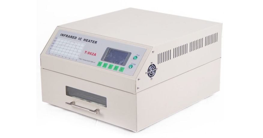
The most popular desktop reflow oven from RobotDigg China
This post is a contribution of www.robotdigg.com. RobotDigg offers motorized and linear Delta Robots, Cartesian XYZ, SCARA, SLA 3D Printer, Benchtop Surface Mount, CNC Laser, Robotics and many more products.
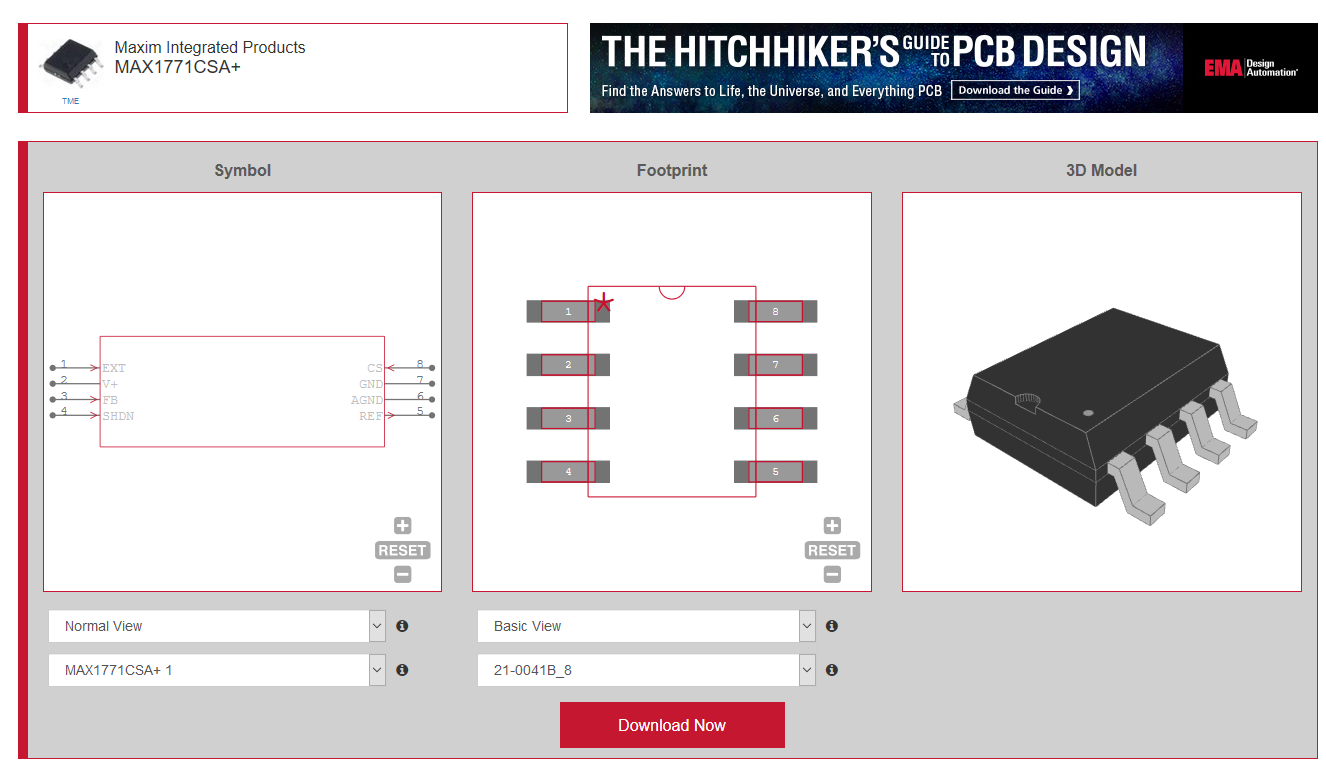
EMA Design Automation has launched its Ultra Librarian Model Cloud on the Maxim Integrated Products website, covering nearly 100% of their parts. By Julien Happich @ eenewseurope.com:
A primary step in creating the electronic design necessary for these solutions is to create or download the symbols, footprints, and 3D models required by the ECAD and MCAD toolsets used by design engineers. The addition of the Ultra Librarian Model Cloud download capability to Maxim’s website combines part research with CAD model download. When a user finds a part for their design, they can examine each of the models in different views and detail levels to confirm their part choice. They can then choose from 29 different CAD formats (including Altium, OrCAD, and SOLIDWORKS), specify preferences on the generated models, and download the ECAD and MCAD models in a seamless online experience.
The models Maxim provides on its website are part of an ongoing collaboration with Ultra Librarian.
The Ultra Librarian team recently created over 7,000 additional part models, verified by both Ultra Librarian and Maxim engineers, bringing the total count to over 85,000 Maxim products. This gives Maxim nearly 100% model coverage for their entire product line. As Maxim creates new products, the Ultra Librarian team will add models into the Ultra Librarian database so Maxim customers can access them from their CAD tool of choice.
To download CAD models from Ultra Librarian’s library of over 15 million parts for free, visit www.ultralibrarian.com.
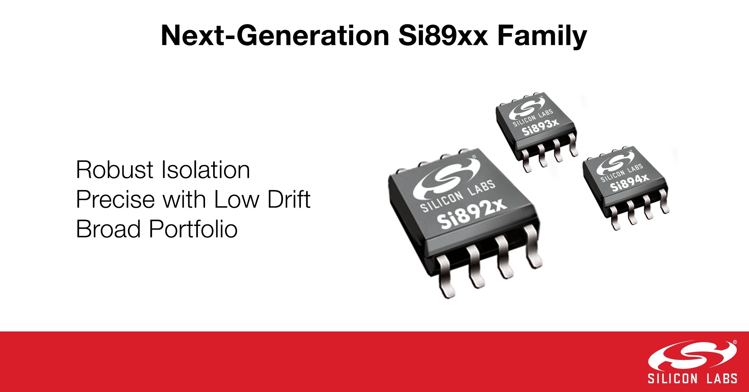
Silicon Labs’ next-generation Si89xx isolated ICs ensure precise current and voltage measurements with ultra-low temperature drift.
Silicon Labs has introduced a family of isolated analog amplifiers, voltage sensors and delta-sigma modulator (DSM) devices designed to provide accurate current and voltage measurement with very low drift across temperature. Based on Silicon Labs’ robust, third-generation isolation technology, the new Si89xx family provides flexible voltage, current, output and package options to help developers reduce BOM cost and shrink board space for a wide range of industrial and green-energy applications including electric vehicle (EV) battery management and charging systems, dc-dc converters, and motor, solar and wind turbine inverters.
Precise current and voltage measurement is essential for accurate operation of power control systems. To maximize efficiency and respond quickly to faults or changes in load, system controllers require current and voltage information from high-voltage rails. Silicon Labs’ third-generation isolation technology keeps controllers safe across wide temperature variations with 1414 V working voltage and 13 kV bipolar surge, exceeding stringent industry requirements.
Silicon Labs now offers the industry’s broadest portfolio of current and voltage sensors. The Si89xx family includes four product categories:
Si892x isolated analog amplifiers optimized for shunt-current sensing
Si8931/2 isolated analog amplifiers optimized for general-purpose voltage sensing
Si8935/6/7 isolated DSM devices optimized for voltage sensing—an industry first
Si8941/6/7 isolated DSM devices optimized for shunt-current sensing
Our first and second generation mixed-signal isolation technologies have driven the strong market success of our digital isolation products over the past decade, and our third-generation technology used in the new Si89xx devices raises the bar even higher,
said Brian Mirkin, Vice President and General Manager of Silicon Labs’ power products.
Our isolation products continue to replace traditional optocouplers and outperform competing digital isolators, enabling higher surge performance, reliability, integration and best-in-class safety for system designs requiring protection from high voltages.
Automotive battery and motor/photovoltaic inverter systems require reliable current monitoring with robust noise immunity. The Si89xx devices provide up to 3x higher common-mode transient immunity (CMTI) than competing products. The devices’ 75 kV/µs immunity to fast transients ensures reliable and accurate current readings in demanding industrial applications. The Si89xx family also supports a fail-safe indication to the host controller if the high-side supply voltage is not detected.
The Si89xx devices provide typical offset error as low as ±40 µV and ±0.1% gain error, enabling precise measurements. Typical offset drift as low as ±0.15 µV/˚C and typical gain drift as low as –6 ppm/˚C ensure exceptional accuracy across temperature. The devices offer the industry’s highest typical signal-to-noise ratio (SNR)—up to 90 dB. A unique low-power mode automatically reduces current draw on one side of the isolation barrier to approximately 1 mA whenever voltage is removed from the other side, enabling a controller to manage power with a simple field-effect transistor (FET).
The next-generation Si89xx devices enhance design flexibility with the following options:
Current or voltage-optimized devices with single-ended, differential or DSM output
±62.5 mV, ±250 mV or 2.5 V input ranges
A stretched wide-body SOIC-8 package to support 5 kVrms isolation and 9 mm creepage/clearance and a compact narrow-body SOIC-8 to support 2.5 kVrms isolation
Pricing and Availability
Advanced samples of Si892x/3x/4x devices in wide-body SOIC-8 packages are available now, and advanced samples of the devices in narrow-body SOIC-8 packages are planned to be available in Q2. Production quantities of all Si89xx devices are planned for Q3. Silicon Labs offers a wide range of evaluation kits to accelerate development. Contact your local Silicon Labs sales representative or authorized distributor for IC and evaluation kit pricing. For more information and to request device samples, visit silabs.com/nextgen-si89xx.
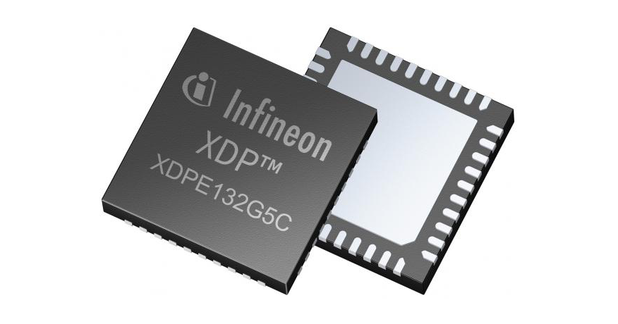
Adding to its high current system chipset portfolio, Infineon claims to offer the industry’s first 16-phase digital PWM multiphase controller.
The XDPE132G5C extends the existing portfolio which enables currents of 500 to 1000A and above for next generation CPUs, GPUs, FPGA and ASICs used in artificial intelligence (AI) and 5G datacomms applications.
It has been introduced as CPU current requirements increase to enable next-generation AI and networking workloads, DC/DC voltage regulators to deliver more than 500A to the load. The XDPE132G5C has a true 16-phase digital PWM engine and an improved advanced transient algorithm to address these high phase count requirements, says Infineon. The true active current sharing between phases enables a reliable, compact and cost-saving design, with no need for extra logic doubler ICs.
The XDPE132G5C offers fine V out setting in 0.625mV increments to meet the demands of ASICs and FPGAs of V out control in less than 1mV steps, seen in communication systems today. The XDPE132G5C also supports auto-restart for communications with options to reduce remote site maintenance following power or system glitches.
The XDPE132G5C is packaged in a 7.0 x 7.0mm 56-pin QFN to accommodate 16 phases. It employs a full digital and programmable load line and is PMBus 1.3/AVS-compliant.
Infineon advises that it can be paired with TDA21475, the thermally efficient integrated current sense power stage, to efficiently deliver over 1000A.
The 70A-rated TDA21475 power stage is housed in a 5.0 x 6.0mm package. It provides efficiency of more than 95 per cent. The exposed top significantly reduces the R th(j-top) from 19 degrees C/W in the over-moulded package to 1.6 degrees C/W. This removes heat from the top of the package, for voltage regulator power density and optimal phase count and footprint. The TDA21475 also offers smart over-current and over-voltage protection and delivers temperature and current information to the XDPE132G5C controller.
The company also offers the IR35223 true 10-phase PWM digital controller. This controller provides a cost-effective option for voltage regulation up to 500 A. The IR35223 is housed in a 6.0 x 6.0mm, 48-pin QFN package and provides advanced transient performance and telemetry features including PMBus 1.3/AVS bus compliance.
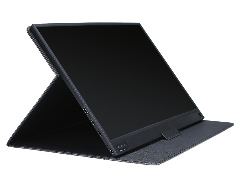
T-bao T15A 15.6″ LCD is a portable display you can connect to your smartphone, game console or computer and enjoy better visibility and usability. It comes with two USB-C ports one for power, one to connect USB-C devices like smartphones, and a mini HDMI port for laptops, computers, game consoles and so on. It can serve as a secondary display for your computer/laptop running Windows 10 or possibly Linux OS or as main screen for your gaming experience.
The display has not it’s own battery so it must be connected to a wall adapter as long as in use and you can even charge your smartphone connected to it.
2x USB type-C ports including one for host device input, one for power
1x micro USB port to connect keyboard and mouse
Audio – Stereo speakers
Misc – Menu and volume buttons
Battery – None
Power Supply – Via USB-C port
Dimensions – 36 x 23 x 1.5 cm
Weight – 1.090 kg
T-bao T15A display ships with a leather case, a mini HDMI to HDMI cable, a USB-C to USB-C cable, and a USB type-A to USB type-C cable. The display can be found on GeekBuying where it is currently sold for $217.99 including shipping, but it’s also listed on Aliexpress for $214.67.
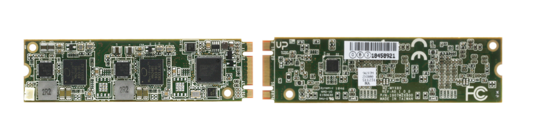
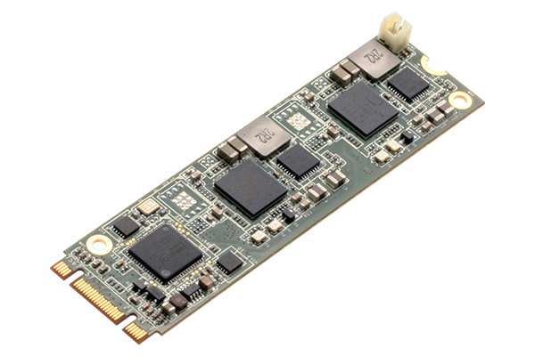
The AI Core XM2280 features two Intel Movidius Myriad X VPUs and is the first AI module from AAEON built to the m.2 standard.
AAEON, an industry leader in AI Edge computing solutions, announces the release of the AI Core XM2280, expanding the family of UP AI Core X modules powered by Intel Movidius Myriad X. The AI Core XM2280 is the first in a series of AI modules from AAEON built to the m.2 standard, and features two Myriad X VPUs.
The AI Core XM2280 is a compact solution that brings a significant upgrade in power. Equipped with two Intel Movidius Myriad X VPUs, the AI Core XM2280 is capable of up to 200 fps (160 typical) and over 2 trillion floating point operations per second as a dedicated neural network accelerator. The AI Core XM2280 is compatible with Intel’s OpenVINO tool kit and supports Tensorflow and Caffe frameworks.
The Myriad X sips energy, so the AI Core XM2280 won’t sacrifice battery life for power in your mobile applications. Its compact m.2 22×80 mm form factor allows it to fit into confined spaces. The AI Core XM2280 is perfect for bringing AI edge computing to projects such as drones, autonomous vehicles and remote camera sensors.
Features
Intel® Movidius™ Myriad™ X VPU
2x MYDX on M.2 2280 B+M key
Intel® Vision Accelerator Design SW SDK
Supported Framework: TensorFlow, Caffe, MXNET
Ubuntu 16.04, Windows® 10
AAEON is committed to providing complete AI solutions, and the AI Core XM2280 is no exception. Combined with products from our Up brand, such as the Up Extreme, the AI Core XM2280 offers a compact, flexible way to power up your project with AI edge computing. Look for more news from AAEON as we continue to expand the AI Core X and AI Core XM family with more new products planned for Q2 of 2019. Be sure to also visit Up-Board.org to learn more about how AI Core XM can power your projects.
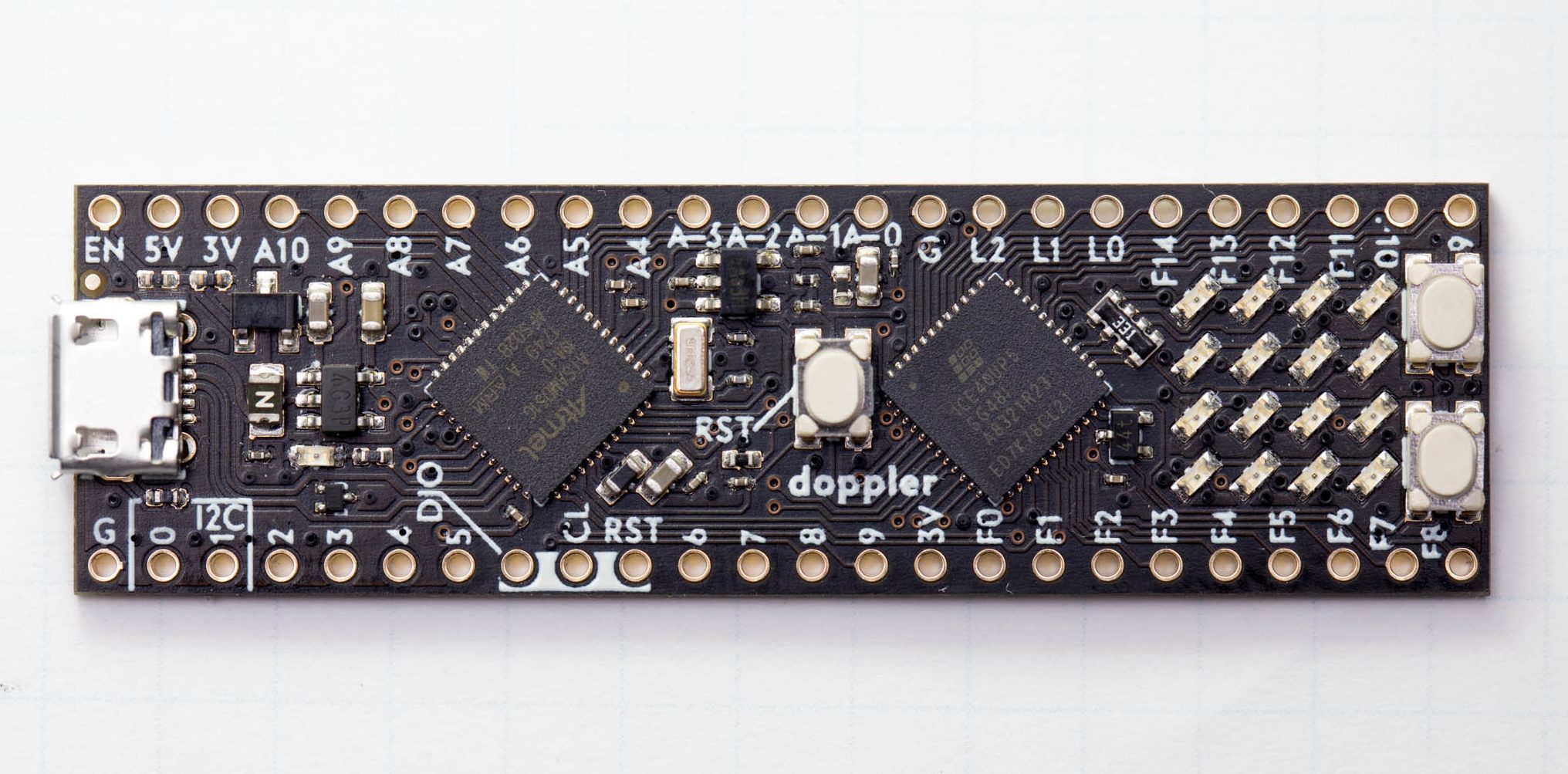
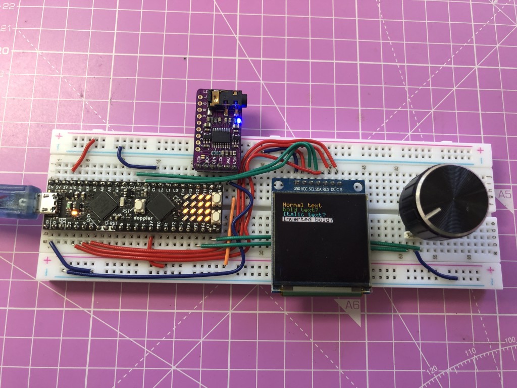
The new doppler board promises to meld the power of FPGA brains with microcontrollers and the accessibility of environments like Arduino. And the founder is so confident that could lead to new stuff, he’s making a “label” to help share your ideas.
doppler is a small, 39EUR development board packing both an ARM microcontroller and an FPGA. It could be the basis of music controllers, effects, synths – anything you can make run on those chips.
[…]
doppler takes that FPGA power, and combines it with the ease of working with environments like Arduino. It’s a chewing gum-sized board with both a familiar ARM microcontroller and an FPGA. This board is bare-bones – you just get USB – but the development tools have been set up for you, and you can slap this on a breadboard and add your own additions (MIDI, audio I/O).
doppler, on a breadboard connected to other stuff so it starts to get more musically useful. Future modules could also make this easier.
Full specs of the tiny, core starter board:
120Mhz ARM Cortex M4F MCU 512KB Flash (Microchip ATSAMD51G19A) with FPU
UF2 Bootloader with Firmware upload via simple USB stick mode
doppler is fully open source hardware, with open firmware and code samples, so it’s designed to be easy to integrate into a finished product – even one you might sell commercially.
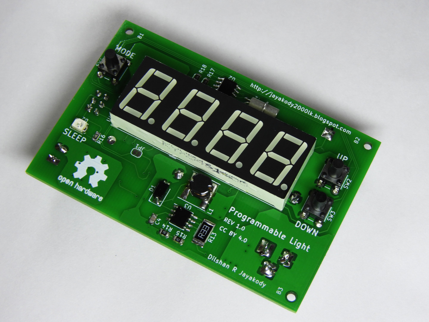
Dilshan Jayakody designed and build a programmable light controller that is able to turn ON and OFF a LED at predetermined time of each day. All the design files and source code related to this project are available at https://github.com/dilshan/programmable-light. The complete documentation of this project is also available at Github Wiki.
To meet the above requirement I designed this controller using ATmega8 MCU and DS1307 RTC. The driver stage of this light controller is intended to work with commonly available 7W LED modules. The core component of this programmable light is ATmega8 low power CMOS microcontroller. The main reason to select this microcontroller is it’s lower cost and higher availability. Except for the above two reasons this microcontroller also bundled with a rich set of peripherals which including 23 GPIOs, 3 independent timers, Two-wire serial interface, EEPROM, etc. Apart from ATmega8 microcontroller, this system uses DS1307 real time clock to maintain system time. Like ATmega8, DS1307 is also a very popular RTC in the market.
Programmable light controller with ATmega8 and DS1307 – [Link]
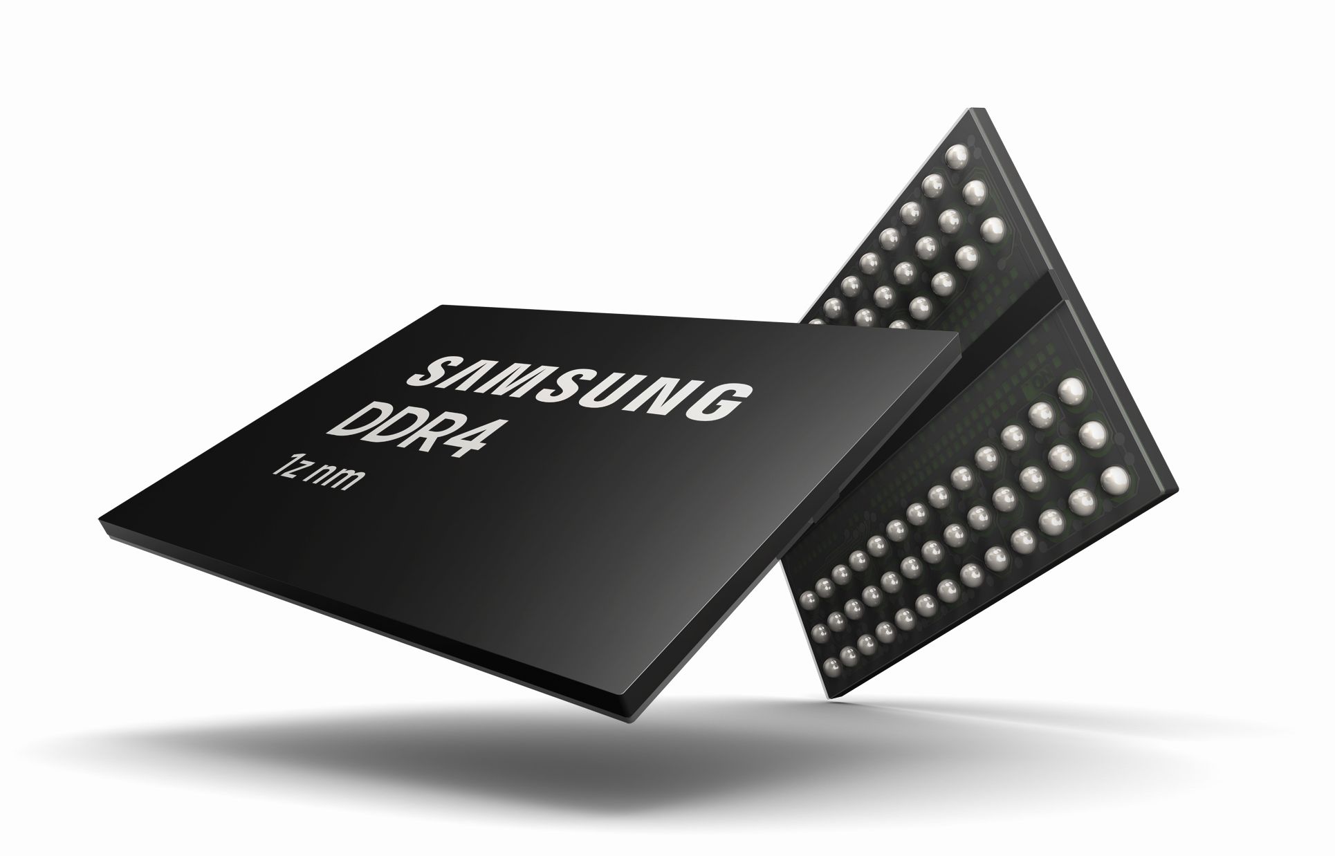
New 8Gb DDR4 based on most advanced 1z-nm process enables DRAM solutions with ultra-high performance and power efficiency.
Samsung Electronics, the world leader in advanced memory technology, today announced that it has developed a 3rd-generation 10-nanometer-class (1z-nm) eight-gigabit (Gb) Double Data Rate 4 (DDR4) DRAM for the first time in the industry. In just 16 months since it began mass producing the 2nd-generation 10nm-class (1y-nm) 8Gb DDR4, development of 1z-nm 8Gb DDR4 without the use of Extreme Ultra-Violet (EUV) processing has pushed the limits of DRAM scaling even further.
As 1z-nm becomes the industry’s smallest memory process node, Samsung is now primed to respond to increasing market demands with its new DDR4 DRAM that has more than 20-percent higher manufacturing productivity compared to the previous 1y-nm version.
Mass production of the 1z-nm 8Gb DDR4 will begin within the second half of this year to accommodate next-generation enterprise servers and high-end PCs expected to be launched in 2020.
Our commitment to break through the biggest challenges in technology has always driven us toward greater innovation. We are pleased to have laid the groundwork again for stable production of next-generation DRAM that ensures the highest performance and energy efficiency, said Jung-bae Lee, executive vice president of DRAM product & technology, Samsung Electronics.
As we build out our 1z-nm DRAM lineup, Samsung is aiming to support its global customers in their deployment of cutting-edge systems and enabling proliferation of the premium memory market.
Samsung’s development of the 1z-nm DRAM paves the way for an accelerated global IT transition to next-generation DRAM interfaces such as DDR5, LPDDR5 and GDDR6 that will power a wave of future digital innovation. Subsequent 1z-nm products with higher capacities and performance will allow Samsung to strengthen its business competitiveness and solidify its leadership in the premium DRAM market for applications that include servers, graphics and mobile devices.
Following a full validation with a CPU manufacturer for eight-gigabyte (GB) DDR4 modules, Samsung will be actively collaborating with global customers to deliver an array of upcoming memory solutions.
In line with current industry needs, Samsung plans to increase the portion of its main memory production at its Pyeongtaek site, while working with its global IT clients to meet the rising demand for state-of-the-art DRAM products.
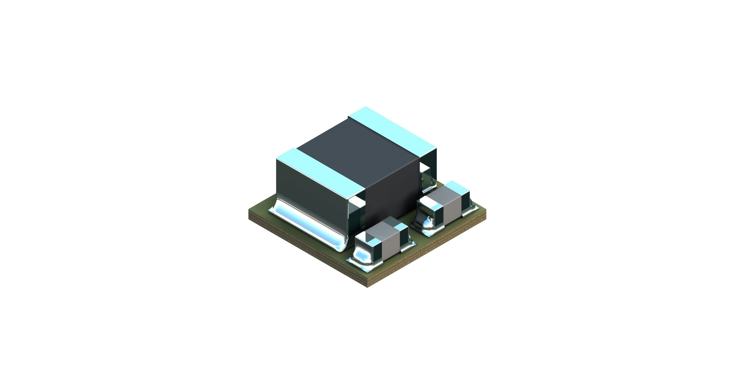
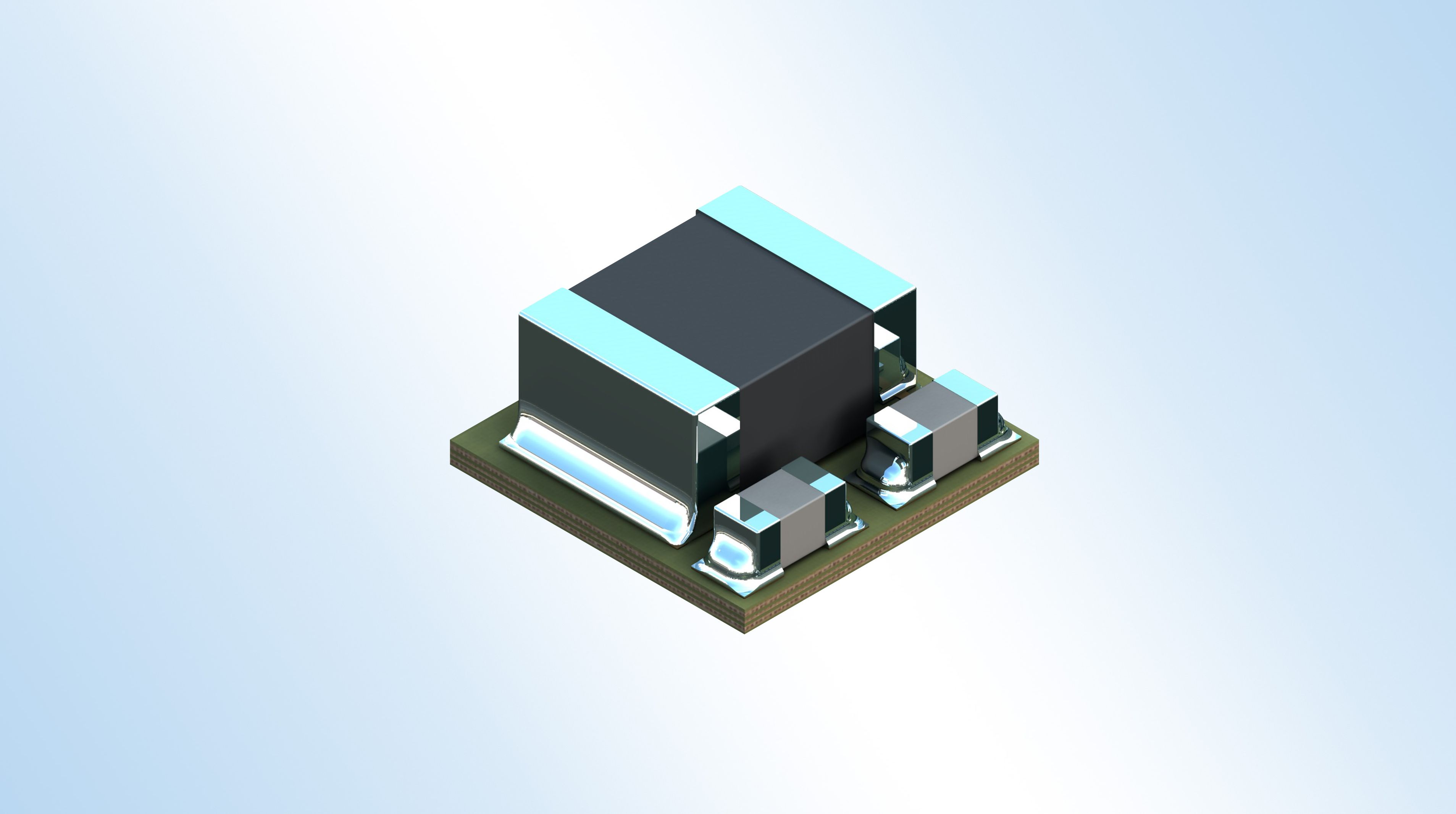
µPOL DC-DC converters bring highest power density to space-constrained apps
TDK Corporation announces the new series of µPOL™ DC-DC converters, the industry’s most compact and highest power density point-of-load solutions for applications such as big data, machine learning, artificial intelligence (AI), 5G cells, IoT and computing enterprise.
Rather than using side by side discrete integrated circuit (IC) and discrete inductor (L) the new FS series integrates the IC and inductor in a compact configuration which offers a high-density solution for space-constrained applications requiring a low-profile power source.
At 3.3 x 3.3 x 1.5 mm, they minimize the required external components, retaining the highest possible performance while offering a simplified design for ease of integration. This family can deliver a high density solution of 1 watt per mm3, while offering 50% less solution size than the other products available in its class. As a result, this minimizes system solution cost, reduces board size and assembly costs, as well as BOM and PCB costs. It operates at a broad junction temperature range, from -40 °C to 125 °C. Mass production of FS1406 is expected to begin in Q3 2019.
TDK has been developing patents related to these innovations (US 9,729,059 and US 10,193,442) over several years. µPOL™ were developed by TDK’s group company Faraday Semi. These new solutions incorporate high-performance semiconductors in advanced packaging technologies such as semiconductor embedded in substrate (SESUB) and advanced electronic components to achieve unique system integration in a smaller size and lower profile by 3D integration. This integration allows TDK to deliver higher efficiency and ease of use at a lower total system cost to what is currently available today.
μPOL™ technology includes a DC-DC converter placed in the vicinity of complex chipsets such as ASICs, FPGAs and others. By minimizing the distance between the converter and the chipset, the resistance and the inductance components are minimized, allowing fast response and accurate regulation with dynamic load currents.
The product family is rated for industrial application, is lead free and has ROHS compliance.