Banana Pi BPI-P2 Pro RK3308 IoT board offers multiple interface selection choices and reduces hardware design difficulty

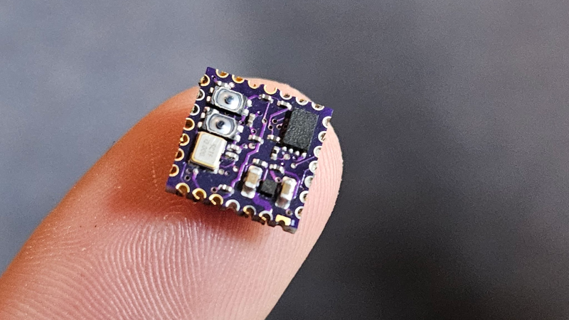
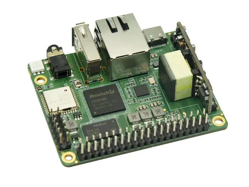
The most recent Banana Pi BPI-P2 Pro single-board computer designed for headless applications and smart audio applications, is still one to keep coming to mind when we talk about reducing hardware design difficulty and costs.

Created with an intention to meet the application needs of most embedded design engineers, the new Banana Pi BPI-P2 Pro development board comes with a rich set of interfaces such as I2S, TPM, UART, SPDIF, PCM, I2C, to mention a few. Its low power, high performance capability and Power over Ethernet support also make it an interesting board for IoT applications especially those that require a round-the-clock operation. The board can be used in any of the following smart audio application scenarios or IoT projects: industrial control, Smart Internet of Things, DIY projects, Speech Recognition, etc.

Compared to the BPI-P2 Zero and BPI-P2 Maker boards earlier released by the company, we can say that the BPI-P2 PRO is actually an upgrade as the 64-bit Rockchip RK3308 ARM chip in it is said to be faster than the Allwinner H2+ 4-core Cortex-A7 chip found in both the BPI-P2 Zero and the BPI-P2 Maker boards. The RK3308 chip also has a larger memory size of 2GB (against the 512MB) and supports a faster WIFI 5. The only downside to the BPI-P2 Pro board is that it does not come with a display interface, no GPU, and no video encoder or decoder.

Features and Specifications

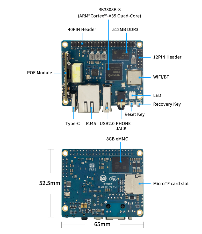
  • Newly released high-performance low-power quad-core RK3308 application SoC designed for smart AI solutions. It is characterized by multiple audio input interfaces and boasts of the following features:
    • Quad-core ARM Cortex-A35 processor at up to 1.2GHz
    • 16-bit DDR3/DDR3L/DDR2/LPDDR2
    • Embedded Hardware Voice Activation Detection (VAD)
    • ARM architecture v8-A instruction set
    • ARM Neon Advanced Single Instruction, multiple data support
    • Audio CODEC with 8x ADC and 2x DAC interfaces
    • 2x I2S/TDM, 1x multi-channel PDM interface, 1x I2S
    • High Power efficiency
    • Designed for accelerated media and signal processing applications such as intelligent voice interaction, smart audio I/O processing etc.
  • Up to 2GB DDR2 SDRAM memory
  • 8GB eMMC onboard
  • Micro SD card slot
  • Headphone jack
  • Dual-band WiFi (AP6256) and Bluetooth onboard
  • 1x USB 2.0, 1x USB Type-C
  • 40x pin GPIO expansion header and 12x pin GPIO header
  • Power and Status LED, reset button and recovery key (1x each)
  • Type-C 5V/2A or PoE (36V – 57V input)
  • Weight: 30 grams
  • Dimension: 65.0 mm x 52.5 mm
  • Operating System: Linux, Debian or Ubuntu OS

The headless Banana Pi BPI-Pro headless SBC with PoE module is currently selling on AliExpress for around $31 including shipping. Further details on the board can also be found there.

ICP Introduces DRPC-124-EHL, an Ultra-Compact PC with Intel Celeron J6412 CPU and 2.5 GbE LAN

The DRPC-124-EHL by ICP Germany is an ultra-compact, DIN-rail, Fanless Mini PC with a 10nm Intel Celeron Quad Core J6412 processor and four LAN ports.

The DRPC-124-EHL by ICP Germany is an ultra-compact, DIN-rail, Fanless Mini PC with a 10nm Intel Celeron Quad Core J6412 processor and four LAN ports.

The DRPC-124-EHL is a compact DIN-rail mini PC powered by an Intel Celeron J6412 processor. The nominal clock speed of the device is 2.0 GHz, which can boost up to 2.6 GHz with a max TDP of 10W. Besides that, this mini PC comes with a dual 2.5GbE Ethernet and is equipped with 8GB of LPDDR4x memory, expandable up to 16GB. In terms of storage, the device comes with 64GB or 128GB storage options. The device uses a 2-pin terminal block with a 12-28V DC input for power.

The DRPC-124-EHL by ICP Germany is an ultra-compact, DIN-rail, Fanless Mini PC with a 10nm Intel Celeron Quad Core J6412 processor and four LAN ports.

The IntelCeleron-J6412 is a 4-core, 4-thread processor with a maximum boost frequency of 3.6GHz and a 1.5 MB L2 Cache. Other than that, it has 16 Execution Units and support for Intels 11th Gen UHD Graphics; with all the features, the total TDP of this device is only 10 Watts, which is very impressive for a device like this.

Regarding Ethernet Connectivity, this device offers Four Intel Ethernet ports, among those there is one GbE interface with an I210 controller and three 2.5 GbE interfaces with an I225V controller. The device comes with Windows 10 preinstalled but it is also compatible with Linux. other than that, when it comes to certifications its CE, FCC, and UKCA certified.

Specification of DRPC-124-EHL Module

  • Memory/Storage: Up to 16GB LPDDR4x, Up to eMMC 5.1 128GB.
  • Display: 1x HDMI V 1.4B.
  • Expansion: 1x 2242 B-key (PCIe Gen3 x2), 1x 2242 B-key (SATA), 1x 2280 M-key (PCIe Gen3 x2).
  • Connectivity: 1 x RJ-45 PCIe GbE, 3 x RJ-45 PCIe 2.5.
  • I/O Interfaces: 1x RS-232/422/485 (Optional).
  • USB: 2 x USB 3.2 Gen2, 2 x USB 2.0.
  • Other Features: TPM 2.0.
  • Power: 12-28 VDC (via 2-pin terminal block).
  • Operating Temperature: 10°C to 50°C.
  • Mechanical: 159 x 132.5 x 35 mm, 1.2 kg, DIN-Rail, Wall Mount, extruded aluminum alloy chassis.

ICP did not disclose any pricing information about the DRPC-124-EH mini PC at the time of writing this article. The device can be found on the official product page of ICP.

World’s Smallest RP2040 Development Board RPDot

rp2040-small-board

With a net dimension of 10x10mm, William Herr’s RPDot board makes headlines as the smallest RP2040 board in the market. 

When it comes to dimensions the RP2040 IC only measures 7x7mm, while the overall dimensions of the board extend to 10x10mm. According to a recent hackday post by William Herr “I got the idea from Solder Party’s RP2040 Stamp, but I thought that it could be designed smaller.” In that post, he also said, “I settled on 10×10mm because of the ability to route traces around the RP2040 and have some room for castellated edges.”

smallest-rp2040-board-with-0201-parts

Resistor capacitors and voltage regulators are the most significant components in any electronic design so choosing them was an issue. Still, before designing the board, it was inevitable that with 0201-sized parts, this board would be possible to build. But the biggest hardel in the circuit was the voltage regulator, so in his article, he had to choose a 3.3V 300mA regulator with a footprint of (1mmx1mm).

At the start of the design process, it was evident that the board would be at least a 4-layer board, but, in hindsight, it would have been much better as a 6-layer board. But the price of a 6-layer board was much too high for a single prototype. So a four-layer board it was. But to make the board work he had to break certain design conventions. to compensate for the reduced layer count he had to add a few traces into the GND plane.

Another challenge for the board design was to choose which pins go on to the castillated edges. After careful consideration, the SWD, all power lines, USB, and all ADC pins are chosen to go onto the edge. Other than that there are also some digital pins that are close to the edge.

The result is a tiny, hand-assembled, surface-mountable stamp module, making the RP2040 Stamp seem huge in comparison. It was assembled using a stencil, ancient lead-free solder paste, a hot plate, a 3D-printed jig, and a hot-air station.  More details and updates can be found on the engineer’s Hackaday.io page.

BeagleV-Ahead: RISC-V Raspberry Pi Replacement?

In the SBC industry, long dominated by devices like Raspberry Pi and their competitors, BeagleBoards aims to bring innovation by announcing their new BeagleV-Ahead SBC based on the new RISC-V architecture.

RISC-V is an Instruction Set Architecture (ISA) released in 2015 that has proven to be compatible with a wide variety of hardware concerning power, performance, size, and complexity. Historically, SBCs like Raspberry Pis used ARM SoCs to achieve their performance target on small form factor boards. This introduced a limiting factor in compatibility with the board’s choice of software and the performance these processors provided. Despite these limitations, the ARM processors were enough for many IoT-related applications and were widely adopted for their platform support.

What makes the BeagleV-Ahead different?

BeagleBoards, the manufacturer of the BeagleV-Ahead, has designed it to be versatile, powerful, and a compelling option against the mainline SBCs. Thus, the BeagleV-Ahead shares many similarities with a Raspberry Pi 4 in features but is also different in its functionality.

Powering this board is an Alibaba T-Head TH1520 RISC-V SoC with 50 GFLOPS BXM-4-64 GPU, 4 GB LPDDR4 RAM with 16 GB of eMMC storage. It is also equipped with a 4 TOPS INT8 NPU and 2 ISPs which are helpful for image recognition and other machine-learning tasks without requiring additional equipment. Besides all the necessary GPIO found on mainline SBCs like UART, PWM, and I2C, the board is also kitted out with 2 USB connections, Ethernet as well and Micro HDMI. Also, wireless connectivity is provided via the latest standards of WiFi and Bluetooth.

BeagleV Vs Raspberry PI

The Capes Ecosystem of Shields

For adding functionality to the board, BeagleBoards has an alternative like the Raspberry Shields. BeagleBoards markets ‘Capes’ as add-on shields that are specifically designed for boards in the BeagleBone and PocketBeagle family to add more functionality to the existing package without much hassle. MikroBus pin-outs in combination with Capes, can provide an advantage in the development of applications with requirements of large amounts of I/O in less amount of time.

BeagleV-Ahead Features

Linux Powers the RISC-V Board

The BeagleV-Ahead supports Android, FreeRTOS, Fedora, and Linux (even mainline Linux) as the official operating systems. This ensures that the software remains open-standard, developer-friendly, and widely accessible for the development of new projects for the RISC-V architecture.

While the AI and machine-learning capabilities of this board are complemented by Linux, the speed of the NPU and the non-configurable 4GB of RAM limit the applications to the likes of running pre-trained data models or certain calculation accelerations.

RISC-V, being a somewhat new architecture implies that immediate support for all the hardware features as well as pre-developed applications is a rare occurrence and support might flourish once the new architecture gains a wider user base. For developers and users looking for immediate solutions, they should consider other options on the market not based on RISC-V or develop the applications themselves.

Conclusion

In conclusion, the BeagleV-Ahead is a great SBC alternative to the Raspberry Pi with all its features and also the RISC-V architecture. This board also provides a good testing ground for developers who are looking into the development of applications based on the RISC-V architecture.

The Beagle-V Ahead is distributed by various channels and more information can be found on their official webpage. For more information, refer to the documentation.

High-Performance Mixtile Core 3588E: A Compact System-on-Module with Advanced AI Capabilities

Mixtile Core 588E SOM by Mixtile: A high-performance System on Module powered by Rockchip RK3588 SoC, designed for compatibility with NVIDIA Jetson TX2 NX carrier boards.

Mixtile develops Core 588E SOM, a high-performance SOM with an edge connector. Powered by Rockchip RK3588 SoC, this board is compatible with NVIDIA Jetson TX2 NX carrier boards.

Mixtile, a well-known IoT hardware and compute module manufacturer, has recently announced the mixtile core 3588E System on Module. The SOM boasts a powerful Rockchip RK3588 SoC with a 260-pin SO-DIMM connector. The system designers at Mixtile designed the board to be compatible with NVIDIA Jetson TX2 NX carrier boards, making the integration process seamless.

The Rockchip RK3588 system-on-chip ships with four Arm Cortex-A76 high-performance cores at 2.4GHz and four Cortex-A55 low-powred cores at 1.8GHz. It also has a Mali-G610 graphics processor with 6 TOPS NPUs. There’s also 15GB eMMC storage as standard and support for an 8K video encoder and decoder. Designed with the latest 7nm Technology, the total TDP of this device is only 7W. The company has confirmed that the module includes four PCI Express Gen 3 lanes for external accelerators or other hardware integration.

Mixtile Core 3588E: Compute Module Specifications

  • SOC is A Rockchip RK3588.
  • Features an octa-core CPU with 4x Arm Cortex-A76 (2.4 GHz) and 4x Arm Cortex-A55 (1.8 GHz).
  • GPU is the Arm Mali-G610 MP4, supporting various graphic standards.
  • VPU supports multiple video formats, including 8K, and encodes 8K H.265/H.264 and JPEG.
  • NPU is 6 TOPS for generic AI tasks.
  • It comes with 8GB, 16GB, or 32GB LPDDR4 Memory configurations.
  • Internal storage is 32GB eMMC 5.1 flash.
  • It uses a standard 260-pin SO-DIMM, compatible with Jetson designs.
  • It has support for the SD 3.0 interface.
  • Has Support for HDMI 2.1 (up to 8Kp60), DisplayPort 1.4, and MIPI DSI.
  • Offers multiple MIPI CSI connections for cameras.
  • Audio can be accessed by interfacing with the 2x I2S ports.
  • supports a Gigabit Ethernet connection.
  • USB Port Includes 2x USB 3.0 and 2x USB 2.0 ports.
  • PCIe Features include a PCIe Gen 3.0 slot.
  • It requires 5V @ 3A via a USB-C port.
  • It measures 69.6 x 45 mm in size.
  • Operating Temperature is -20°C to 70°C and can be stored between -40°C to 85°C.

Mixtile provides Android 11 and Debian 11 BSPs for the Rockchip RK3588 module. On the other hand, the Jeston Nano module comes with Ubuntu 18.04 or 20.04. Apart from the software difference, the Mixtile’s module is expected to give more value for its cost compared to the NVIDIA Jetson modules. However, that depends on the use case.

According to the product page, the Mixtile core 3588E SOM is available to order in two variants — the 4GB model comes at $109, and the 16GB version at $159; they also announced a 32GB version, but it is not available at the time of writing this article.

The pricing is based on an early bird pre-order, which is already 18% less than the original price. But they will increase on August 31. Additionally, these devices are expected to be delivered in mid-October via international air mail.

Why Mixtile Core 3588E?

  • Powered by Rockchip RK3588 SoC with a 260-pin-SO-DIMM connector compatible with NVIDIA Jetson TX2 NX
  • 6 TOPs AI performance supports Large Language Models (LLMs) such as GPT, LLaMA, ChatGLM, and Bloom
  • Support creating an ARM Server with clusters of up to 75 Core 3588E SoMs in a standard 2U, 19-inch chassis
  • Industrial-grade Mixtile Core 3588JE can withstand temperatures from -40 °C to 85°C for extended periods

UPDATE: 2/2/2024: The Mixtile Core 3588E is in stock and shipping now for $109.00 – $278.00 depending on configuration.

Starting on February 7, Mixtile Core 3588E SoM will officially resume its original price as follows:

  • $109 -> $132 (4GB RAM+32GB eMMC)
  • $159 -> $190 (16GB RAM+128GB eMMC)
  • $269 -> $329 (32GB RAM+256GB eMMC)

JLCPCB Revolutionizes Metal 3D Printing with a Remarkable 40% Price Reduction

JLCPCB, a pioneering force in PCB prototyping, has announced a remarkable up to 40% price reduction in its metal 3D printing services, a strategic move that underscores their commitment to accessible innovation. This reduction in costs opens new doors for industries to leverage the potential of metal 3D printing, from aerospace to healthcare. JLCPCB’s dedication to maintaining quality while making advancements affordable cements its reputation as an industry leader. This milestone stands as an invitation for both existing and new customers to explore the possibilities of metal 3D printing, further propelling JLCPCB’s journey of technological excellence.

JLCPCB, a pioneering name in PCB and SMT prototyping, has once again taken the lead in innovation by announcing an astonishing up to 40% price reduction in its metal 3D printing services. This strategic move comes as a result of the company’s continuous commitment to providing cutting-edge solutions that are not only high in quality but also affordable for a wide range of customers.

In 2022, JLCPCB entered the 3D printing arena, extending its expertise from PCBs and SMT to offer 3D printing services. Recognizing the considerable expense associated with metal printing, the company embarked on a mission to diversify options for its customers. This endeavor aligned seamlessly with JLCPCB’s legacy of delivering value-driven solutions to its clients.

The focal point of this major price reduction lies in JLCPCB’s concerted efforts to curtail production costs. One notable achievement is the company’s substantial expansion of its metal printing manufacturing capacity, which has been increased by an impressive fivefold. By optimizing material utilization and employing advanced production technologies, JLCPCB’s R&D teams have significantly reduced overall costs.

“JLCPCB SLM 3D printing service is so speedy and easy-to-use. Now we can use metal 3D printing not only for making parts for business, but also for hobby because they also offer an affordable price. It’s a game changer!,” stated Ryota Suzuki, the founder of TYE’s Tech Lab. “Our decision to substantially reduce the cost of metal 3D printing underscores our dedication to making advanced manufacturing processes accessible to a broader spectrum of industries. This milestone not only benefits our existing clients but also extends a warm invitation to new customers who can now explore the advantages of metal 3D printing without the inhibitions of high costs.”

This strategic move is bound to disrupt the metal 3D printing landscape. With reduced costs, manufacturers and designers can now harness the potential of metal 3D printing for various applications, including aerospace, automotive, healthcare, and beyond. The cost-effectiveness of JLCPCB’s services opens doors to rapid prototyping and low-volume production without compromising on the quality and precision the metal 3D printing is renowned.

Video

As JLCPCB takes this leap, it remains steadfast in its commitment to maintaining the high quality and precision that customers have come to expect. The company’s reputation as an industry leader is built upon a foundation of trust, reliability, and technological excellence.

In conclusion, JLCPCB’s groundbreaking up to 40% price reduction in metal 3D printing services, coupled with its expansion of metal printing manufacturing capacity, stands as a testament to its unwavering dedication to innovation and customer satisfaction. By mitigating cost barriers and expanding the horizons of metal 3D printing, JLCPCB is poised to empower industries and individuals alike to bring their boldest ideas to life.

For further information, and inquiries, and to explore the world of affordable metal 3D printing, please visit JLCPCB Online 3D Printing Service.

cover photo: depositphotos.com

New Rugged i.MX8M Plus 6x GbE Single Board Computer

Gateworks is proud to announce the release of the Venice GW7400 Industrial Single Board Computer. This is the most powerful member of the Venice family and based on the NXP i.MX8M Plus 64-Bit Quad Core ARMv8 SoC. The processor features a Neural Processing Unit (NPU), VPU, GPU and DSP. This rugged SBC features six Gigabit Ethernet ports, three Mini-PCIe slots for WiFi and one M.2 slot with dual SIMs for cellular modems. The GW7400 additionally features USB 3.0, dual CAN Bus, DIO, I2C, SPI and UART interfaces. A TPM 2.0 secure crypto-processor is optional for ensuring system security and integrity. The Gateworks System Controller (GSC) provides advanced system health monitoring, RTC, secure key storage and power control.

Gateworks Venice GW7400 Highlights:

  • NXP i.MX8M Plus Quad Core CPU at 1.6GHz
  • 1GB LPDDR4 RAM (4GB Optional)
  • 8GB eMMC Flash (64GB Optional)
  • Six GbE Ports for wired connectivity
  • Three Mini-PCIe Sockets for WiFi or Cellular
  • M.2 Slot with Dual SIM for 5G Cellular Modems
  • USB 3.0, DIO, SPI, I2C, UART, ADC Interfaces
  • Dual CAN Bus
  • Digital 3-axis MEMS Accelerometer
  • Optional TPM, GPS, WiFi/BLE
  • Industrial Temperature -40 to +85C
  • Ubuntu Linux BSP
  • Made in USA

The GW7400 is available now in both standard and max versions. The max version features 4GB DRAM memory and 64GB eMMC Flash memory along with TPM, GPS and WiFi/BLE loaded.

The rugged and powerful GW7400 excels in handling any gateway or networking application.

Low-Power IB838 Single Board Computer Powered by Intel Core i3 N-series (Alder Lake-N) Processor

IBASE Technology Inc., a renowned provider in the design and manufacturing of embedded computing solutions, rolls out the low-power IB838 3.5” single board computer powered by Intel® Core™ i3 N-series (formerly Alder Lake-N) processor. Combining robust computing performance with advanced features, it is positioned to meet diverse needs across multiple industries, including industrial automation and control, retail displays, transportation, and automotive applications.

Fortified with intelligent power handling and a 9V~36V DC input range, the IB838 ensures reliability and consistent operations in transportation applications that may encounter variable power conditions. Versatile connectivity makes it ideal for automation processes and data acquisition systems. The SBC offers Type-C, DP++, and eDP or LVDS display options, along with a rich set of I/O interfaces, including two Intel® PCI-E 2.5G LAN ports, two USB 2.0 ports, and four USB 3.2 ports (1x Type-C + 3x Type-A).

IB838 FEATURES:

  • Intel® Core™ i3 N-series (formerly Alder Lake-N) processor
  • 1x DDR5 SO-DIMM, Max. 16GB
  • Supports Type-C & DP++ and eDP or LVDS
  • 2x Intel® PCI-E 2.5G LAN
  • 2x USB 2.0, 4x USB 3.2 (1x Type-C + 3x Type-A), 4x COM, 1x SATA III
  • 2x M.2 sockets (E-key + B-key), supports CNVi
  • 9V~36V wide-range DC input
  • Supports fTPM, Watchdog timer, Digital I/O

With CNVi support, the 5G-ready IB838 comes equipped with a high-speed SATA III port and two M.2 sockets (E-key + B-key), providing ample storage and expansion possibilities. Additionally, it boasts four serial ports and digital I/O, facilitating comprehensive connectivity to diverse devices and peripherals. Enhanced security and functionality are integrated through fTPM (firmware-based Trusted Platform Module) and a Watchdog timer for system stability. For more information, please visit www.ibase.com.tw

New 4X4 BOX 7040 Series Mini PC: Sprint Faster and Run Longer with AMD Ryzen™ 7040U Series APU

ASRock Industrial releases the 4X4 BOX 7040 Series Mini PCs powered by AMD Ryzen™ 7040U Series APUs, featuring up to 8 “Zen 4” cores and 16 threads. With the new AMD Ryzen™ AI, the first AI engine for an x86 platform, and support of dual-channel DDR5 5600MHz memory up to 64GB, the new Series sprint ahead in speed, performance, and AI capability, while guaranteeing extended runtime. The 4X4 BOX 7040 Series comes with enriched I/O connectivity in a compact appearance, enabling 4K quad-display outputs, five USB ports with two USB4, dual storages, and dual LAN up to 2.5G, Wi-Fi 6E. The faster performance with AI engine and longer runtime bring about productivity boost and next-level experience in content creation, gaming, entertainment, commerce, and many other AIoT applications.

AMD Ryzen™ 7040U Series APU with DDR5 5600 RAM

Powered by AMD Ryzen™ 7040U Series APU (Ryzen™ 7 7840U/Ryzen™ 5 7640U), ASRock Industrial’s 4X4 BOX 7040 Series contain selections: 4X4 BOX-7840U and 4X4 BOX-7640U. Featuring 4nm “Zen 4” architecture with up to 8 cores and 16 threads, and enhanced dual-channel DDR5 5600MHz SO-DIMM memory up to 64GB, the Series guarantee faster productivity, content creation, and gaming with extended runtime. Moreover, with built-in AMD Ryzen™ AI – the pioneer of dedicated AI hardware in an X86 processor, the 4X4 BOX 7040 Series usher in advanced potentials in power, efficiency, and intuition for the future AI working world. This integration transforms the 4X4 BOX 7040 Series into a reliable personal virtual assistant, propelling dynamic AI applications, enhancing video conferencing, and delivering AI-inspired visuals.

Rich I/O Connectivity in Compact Appearance

The 4X4 BOX 7040 Series’ enriched I/O connectivity in a compact size of 117.5 x 110 x 47.85 mm comes with two USB4, one USB 3.2 Gen2 (Type-A), and two USB 2.0 ports, one audio jack, one DC jack. With integrated AMD Radeon™ Graphics, the Series support 4K quad-display outputs through two HDMI 1.4b and two DisplayPort 1.4a (two from Type-C), providing outstanding visual experience upgrades. For dual-storage, the Series include one SATA3.0 and one M.2 (Key M, 2242/2260/2280) with PCIe Gen 4×4 for SSD for maximum scalability. Besides, the 4X4 BOX 7040 Series are equipped with dual LAN ports- one 2.5G and one 1G port with DASH for remote management, alongside Wi-Fi 6E and Bluetooth 5.2 support to deliver high-speed communication. The 4X4 BOX 7040 Series sprint in the lead with versatile connectivity, perfect for multi-faceted usages.

Here’s more: 4X4 7040 Motherboard Series

ASRock Industrial also introduces 4X4 7040 Motherboard Series powered by AMD Ryzen™ 7040U Series APU (Ryzen™ 7 7840U/Ryzen™ 5 7640U), inclusive of 4X4-7840U and 4X4-7640U. Key features comprise two SO-DIMM DDR5 5600 MHz up to 64GB memory support, dual LAN up to 2.5G, and 4K quad-display through two HDMI 1.4b and two DP 1.4a (with two from Type-C). Optimized overall capacity are achieved by I/O connectivity and expansions with two USB4, two USB 3.2 Gen2, two USB 2.0, one M.2 Key E slot, and dual storage supported by one M.2 Key M and one SATA3.0. Moreover, a 12~19V DC-in design with flexible power input, 0~70°C wide range operating temperature, while AMD FW TPM is for software-based security. The 4X4 7040 Motherboard Series can bring about next-level business and embedded solutions, plus enhanced gaming experience and productivity boost on PCs.

Sprint Faster, Run Longer – the 4X4 BOX 7040 Series and 4X4 7040 Motherboard Series powered by AMD Ryzen™ 7040U Series APU, have arrived to unlock unprecedented possibilities in computing speed, graphics performance, and runtime. With significant enhancement of CPU, GPU, and extended runtime, this compact Mini PC and Motherboard Series are ready to sprint ahead in applications across diverse fields.

For more detailed product information, please visit our Website or contact us at Product Inquiry.

e-peas Introduces First Energy Harvesting PMIC to Handle Two Independent Energy Sources at the Same Time

AEM13920 gives valuable new flexibility to deploy the ideal mix of PV, RF, thermal and kinetic energy sources for the application

e-peas, the leading supplier of energy harvesting ICs, today launched its first PMIC that can handle simultaneous inputs from two independent harvested energy sources.

The new AEM13920 can maximize the energy harvested from any combination of two sources, including photovoltaic (PV) cells, a thermo-electric generator (TEG), RF energy harvester, or pulsed (kinetic) energy sources. Before the introduction of the AEM13920, specialized PMICs have been optimized for a single type of energy harvester.

The flexible dual-source capability opens up interesting new design options for the use of energy harvesting in small electronic devices such as remote controls, PC peripherals, wireless sensors and more. For instance, a remote control could have separate PV cells on its front and rear, to maintain an energy input whether the device is left face up or face down. A smart wireless light switch could operate on mechanical energy for short RF transmissions, and on stored mechanical or light energy for longer operations such as downloading and installing a firmware update.

In these and other applications, the AEM13920 provides a complete power management solution that maximizes energy recovery from the source. In the AEM13920, e-peas has also added valuable new features for system optimization and protection.

The PMIC achieves ultra-high source-to-storage and storage-to-load conversion efficiencies of higher than 90%. Independent maximum power point tracking (MPPT) algorithms for each source, and an ultra-low cold-start input condition of 275 mV/5 µW, maximize the amount of energy drawn from any type of harvester. The AEM13920 also offers the option of constant source-voltage regulation.

Use of the AEM13920 simplifies power-system development and minimizes component count and bill-of-materials cost, because it implements in a single chip all the functions required to store and use energy from an external harvester. Two independent on-chip boost converters manage source voltage conversion and the supply to the storage element. A separate on-chip buck regulator converts the output from the storage element to a fixed voltage required by the application between 0.6 V and 2.5 V. The AEM13920 also manages a 5 V power input, which can be used to charge the storage element in the event of a prolonged period of operation without an input from an energy harvester.

New control and configuration features introduced in the AEM13920 include:

  • Average Power Monitoring – a circuit which measures total energy transferred from each of the two sources to storage, and total energy supplied to the load. This enables the host microcontroller to calculate the state of charge of the storage element, and to monitor system operation in detail.
  • I2C interface for control of 33 register settings by the host MCU, and for system data read-outs

The AEM13920 also offers a full suite of system monitoring and protection features, including:

  • Thermal monitoring of the storage element
  • Selectable over-charge and over-discharge limits for protection of the storage element
  • Shipping mode to protect the storage element

The AEM13920 is compatible with many types of rechargeable batteries and storage elements, including lithium-polymer, LiFP and li-ceramic batteries, and hybrid lithium capacitors.

Christian Ferrier, Chief Marketing Officer of e-peas, said: ‘e-peas has been pioneering the technology of energy harvesting for years, and the AEM13920 is the latest product of our innovation – a fully integrated PMIC that enables designers to use the combination of two energy sources that is exactly right for their application.

‘And because our technology is so efficient and effective, the AEM13920 should encourage more OEMs to stop relying on wasteful primary batteries, and so reduce the amount of electrical waste that goes to landfill.’

The AEM13920 is supplied in a 40-pin QFN package with a board footprint of 5mm x 5mm. It is available for sampling now. For sample requests and for information about the 2AAEM13920J051 evaluation board, go to www.e-peas.com.

TOP PCB Companies