New PicoScope 9400 5 GHz oscilloscope

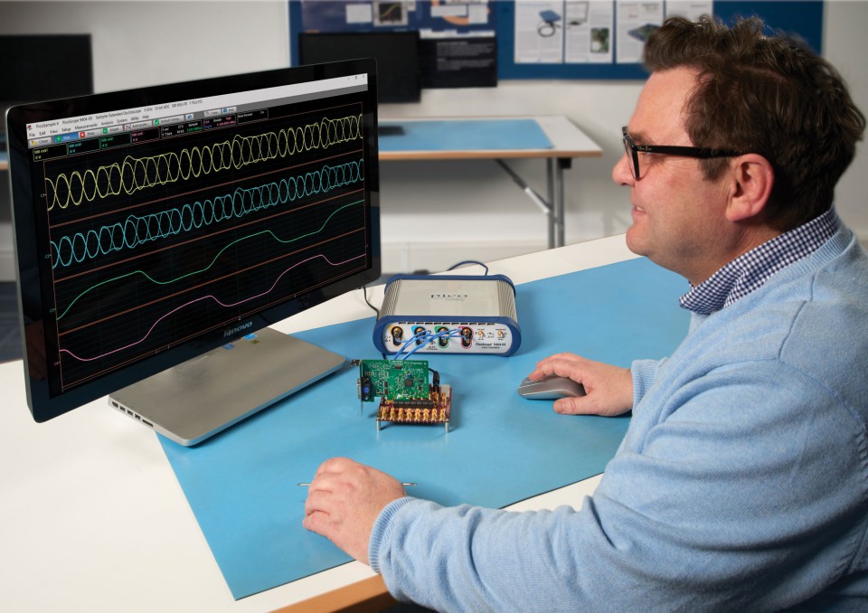
The PicoScope 9404-05 is the first of a new class of oscilloscopes that combine the benefits of real-time sampling, equivalent-time sampling and high analog bandwidth.

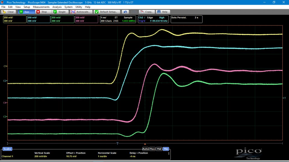
The PicoScope 9404-05 has four 5 GHz input channels with market-leading ADC, timing and display resolutions for accurately measuring and visualizing high-speed analog and data signals. It is ideal for capturing pulse and step transitions to 70 ps, impulses down to 140 ps and clocks and data eyes to 3 Gb/s. Most high-bandwidth applications involve repetitive signals or clock-related data streams that can be readily analyzed by equivalent-time sampling (ETS). The SXRTO is fast: it quickly builds ETS, persistence displays and statistics with up to 2 million triggered captures per second. The PicoScope 9404-05 has a built-in full-bandwidth trigger on every channel, with pretrigger ETS capture to well above the Nyquist sampling rate. There are three acquisition modes—real time, ETS and roll—all capturing at 12-bit resolution into a shared memory of 250 kS.

Features

  • 5 GHz bandwidth, 70 ps transition time
  • 1 TS/s (1 ps) equivalent-time sampling
  • Four 12-bit 500 MS/s ADCs
  • Pulse, eye and mask testing to 70 ps and 3 Gb/s
  • Up to 2 million triggered captures per second
  • Logical, configurable, touch-compatible Windows user interface
  • Comprehensive built-in measurements, zooms, data masks and histograms

The PicoSample 4 software is derived from our existing PicoSample 3 and PicoScope 9000 products, which together represent over ten years of development, customer feedback and optimization.

The high-resolution display can be resized to fit any window, filling 4k and even larger monitors or arrays of monitors. Four independent zoom channels can show you different views of your data down to a resolution of 1 ps. Most of the controls and status panels can be shown or hidden according to your application, allowing you to make optimal use of the display area.

The oscilloscope has a 2.5 GHz direct trigger that can be driven from any input channel, and a built-in prescaler can extend the trigger bandwidth to 5 GHz.

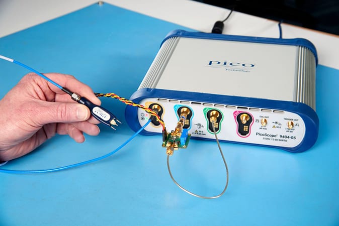
These compact units are small enough to place on your workbench close to the device under test. Now, instead of using remote probe heads attached to a large benchtop unit, all you need is a short, low-loss coaxial cable. Everything else you need is built into the oscilloscope, with no expensive hardware or software add-ons to worry about, and we don’t charge you for new software features and updates.

Typical applications

  • Telecom and radar test, service and manufacturing
  • Optical fiber, transceiver and laser testing (optical to electrical conversion not included)
  • RF, microwave and gigabit digital system measurements
  • Signal, eye, pulse and impulse characterization
  • Precision timing and phase analysis
  • Digital system design and characterization
  • Eye diagram, mask and limits test to 3 Gb/s
  • Ethernet, HDMI 1, PCI, SATA, USB 2.0
  • Semiconductor characterization
  • Signal, data and pulse/impulse integrity and pre-compliance testing

High-bandwidth probes

The PicoConnect 900 Series low-impedance, high-bandwidth probes are ideal companions for the PicoScope 9404-05, allowing cost-effective fingertip browsing of fast signals. Two series are available:

Overview Video

Other features

Bandwidth limit filters

A selectable analog bandwidth limiter (100 or 500 MHz) on each input channel can be used to reject high frequencies and associated noise. The narrow setting can be used as an anti-alias filter.

Frequency counter

A dedicated frequency counter shows signal frequency (or period) at all times, regardless of measurement and timebase settings, with a resolution of 1 ppm.

Three quantum computer components integrated on one chip

Scientists at the University of Stuttgart and the KIT succeed in important further development on the way to quantum computers.

Quantum computers one day should be able to solve certain computing problems much faster than a classical computer. One of the most promising approaches is based on the utilization of single photons to carry and process quantum information. Scientists of the University of Stuttgart and the Karlsruhe Institute of Technology (KIT) were now able to integrate three necessary main components (single-photon source, beamsplitters and single-photon detectors) on a single chip and operate it on the single-photon level. This experiment demonstrates the functionality of the basic components for a scalable system for photon-based quantum information processes.  The results got published in Nano Letters.


Photonic circuit in which single photons are emitted, guided and split into two waveguide-arms. The detection is done on-chip via integrated detectors at the end of the two waveguides arms, the reflecting metal layers help to suppress stray light coming from the excitation laser.
Photo: University of Stuttgart/Mario Schwartz

In contrast to the widespread silicon technology, the experiment was implemented on a gallium arsenide (GaAs) platform, allowing the direct integration of nanometer-sized structures, called quantum dots (QDs), which can serve as efficient on-demand sources of single photons. In addition, GaAs allows guiding these single photons to optical logic circuits and to special on-chip detectors made of superconducting nanowires. In the experiment, single photons emitted by an optically pumped quantum dot were guided inside a photonic waveguide and divided by an on-chip beamsplitter into two waveguide-arms, each equipped with a detector.

“One of the challenges so far in this type of fully on-chip experiment was the close proximity of the excitation laser to the on-chip detectors”, explains Mario Schwartz.

The PhD student from the Institute of Semiconductor Optics and Functional Interfaces (IHFG), University of Stuttgart, was working over the last years on the realization of a proof-of-principle experiment to show the feasibility of combining all main components on one single photonic chip. The project was realized in close collaboration with the PhD student Ekkehart Schmidt from the KIT, who is an expert for the design and implementation of the on-chip detectors.

“The detectors cannot distinguish photons coming from the laser and photons coming from the quantum dot, leading to undesirable detection events”, Schmidt further points out.

The scientists were able to significantly reduce the influence of the laser photons by implementing reflecting metal layers on the chip. This idea allowed the verification of the quantum nature of the QD emission by using only the on-chip components. “The successful experiment is an important step forward and demonstrates the potential of fully integrated photonic circuits with all main components being implemented on a single chip.

We foresee clear possibilities of increasing the device complexity in the near future” says Prof. Dr. Peter Michler, director of the IHFG, University of Stuttgart.

Prof. Dr. Peter Michler, Mario Schwartz, Florian Hornung, University of Stuttgart, Institute of Semiconductor Optics and Functional Interfaces (IHFG) [via]

Nitrogen8M Mini is the First SBC with i.MX8M Mini SoC

Boundary Devices has unveiled its “Nitrogen8M-Mini” SBC, the first SBC that is based on NXP’s new i.MX8M Mini SoC, and also the second embedded board with the first being Variscite’s DART-MX8M-Mini module. The SBC runs Linux on an up to 2GHz, quad -A53 i.MX8M Mini, and offers 2GB RAM, up to 128GB eMMC, PCIe, MIPI CSI/DSI, GbE, and optional WiFi/BT and PoE. Boundary Devices says:

the Nitrogen8M_Mini series of SBCs will include a robust set of attribute options, allowing them to be scaled up or down to fit any embedded project.

This points to the company’s extensive customization services. You can buy the board as a sandwich-style COM/carrier product on special request.

The Nitrogen8M-Mini may be priced at under $200. This is based on the premise that the Nitrogen8M which has more features sells for about $170. The NPX i.MX8M Mini was announced a year ago, aiming at 1Q 2019 production. The SOC is still listed as “preproduction” phase, and the Boundary Devices announcement is meant for a “pre-release” without pricing, which suggests it is currently available to a selected number of customers. You need to be a registered user to gain access to full documentation, 3D files, and schematics, and there are no community features such as a forum. NXP’s i.MX8M Mini exploits a more advanced 14LPC FinFET process than the i.MX8M, enabling the NXP to have lower power consumption and higher clock rate for both the Cortex-A53 and Cortex-M4 parts. The i.MX8M however, clocks out at 1.5GHz for the two to four -A53 cores and 266MHz for the -M4 MCU, the i.MX8M Mini can clock 1.5GHz to 2GHz and 400MHz, respectively.

Nitrogen8M Mini side view

The NXP Mini is equipped with a GCNanoUltra GPU for 3D graphics and GC320 for 2D. This seems to be a variation of the Vivante GC7000Lite GPU present in the i.MX8M. The Nitrogen8M-Mini media interfaces are restricted to MIPI-DSI and –CSI along with optional touchscreens and a 5MP camera. A pair of audio jack and a 2W amp are also available. Its 10/100 Ethernet port offers PoE option, and WiFi-ac module with BT 4.1 is available.

The Nitrogen8M-Mini is equipped with a USB 2.0, micro-USB OTG ports, and basic onboard interfaces. It also has a PCIe expansion slot and an optional second slot by means of a daughter card. It also features an RTC and a PMIC.

The Nitrogen8M-Mini is Yocto, Ubuntu, Buildroot, and Debian enabled, on the Cortex-A53 cores and FreeRTOS on the Cortex-M4 chip, with Android support also listed on the data sheet.

Specifications

  • Processor — NXP i.MX8M Mini Quad (4x Cortex-A53 @ 1.5GHz to 2.0GHz); Cortex-M4F @ 400MHz; GCNanoUltra for 3D, GC320 for 2D GPUs; 1080p60 H.264, VP8/1080p60 H.265, H.264, VP8, VP9 video
  • Memory/storage: 2GB LPDDR4 RAM (possible option for 4GB), 8GB eMMC (expandable to up to 128GB), MicroSD slot
  • Media I/O: MIPI-DSI (4-lane) for up to 1080p60, Optional 7-, 8-, 10.1-inch PCAP touchscreens, MIPI-CSI (4-lane), Optional 5MP MIPI camera (OV5640 sensor), Headphone and analog mic jacks, 2W amp
  • Wireless — Optional WiFi/BT module (QCA9377 BD-SDMAC) with 802.11ac and Bluetooth 4.1
  • Networking — 10/100 Ethernet port with optional PoE (802.3af) daughter card
  • Other I/O: USB 2.0 host port, Micro-USB 2.0 OTG port, 3x I2C, SPI, GPIO
  • Expansion — PCIe slot (second PCIe via optional daughter card)
  • Other features — RTC with battery; optional conformal coating
  • Power – Power jack (probably 5V DC) input; PF8100 PMIC
  • Operating temperature — standard temp unstated; optional industrial temp
  • Dimensions — 114.3 x 88.9mm
  • Operating system — Yocto, Ubuntu, Buildroot, Debian, Android; FreeRTOS supported on Cortex-M4F

More information can be found on the Boundary Devices Nitrogen8M-Mini product page.

Kontron Presents SOM Based on the New STM32MP157 by STMicroelectronics

Dual Cortex-A7 and Cortex-M4 integrated – graphics, communication and real-time control on one chip – evaluation board available

Kontron, a leading global provider of IoT/Embedded Computing Technology (ECT), is one of the first companies to introduce a System-on-Module (SOM) based on the brand-new STM32MP157 processor by STMicroelectronics. By the Dual Cortex-A7 and the Cortex-M4 processors’ three cores in one chip, the module – with dimensions of only 1 inch x 1 inch (25.4 x 25.4 mm) – achieves maximum performance in terms of visualization and computing power. In addition, it offers extensive interfaces that are predestined for applications in industry, automation, medical technology, POS/POI applications as well as IoT and Industry 4.0. Its compact design is ideally suited for a wide range of baseboard designs. Kontron has already provided a corresponding evaluation board in the 4.3-inch form factor as a reference design.

SOM-STM32MP157

SOM-STM32MP157 Specifications

  • CPU STM32MP157 (2x Cortex A7, 1x Cortex M4)
  • DDR3-RAM 256/512 Mbyte, NAND-Flash 256/512 Mbyte
  • Ethernet, USB, Serial, CAN, I/O, SDIO,i²C, SPI, PWM, LCD

The new STM32MP157 processor from STMicroelectronics offers sufficient computing and graphics power for demanding visualization and internet communication applications as well as for control tasks within mechanical engineering and equipment technology. Based on a pre-installed embedded Linux operating system, the Cortex-A7 Dual Core handles complex visualization tasks, including the display of web content. In this context, touch displays and wireless technologies are also supported, as they are mainly used in IoT solutions. The integrated Cortex-M4 offers proven microcontroller technology with a multitude of interfaces for industrial measuring and control technology.

The System-on-Module based on the STM32MP157 processor provides a powerful, compact and cost-effective basis for individual board designs. As it is a solderable module, the costs for connectors on the SOM module and the baseboard below are omitted. The module’s long-term availability is provided for a period of ten years.

SOM-STM32MP157 with Baseboard

The Kontron SOM with the STM32MP157 processor is equipped with SOM (optional 512 MB), 2 MB NOR flash and 256 MB NAND flash (optional 512 MB) as standard. It has two 10/100 Mbit/s Ethernet ports, two USB 2.0 ports, one as OTG, up to eight UART ports and up to two CAN ports. Numerous digital and analog I/Os as well as PWM and three Secure Digital Input Output (SDIO) interfaces make the SOM ideal for industrial use. A Display Serial Interface (DSI) port and an RGB interface are available for connecting displays.

SOM-STM32MP157 with Baseboard Specifications

  • CPU STM32MP157 (2x Cortex A7, 1x Cortex M4)
  • DDR3-RAM 256/512 Mbyte, NAND-Flash 256/512 Mbyte
  • Ethernet, USB, Serial, CAN, DIO, AIO, LCD
  • Powered by Linux Yocto/ Kernel version 4.14

Power is supplied via a 3.3 volt connection. The application range is from 0°C to +70°C; optional versions for the extended industrial temperature range from -40°C to +85°C are available as well.

for more information please visit: www.kontron.com

Take Flight with AI Core X featuring Intel® Movidius™ Myriad™ X VPU

AI Edge Computing Board with Intel® Movidius™ Myriad™ X VPU, MYDX x 1

AAEON is leading the industry as the first to offer a compact AI module powered by Intel® Movidius™ Myriad™ X VPU; the AI Core X. Part of our UP family of edge computing platforms, the AI Core X is currently the only AI module powered by Myriad™ X in production and available for sale.

The field of AI edge computing continues to expand, with unmanned vehicles like drones seeing ever increasing usage in a variety of real-world applications. With AI edge computing, drones can process data in real time, alerting conservationists of poachers or helping lifeguards keep beaches safe from sharks. However, AI systems need to be lightweight, low-powered, and compact in order to get off the ground.

AI Core X top view

The Intel® Movidius™ Myriad™ X VPU is a giant leap over the previous generation of VPUs. It can reach up to 105 FPS (80 typical), and can perform over 1 trillion floating point operations per second as a dedicated neural network accelerator. The Myriad™ X is capable of processing video and performing facial recognition in real-time. Best of all, the Myriad™ X is an ultra-low power VPU, needing very little energy to perform.

The AI Core X, part of the UP family from AAEON, is currently the only AI module powered by Myriad™ X available to purchase today. Built on the mPCIe form factor it is compact and built to work in a wide range of applications. AAEON and our partners have proven the capabilities of the AI Core X and UP Squared as a powerful AI edge computing platform. AAEON also offers a wide range of compact embedded boards which the AI Core X can easily be added to power machine vision and computer learning.

AI Core X bottom view

AAEON is committed to continued leadership, and offering products that are flexible to suit customer needs. That’s why we will soon be expanding the AI Core X to include m.2 and PCIe form factors, with as many as eight Myriad™ X VPUs.

Let your project take flight with the AI Core X from AAEON, the only Myriad™ X powered AI module available to purchase today.

Features

  • Intel® Movidius™ Myriad™ X VPU
  • 1x MYDX on mPCIe
  • Intel® Vision Accelerator Design SW SDK
  • Supported Framework: TensorFlow, Caffe, MXNET
  • Ubuntu 16.04, Windows® 10

Learn more about the AI Core X and the UP family of AI Edge computing by visiting UP-Board.org

New IC is capable of 100mV cold start, with extended input voltage range

e-peas has announced the introduction of a new power management IC specifically optimized for energy harvesting from thermal sources in wireless sensors application.

Supplied in a space-saving 28-pin QFN package, the AEM20940 is a highly advanced device based on proprietary technology that is capable of extracting available input current up to levels of 110mA. Taking DC power from a connected thermal electric generator (TEG), it can supervise the storing of energy in a rechargeable element and simultaneously supply energy to the system via 2 different regulated voltages. This is done through its built-in low noise, high stability 1.2/1.8V and 2.5/3.3V LDO voltage regulators. The lower voltage can be employed for driving the system microcontroller, while the higher voltage is intended for the RF transceiver.

AEM20940 PMIC

Through the AEM20940’s deployment, it will be possible to extend the system battery life or, in many cases, eliminate the primary power source from the system completely. By this any dependence on having to regularly replace batteries (which often has serious logistical challenges associated with it, as well as adding to the overall expense) can be removed.  A key characteristic of the device is its ultra-low power start-up characteristics. It can achieve a cold start (with no stored energy available) from just a 100mV input voltage and 80µW input power with an external module. Sophisticated energy management functions enable fast supercapacitor charging and warn when stored energy reserves are running low.

Having a thermal energy harvesting solution to add to our portfolio is a significant step forward for the company, as we look to establish ourselves as the leading IC manufacturer in the rapidly maturing energy harvesting sector, offering the most complete and innovative PMIC products,” explains Geoffroy Gosset, co-founder and CEO of e-peas. “It means that our clients will be able to design IoT systems that can efficiently extract energy from their surrounding environment whatever the available sources.

The main target applications envisaged for the AEM20940 are in industrial process monitoring, HVAC and predictive maintenance.

For more information on this device, please visit: www.e-peas.com

IEL launches PICO-ITX form factor “HYPER-AL”

IEL provides solutions in the various sectors of Industrial automation, Smart Transportation, Healthcare, etc. Earlier this year, IEL launched “HYPER-RK36” PICO-ITX form factor SBC which runs on Rockchip RK3399 Processor with high computing and multi-media performance. It has several rich I/O interfaces such as USB 2.0, USB 3.0, 8-bit GPIO, RS-232/422/485, GbE ethernet and also a dual display with HDMI and eDP. It is powered by a 12V, 2-pin wafer connector.

In recent days, IEI launched a compact PICO-ITX form factor “HYPER-AL” SBC which supports Intel 14nm Apollo lake (Celeron N3350) on-board SoC. Celeron N3350 SoC has 2 CPU cores and each can run 2 threads, enabling it with the maximum threads of 4 and has a 2 MB shared L2 cache. It also incorporates an Intel HD Graphics 500 GPU working at 200MHz and a 204-pin DDR3L SDRAM unbuffered SO-DIMM slot with a system maximum of 8GB.

The board comes with the UEFI BIOS programmed into the BIOS chip which enables to monitor the hardware health status like CPU core voltages and temperatures. BIOS menu allows configuring the CPU and other peripheral devices like USB, serial port, PCIe, SATA, etc with different latest technology features available.

Hyper-AL has a dual Gigabit Ethernet ports. These ports are used for multiple network connectivity based on the functionality of the machine. For example, protocol translation can be done on this machine with two network segments on either port. It has a flexible expansion with M.2 A key 2230 and M.2 B key 2242 enables to interface with SATA, USB and PCIe. Along with, it supports USB 2.0, 3.0, COMM port and a dedicated HD audio connector which can be used to connect to the external audio devices like speakers and microphones. In addition, it has an HDMI and 24-bit LVDS(mainly for LCD) for dual display support. This board is powered by single voltage 12V DC jack for AT/ATX power.

Specifications

  • Processor:  Intel Celeron N3350 on-board SoC(Dual-core with 2.4GHz clock and a 2M cache).
  • BIOS: AMI UEFI BIOS
  • Graphics: Engine – Intel HD Generation 9 Graphics.
  • Memory: 1866MHz/16000 MHz DDR3L SDRAM slot expandable up to 8GB.
  • Ethernet: Dual Gbe LAN with Realtek RTL8111H controller.
  • External I/O interfaces: 2x USB 3.0.
  • Internal I/O interfaces: 1 x RS-232, 1 x SATA 6Gb/s, 2 x USB 2.0.
  • Audio: 1 HD audio(2 x 5 pin)
  • Display Output: Supports HDMI, 24-bit LVDS.
  • Power Supply: 12V DC input(DC jack).
  • Power Consumption: 12V, 2.36 A(with 8GB 1600MHz memory).
  • Operating temperature: -20C ~ 60C
  • Storage temperature: -10C ~ 70C
  • Humidity: 5% ~ 95%
  • Dimensions: 100mm x 72mm.
  • Net Weight: 250 grams.

The package contents

  1. HYPER-AL single board computer
  2. COMM port, SATA and power cable
  3. Heat spreader
  4. brass male-female spacers
  5. A quick installation guide with all the required online software support.

For more information and updates on HYPER-AL board – https://www.ieiworld.com/en/product/model.php?II=604

Tohoku University Reveals Swallowable Thermometer at SemiCon Japan

A lot of people know that temperature is the degree of heat present in a substance. The common way of measuring body temperature is the armpit method where temperature is measured by putting the thermometer under the armpit. However, there are better ways of measuring this temperature. Right now, the most accurate temperature measure is the core or deep body temperature. Normally this method uses temperature gotten from the rectal area. Although it is accurate and efficient, it is not comfortable for most people.

Tohoku University Develops ‘Swallowable’ Thermometer

Temperature is very important and valuable during research about “biological clocks; ovulation cycles, heat strokes, and even hypothermia.” Researchers from the Nakamura Lab at Tohoku University have created a swallowable thermometer which is the size of a tablet. The thermometer was unveiled at Semicon Japan 2018. It is similar to BodyCap’s e-Celsius Pill.

Back in 2017, BodyCap won the European CE Mark to release its “swallowable wireless thermometer” called e-Celsius.  It has been designed to monitor patients’ core temperature, the e-Celsius Pill looks like a regular drug capsule. As it moves down the digestive tract, it transmits data wirelessly every 30 seconds to an “e-Viewer” that displays the readings and records the temperature during the pill’s journey. Tohoku’s Swallowable thermometer has been designed to do the same thing however; when compared to the e-Celsius pill, it is cheaper. Costs are expected to be less than a dollar while the e-Celsius will cost between $42 to $46.

BodyCap’s E-Celsius Pill and E-Viewer

The thermometer has a diameter of 9.16mm and it works based on the Lemon Battery Principle; it uses magnesium and platinum electrodes to generate electricity because of the acidic environment of the human stomach. It has four components which are: a temperature sensor, a wireless communication chip, a customized chip that was produced using 0.6μm-process CMOS technology and a capacitor.

According to the University,

“it does not contain any substance that is harmful to the human body.”

Measurements are taken every 30 minutes to 60 minutes. It can work for almost 10 hours by storing energy generated while traveling within the body as electricity is stored in the capacitor. It uses the 10MHz frequency band for data, the frequency is not absorbed by the human body and is very efficient. The thermometer will improve what is known right now about temperature. The lab will soon be conducting tests at hospitals and athletic fields. [via]

CompuLab module features NXP’s new i.MX8M Mini SoC.

CompuLab has unveiled its UCM-iMX8M-Mini computer-on-module with NXP’s new i.MX8M Mini SoC. The Linux-driven, 38 x 28mm module features i.MX8M Mini, WiFi/BT, and up to 4GB RAM and 64GB eMMC. The COM also ships on a sandwich-style “SBC-iMX8M-Mini” SBC. The company aims to apply its new module for applications like professional handheld devices, autonomous drones, and wearables (medical and nonmedical).

The device is available in 0 to 70°C, –20 to 70°C, and b versions, and offers 50g/20ms shock and 20G/0-600Hz vibration resistance. The UCM-iMX8M-Mini supports a Dual, DualLite, and Quad version, clocking to up to 1.8GHz. An HD-ready, 2D/3D GC NanoUltra GPU and a Cortex-M4 core are available, which is listed by other vendors at 400MHz. This is faster than the usual 266MHz MCUs present in other i.MX SoCs. The COM  dual 100-pin connectors feature 2x USB 2.0 OTG, 4x UART, 3x SPI. 3x I2C, 4x PWM, up to 85x GPIOs, single MMC/SD/SDIO and PCIe Gen 2.1. Media connectivity features include HD-ready MIPI-DSI along with capacitive touch support and a 4-lane MIPI-CSI interface. Audio features include up to 3x I2S/SAI plus SPDIF I/O. The module features a 3.45V to 4.4V supply voltage and 3.3V I/O voltage. It ships with an RTC and a JTAG interface.

The UCM-iMX8M-Mini module offers 1GB to 4GB LPDDR4 and 4GB to 64GB eMMC. An optional GbE controller (MAC+PHY), and an optional pre-certified BCM4335 wireless module with 802.11ac and Bluetooth 4.2 BLE are available. Full BSP and ready-to-run images for Linux and Android are provided for the UCM-iMX8M-Mini.

SBC iMX8M Single Board

The BSP comes with mainline Linux kernel 4.14, a Yocto Project file-system, and U-Boot boot-loader. The UCM-iMX8M-Mini module can be purchased as a part of a sandwich-style SBC-iMX8M-Mini board. Extensive HW/SW documentation and mechanical drawings are available for the module. The SB-UCMIMX8 carrier board that forms the SBC-iMX8M-Mini is provided with schematics, mechanical drawings, and layout files.

There’s also an SBC-iMX8M-Mini that combines the UCM-iMX8M-Mini module with the open-spec SB-UCMIMX8 carrier board. An EVAL-UCM-iMX8M eval kit is available also, which features a 5-inch WXGA capacitive touchscreen, and also a 5-megapixel LI-OV5640 camera module, 12V power supply, WiFi antenna, various cables, and a year of technical support. The UCM-iMX8M-Mini price starts at $54 in 1K plus quantities, and the SBC-iMX8M-Mini’s SB-UCMIMX8 carrier (without the COM) price starts at $67 at 1K and $201 in single units. The SBC-iMX8M-Mini with the UCM-iMX8M-Mini module in single units, combo starts at $236. The full EVAL-UCM-iMX8M eval kit price starts at $385 in single units.

More information can be found on CompuLab’s UCM-iMX8M-Mini and SBC-iMX8M-Mini product pages.

REAL3™ Time-of-Flight image sensor: fourth generation with HVGA resolution

Infineon Technologies AG is presenting the fourth generation of its REAL3™ image sensor IRS2771C at Mobile World Congress 2019 in Barcelona, Spain. The 3D Time-of-Flight (ToF) single chip is especially designed to meet the requirements of the mobile consumer device market and, in particular, demand for higher resolutions with small lenses. The wide range of use cases includes secure user authentication like face or hand recognition to unlock the device and confirm payments. In addition, the 3D ToF chip enhances augmented reality, morphing and photo (e.g. bokeh) effects and can be used to scan a room.

Measuring only 4.6 x 5 mm, the image sensor features a 150 k (448 x 336) pixel output that comes close to the HVGA standard resolution. This makes the resolution four times higher than that of most ToF solutions on the market today. The pixel array is highly sensitive to 940 nm infrared light and provides unbeaten outdoor performance. This is enabled by the patented Suppression of Background Illumination (SBI) circuitry in every pixel. Due to its high level of integration, each IRS2771C image sensor is essentially a miniature single-chip ToF camera. This dramatically reduces the overall bill of materials and the actual size of the camera module without compromising on performance and keeping power consumption to a minimum.

Market-leading robustness and energy efficiency

Its robustness against ambient light and its energy efficiency make this imager unparalleled in the market,” says Philipp von Schierstaedt, Vice President and responsible for Infineon’s RF & Sensors business. “With the new image sensor generation, Infineon can further extend its leading position. Every device manufacturer can increase the value of their devices with the new REAL3 chip, while customizing the design and speeding up time to market

Through its long-standing partnership with pmdtechnologies, Infineon has gained profound expertise in algorithms for processed 3D point clouds (a set of data points in space produced by 3D scanning). Reaching beyond Infineon’s hardware expertise, customers can thus expect a comprehensive offering including tooling and software. “The fruitful collaboration has proven that best-in-class 3D ToF systems are only achievable by designing the depth sensing system from scratch – from cutting edge ToF pixel, imager and module design to advanced signal processing,” said Bernd Buxbaum, CEO of pmdtechnologies.

Our customers leverage pmd’s vast experience from 15 years in developing and manufacturing best-in-class 3D ToF products.

Availability

Developed in Graz, Dresden and Siegen, Infineon’s new 3D image sensor chip bundles Infineon’s expertise at its German and Austria sites. Samples of the chip will be available in March and volume production is scheduled to start in Q4 2019. More information about Infineon’s 3D image sensor family and the company’s demonstrations at Mobile World Congress 2019 is available at www.infineon.com/real3 and at www.infineon.com/MWC.

TOP PCB Companies