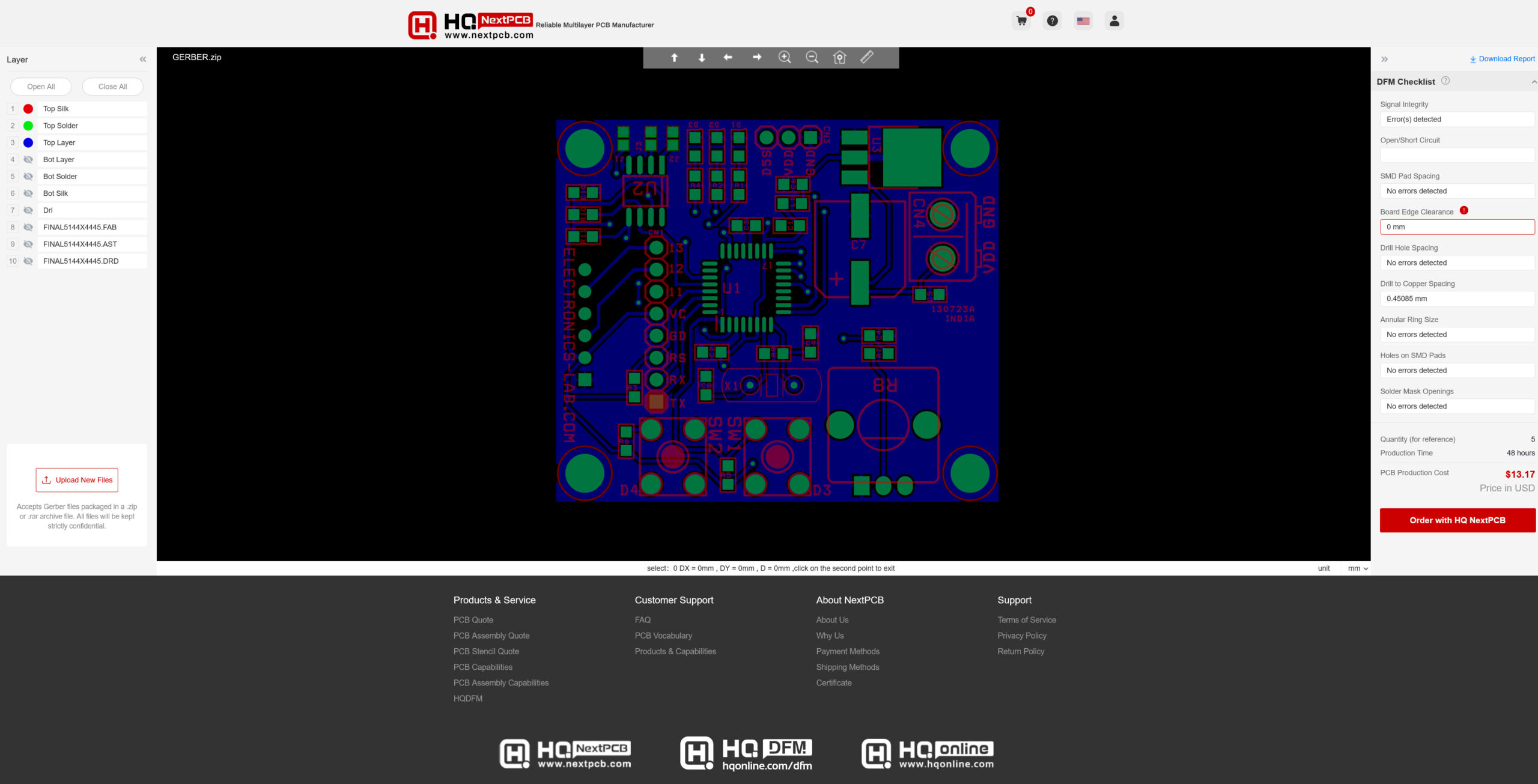
HQ NextPCB is proud to announce the release of HQDFM Online Gerber Viewer and DFM Analysis Tool, free for everyone. With HQDFM, NextPCB hopes to empower designers with the DFM tools and knowledge to perfect their designs as early as possible, where problems are the least costly.
The PCB manufacturing industry has and still relies on the Ucamco Gerber standard to communicate PCB production to manufacturers, which are often located overseas. While the 2D image format overcomes language barriers, the language of PCB Design for Manufacture is still ambiguous to many inexperienced designers and the division between PCB design and PCB manufacture remains an expensive obstacle leading to missed deadlines, hit-and-miss runs and quick-to-fail products.
“There are still many designers that send off their production files without any knowledge of what the files contain. Resolving issues with the fab house becomes a challenge for both sides without the appropriate tools and knowledge to debug the design, which is something we hope to change for everyone’s benefit,” HQ NextPCB CEO, Alex Chen
HQDFM Gerber Viewer is a completely free, online tool for displaying and reviewing PCB Gerber files and OBD++ files. It incorporates HQDFM’s Design for Manufacture (DFM) algorithms based on NextPCB’s 15 years of high-reliability manufacturing expertise and current industry standards.
Unlike EDA software’s built-in DRC checks, HQDFM allows designers to navigate and analyze the production files and check for design issues that may impact manufacturing or cause long-term reliability issues. With HQDFM, designers are given a manufacturer’s perspective and have valuable insights into how they can improve their designs.
Features:
Check for over 20 Design for Manufacture issues
Navigate your PCB layer-by-layer
Free downloadable DFM Report for more detailed analysis
Easy, one-click ordering with HQ NextPCB
Absolutely free, no sign-up or obligation
Based on the free desktop version, the cross-platform, online HQDFM makes the easy-to-use Gerber Viewer function and DFM analysis available to everyone, including Mac and Linux users with no download or installation and no sign-up. Anyone can freely upload PCB production files to the online interface and view their design in seconds.
HQDFM supports X2 and RS-274x PCB Gerber formats, Excellon drill files and OBD++ files and works with Google Chrome, Safari, Microsoft Edge, Mozilla Firefox and Opera browsers.
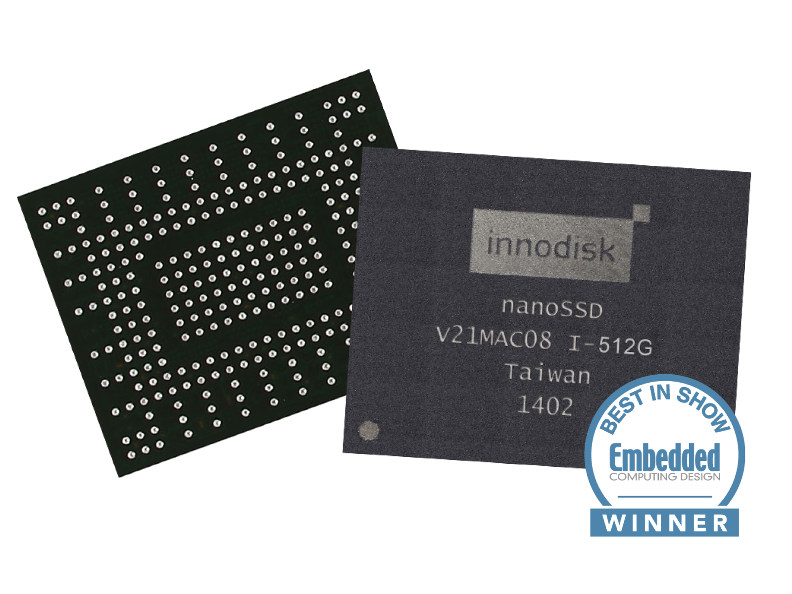
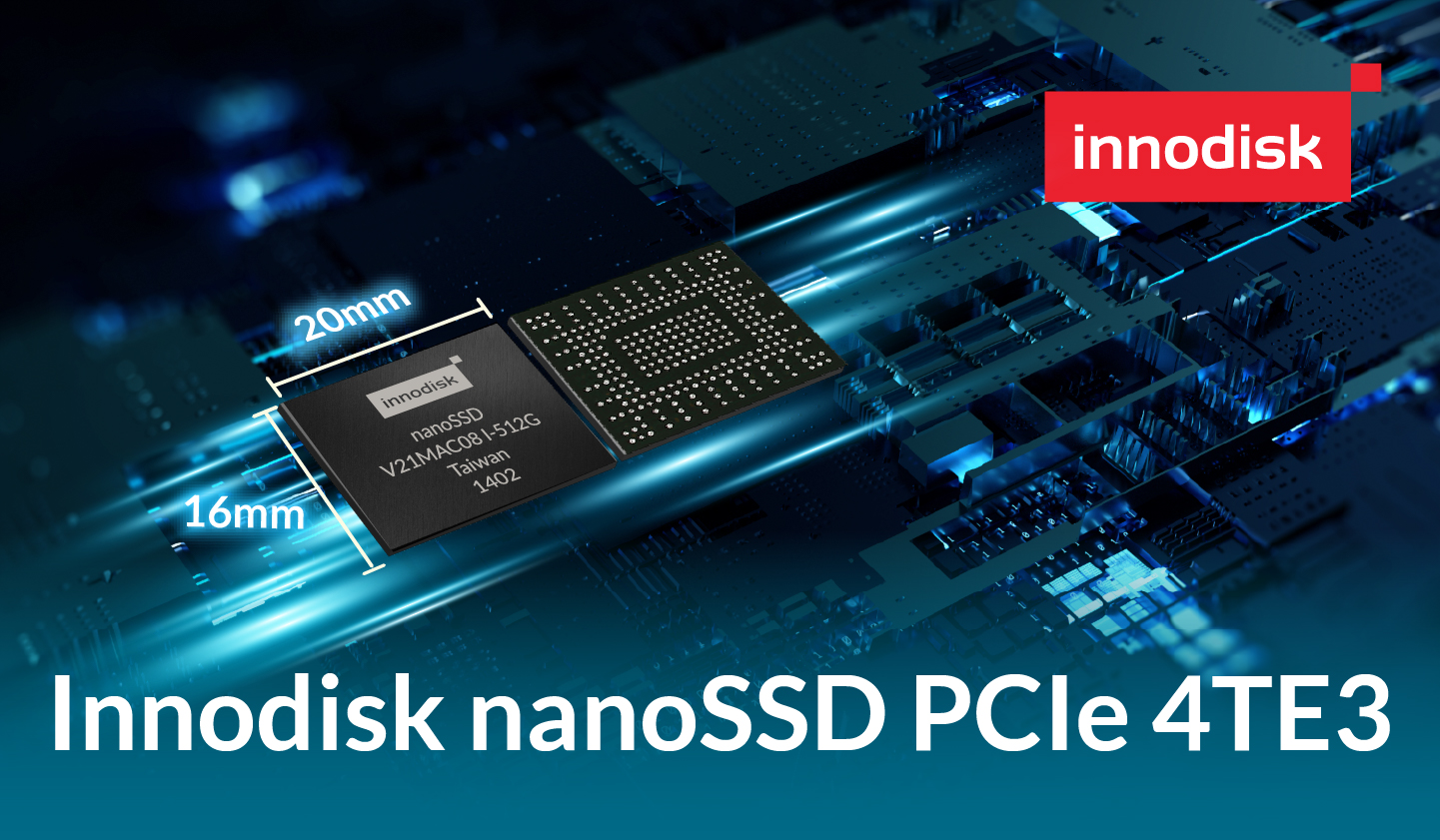
Innodisk, a leading global AIoT solution provider, announces the release of the first nanoSSD PCIe 4TE3 in response to the increasing demands of edge AI miniature design and high computing performance.
The nanoSSD 4TE3 is a PCIe 4.0 x4 BGA SSD featuring compact size, enhanced performance and reliability to unlock the potential for 5G, automotive and aerospace applications.
Enhanced Performance with Tiny Size
Edge AI devices often demand efficiency and substantial capacity within a minimal space and are positioned in rugged external environments. These devices installed at, for example, 5G base stations, aerospace and in-vehicle systems require a small size to save space in devices with large capacity to support AIoT applications. Innodisk’s nanoSSD PCIe 4TE3 emerges as a solution designed in M.2 type 1620 BGA form factor with a height of only 1.65mm but with large capacity reaching up to 1TB, which is suitable for the needs of space-limited devices and increasing design flexibility. Beyond this, the nanoSSD offers high performance with a transmission speed of up to 3.6GB/s and a bandwidth of up to 8GB/s catering to high-speed computing needs.
By employing 12-nanometer controller and a 112-layer 3D TDC NAND Flash, the nanoSSD PCIe 4TE3 performs optimized efficiency and reliability, as well as low power consumption and reduced heat energy, contributing to a small footprint for sustainability. Furthermore, the PCIe 4TE3 comprises Innodisk’s iSLC technology extending its lifespan by 33 times to fulfill high performance demands and the needs for embedded and most industrial applications, providing high endurance and reliability.
Tailored Solutions for Design Flexibility
Unlike conventional plugged-in SSDs, the nanoSSD is solder-down and integrated onto the device motherboard against instabilities in outdoor environments, such as shaking and vibrations, ensuring uninterrupted signal and operation. At the same time, the circuit design is supported by pre-sales service, including a design kit before integration. The series is designed in-house, which brings advantages to enhanced quality and highly customized solutions for flexibility. Further customized options, including namespace and security features, are designed to align with specific requirements. For instance, namespaces enhance storage allocation flexibility, while security features such as AES-256, TCG Opal, quick erase and write protection can be added for mission critical applications where security safety is crucial.
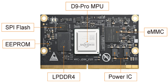
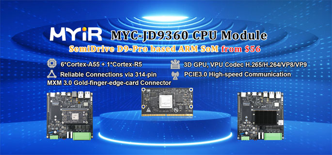
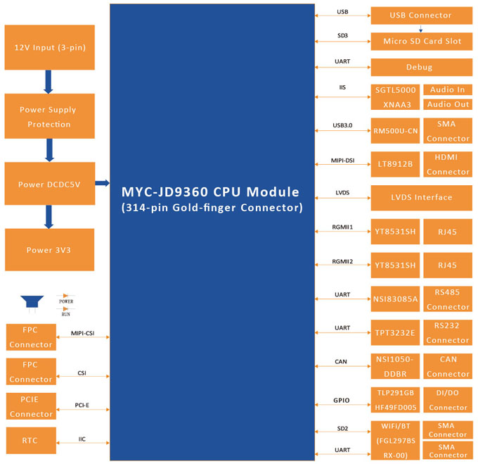
MYIR has launched a new ARM SoM MYC-JD9360 CPU Module based on the intelligent industrial processor D9-Pro (D9360) from SemiDrive, equipped with six high-performance Arm Cortex-A55 cores (up to 1.6GHz) and one dual-core lockstep high real-time and high-reliability Cortex R5 core (800MHz). In addition to the D9-Pro MPU, the MYC-JD9360 CPU Module has integrated 2GB LPDDR4, 16GB eMMC, 16MB QSPI Flash, 256Kbit EEPROM, Watchdog timer chip and Isolated power supply. It carries out a variety of peripherals and IO signals through the0.5 mm pitch 314-pin gold-finger-edge-card expansion interface including TSN-enabled Gigabit Ethernet, USB3.0, PCIe 3.0, SDIO, UART, I2C, SPI, ADC, CAN FD, MIPI-DSI, MIPI-CSI, LVDS, etc. It also takes advantage of the D9-Pro processor to support high-performance 3D graphics processing,high-efficiency AI accelerator, and high-definition visual processing. This enables the MYC-JD9360 module to be seamlessly connected and applied to various industrial applications at an affordable cost. Typical applications are industrial robots, engineering machinery T-BOX, intelligent cockpits, in-vehicle entertainment, intelligent medical equipment, and so on.
MYC-JD9360 CPU Module
The MYC-JD9360 CPU Module measures 82mm by 45mm. It is capable of running multiple different operating systems including Linux, Ubuntu, and Android OS. The module is provided with plenty of software resources including but not limited to, bootloader, kernel, drivers, images, and relative development tools, together with a detailed user manual and documentation to help customer start their development rapidly.
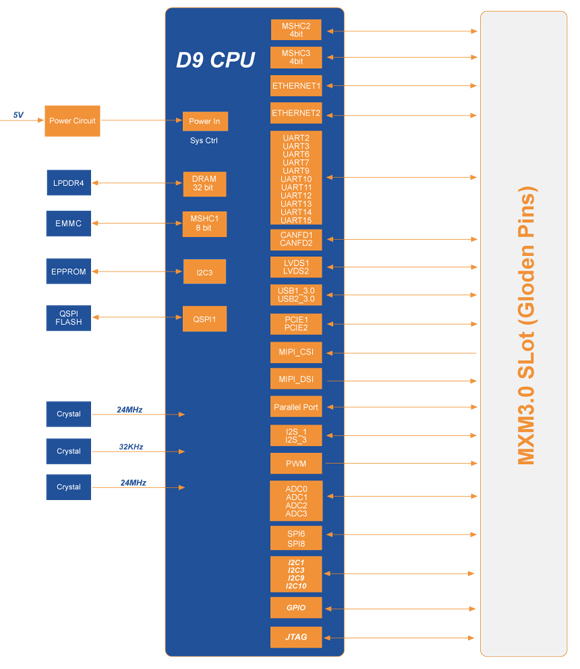
MYC-JD9360 CPU Module Block Diagram
Features of MYC-JD9360 CPU Module
Dimensions: 82mm x 45mm
PCB Layers: 8-layer design
Power supply: 5V/5A
Working temperature: -40~85 Celsius (industrial grade)
* Up to 135x GPIOs (Note: the peripheral signals brought out to the expansion interface are listed in maximum number. Some signals are reused. Please refer to the processor datasheet and CPU Module pin-out description file.)
Linux
Ubuntu
Android (coming soon)
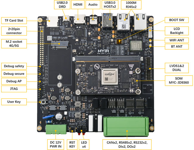
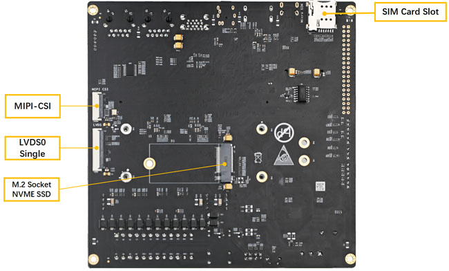
The MYD-JD9360 Development Board is a starter kit for evaluating the MYC-JD9360 CPU Module. It has a versatile base board to facilitate the expansion from the MYC-JD9360 through the 314-pin expansion interface, a rich set of peripherals and interfaces have been brought out such as two RS485, two RS232, two CAN, two Gigabit Ethernet, two USB Host, one DRD, one USB based 5G/4G module interface and one WiFi/BT module. It also has advanced multi-media capabilities to support dual LVDS display, audio and camera, and HDMI display support via MIPI-DSI. The MY-CAM003M MIPI Camera Module and MY-LVDS070C LCD Module can be used as options for the MYD-JD9360 board which allows customers to acquire a better development experience. It is an excellent reference design for using D9-Pro solutions.
MYD-JD9360 Development Board (top-view)
MYD-JD9360 Development Board (bottom-view)
MYD-JD9360 Development Board Block Diagram
The MYC-JD9360 CPU Module is priced at only $65/pc. Discount is to be offered for volume quantities. MYIR also provides OEM/ODM services to help customers accelerate their time to market and save costs.
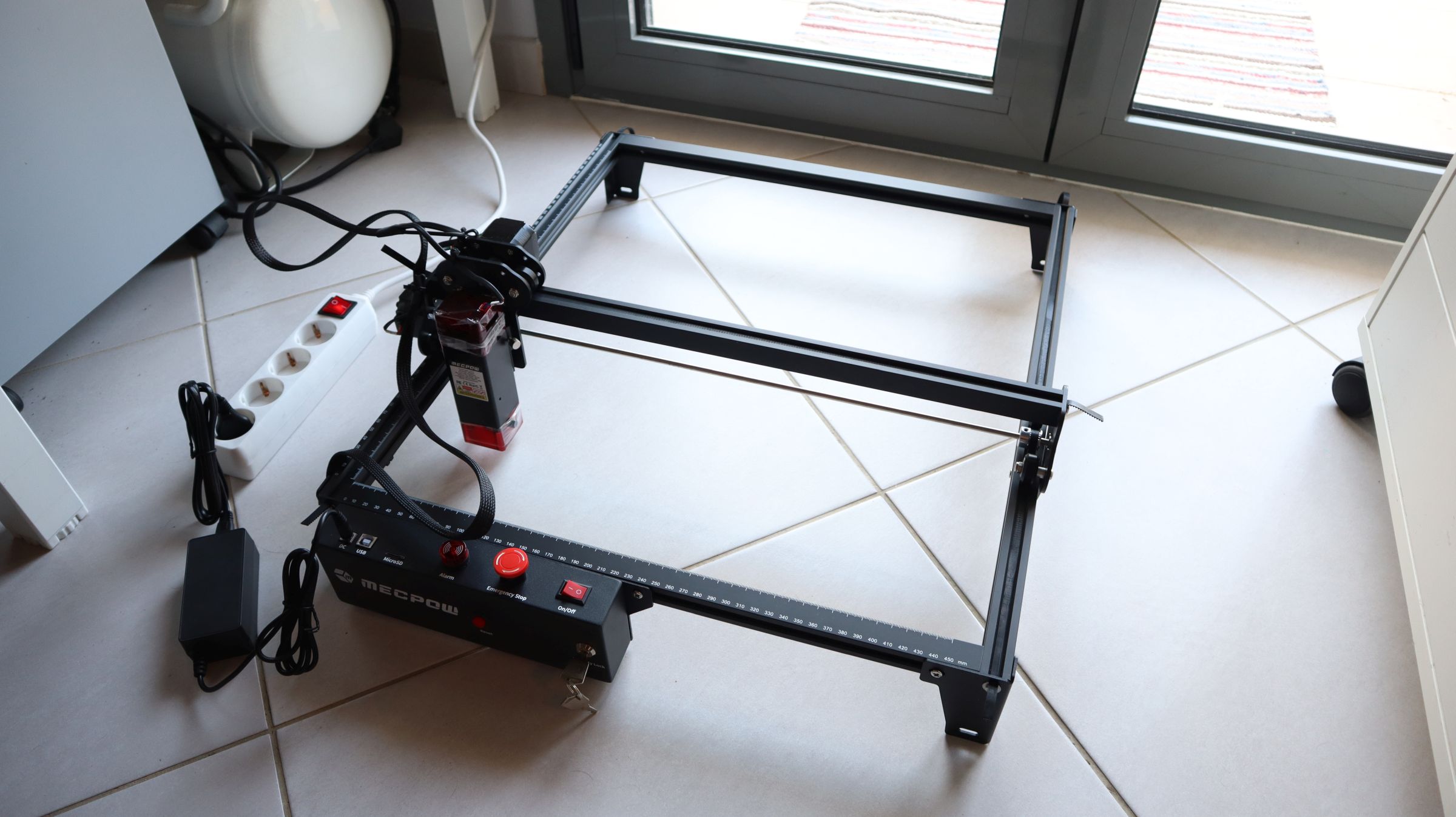
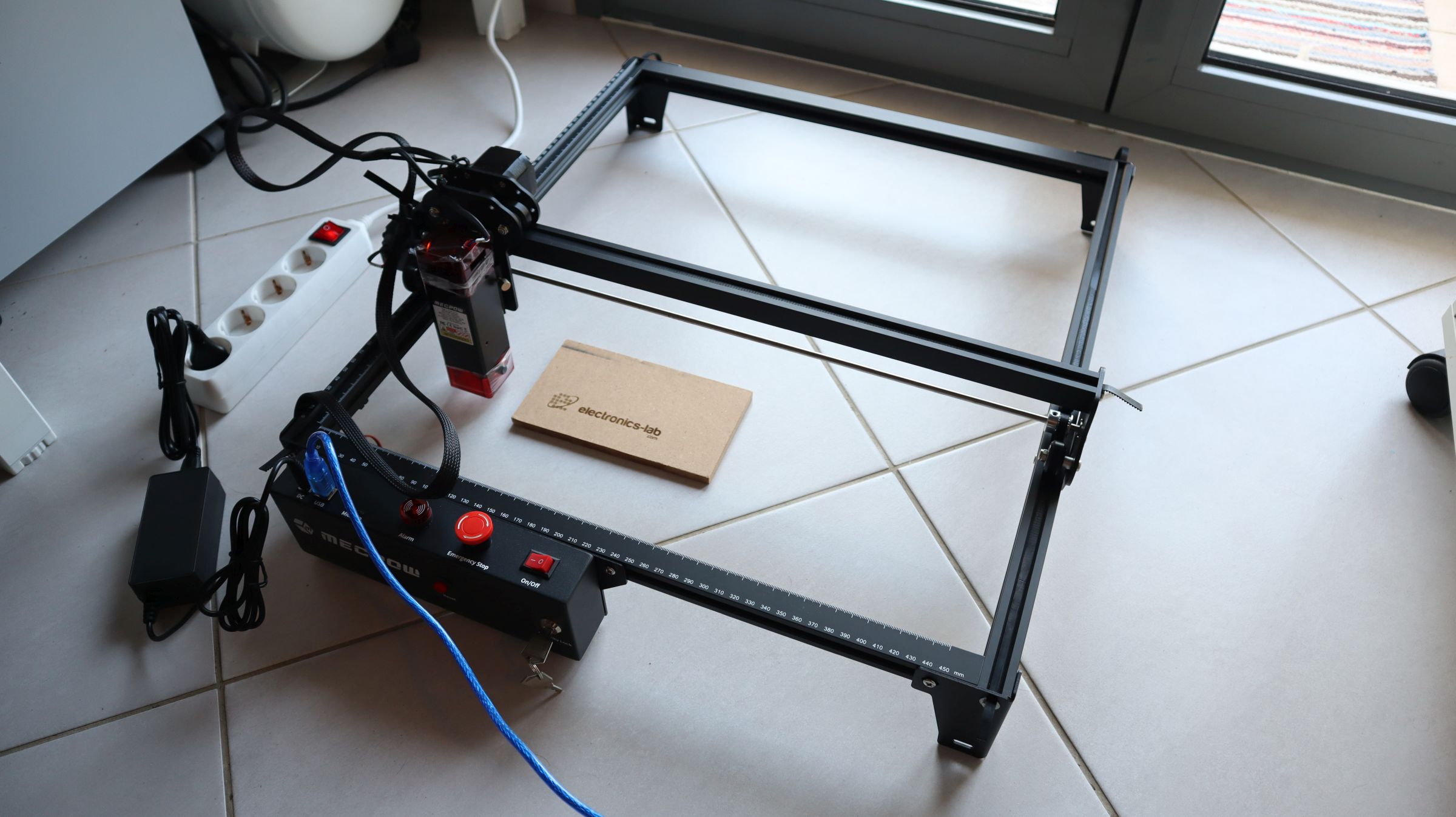
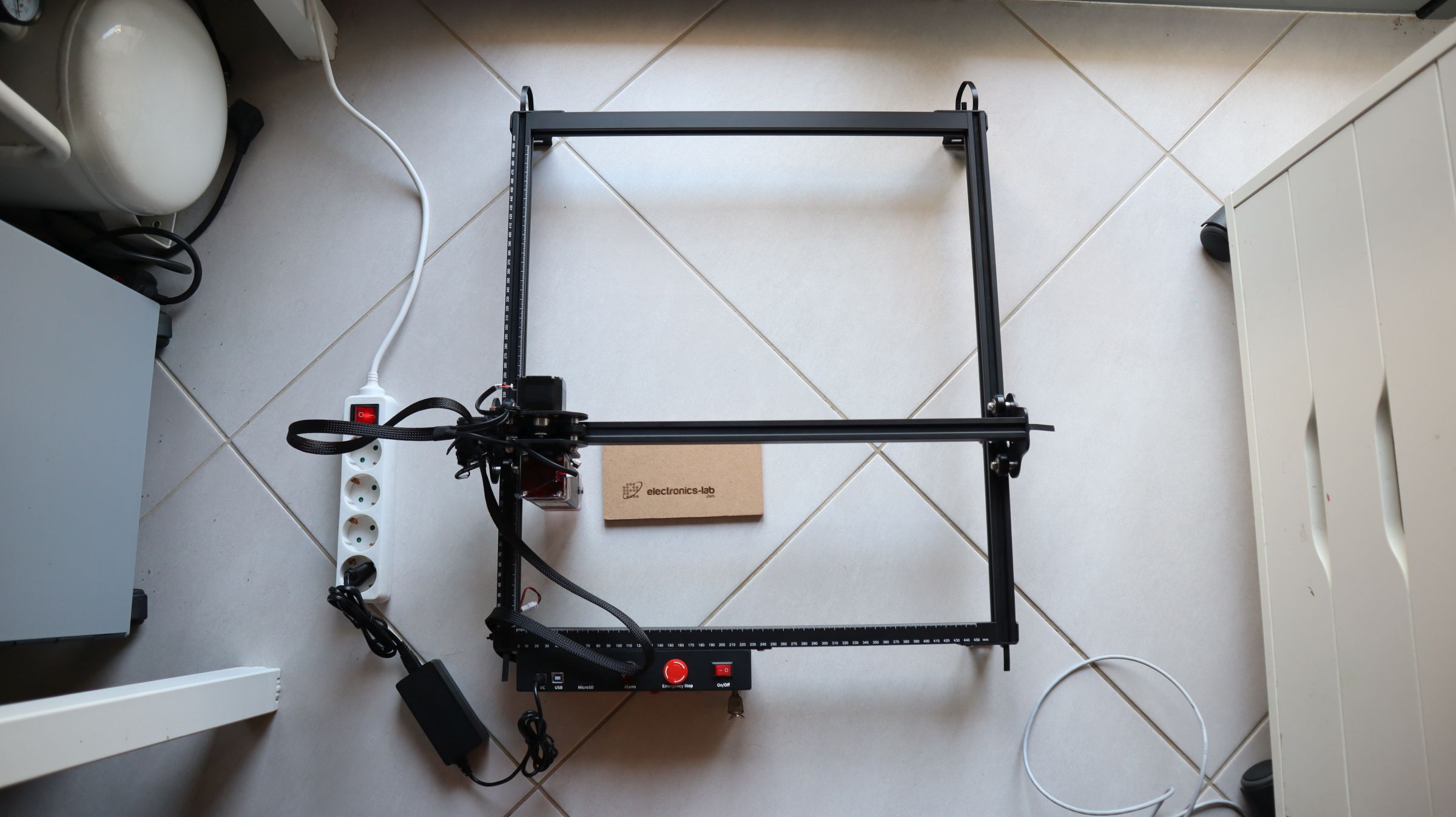
Whether you’re a hobbyist, a businessowner, or a DIY enthusiast, a laser engraver becomes a convenient tool if you are into creating custom designs. It allows you to develop custom-engraved products using various materials, such as wood, acrylic, leather, fabric, and even certain types of metal. But with so many models in the market, sometimes it becomes tough to figure out which is the best for you, so we want to introduce you to Mecpow X3 Pro, a module laser engraver with an extendable engraving area.
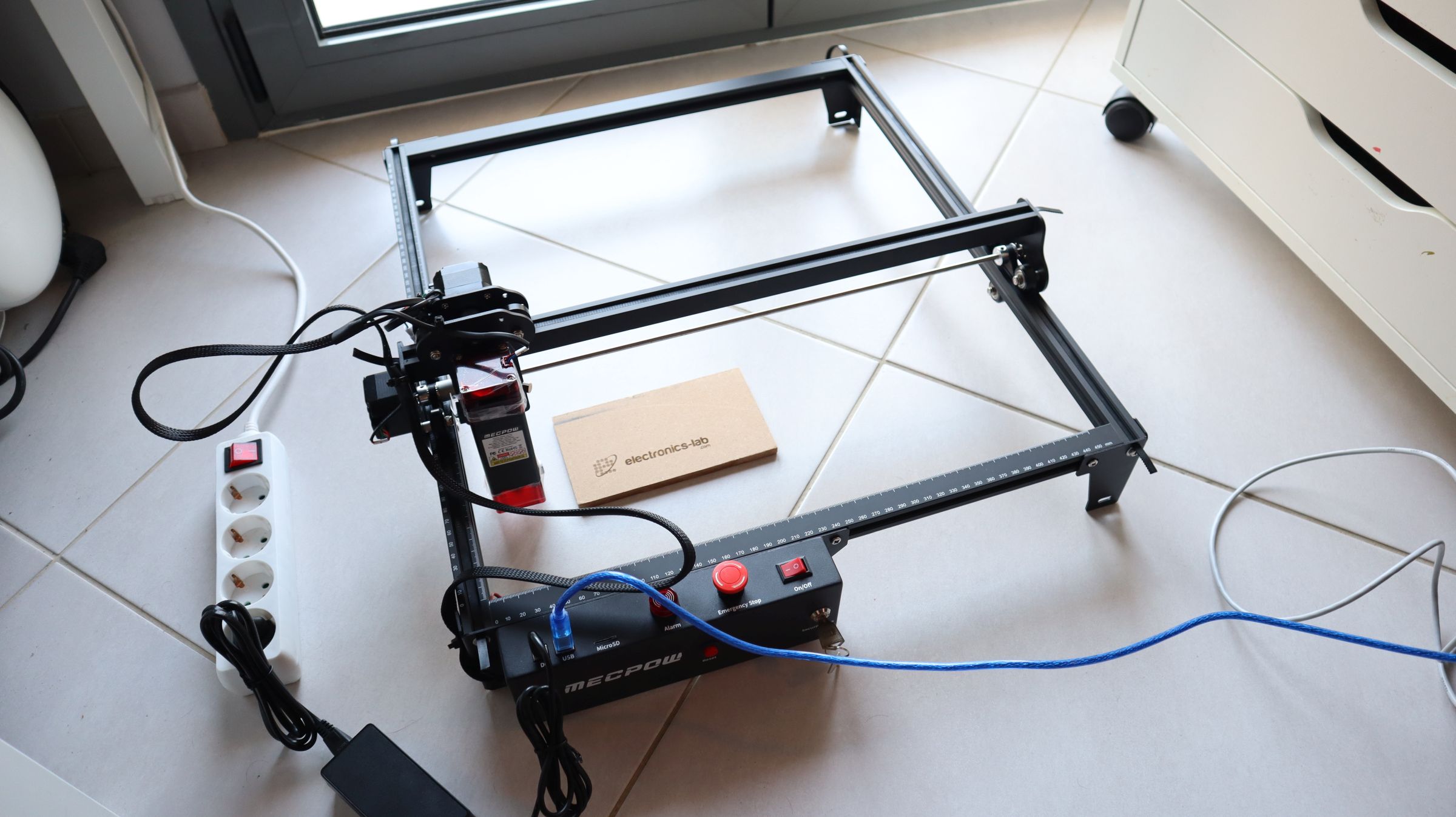
Yes! You read that right; this engraver has an extendable engraving aria, the standard dimension of 400mm x 410mm, but with some modification, it can extend up to 400mm x 750mm. That is a massive boost for your projects. It also has an air assist and pump, precision stepper motors, a large extendable engraving area, and user-friendly software support. All these features make the Mecpow X3 Pro an extraordinary tool for your engraving projects while offering remarkable value for its price.
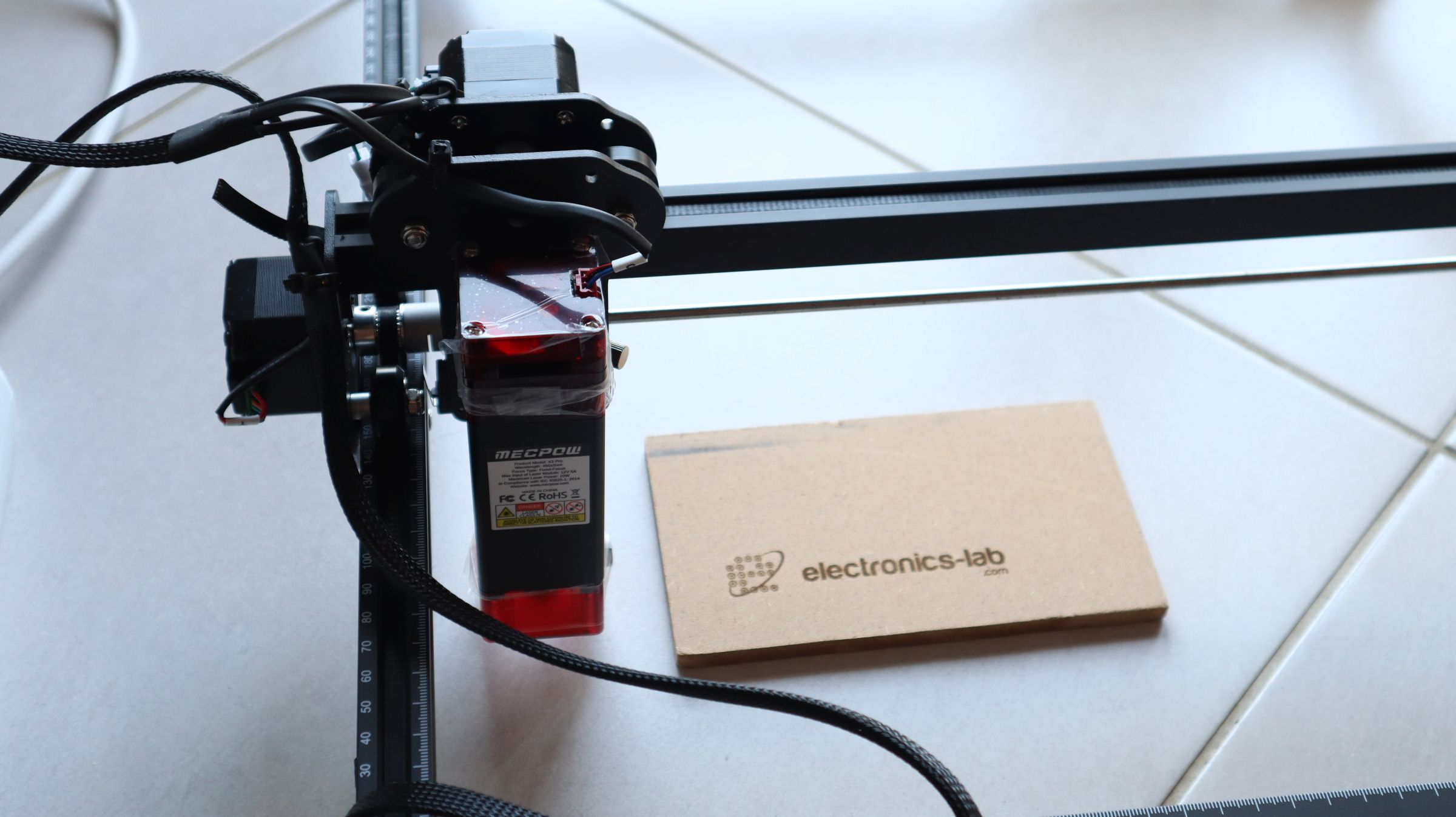
The Laser Diode
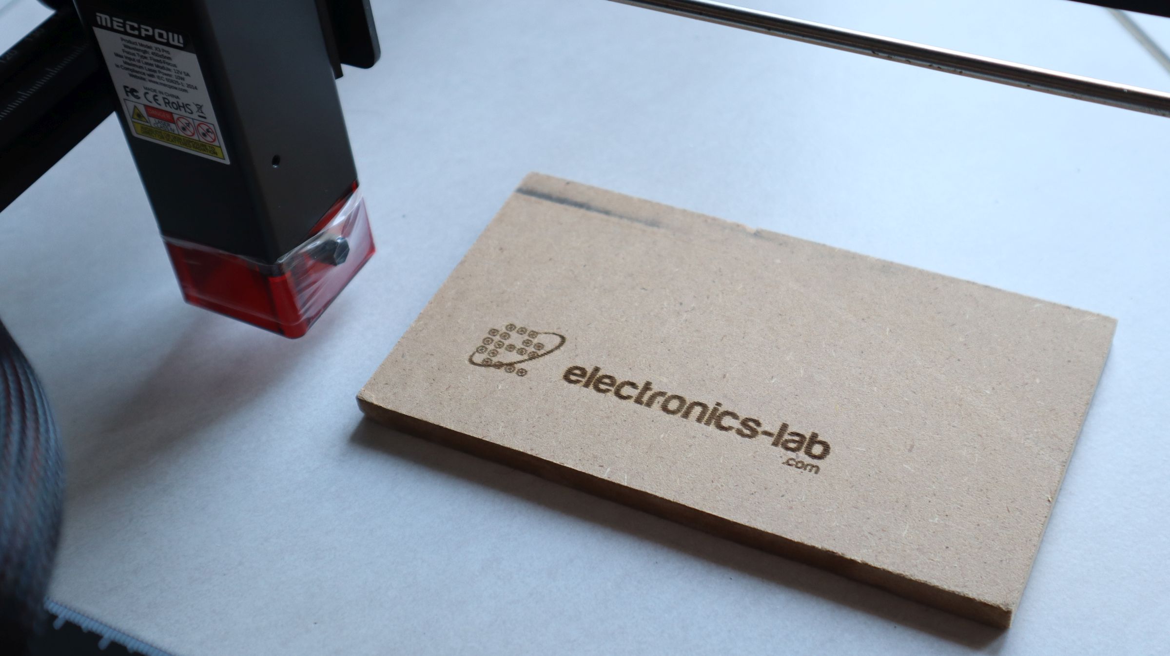
The Mecpow X3 Pro has a powerful laser diode that can output up to 10W of laser power. The laser diode is a fixed-focus diode which means it’s reliable and almost maintenance-free. Additionally, it claimed to have a rectangular beam spot shape of 0.08mm x 0.06mm, which is impressive compared to other lasers in this category.
Fixed focus means no moving parts in the laser, unlike those which use mirrors and reflectors to divert the laser beam. That also means the beam width is narrower, and the engraver is almost maintenance-free.
It’s also shocking to see how small the laser head is compared to other laser engravers. Because of that, this engraver can reach an engraving speed of 100,000 mm/min, which is very high compared to others. But the most fascinating thing about this engraver is its engraving accuracy of 0.01mm. That is game-changing because a fast engraver tends to lag precision.
This laser cutter houses a powerful 10W laser that can cut various materials. For instance, it can cut 20mm pine wood, 15 mm black acrylic, and even 0.1 mm stainless steel in a single pass. It can do multiple passes to cut thicker materials and still produce a clean cut thanks to its revolutionary 0.01mm accurate laser beam.
The Focusing Procedure
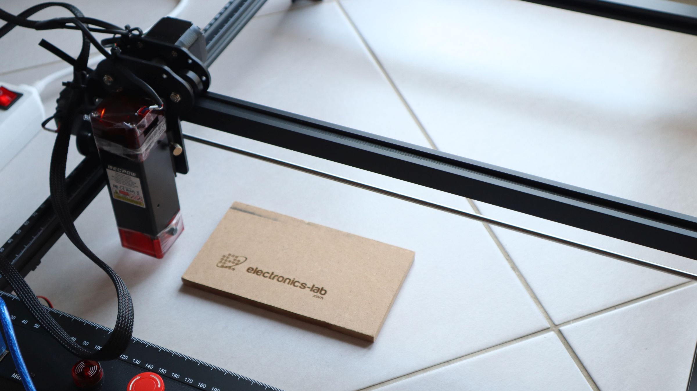
One of the pain points of any laser engraver is its focusing process; that is why the developers of Mecpow came up with a unique workaround, and it’s done with the help of the included focusing plate.
To adjust the focus, you place the focusing screen on top of the object now move the laser head down until the laser head touches the focusing plate, and your focusing is done. That’s how easy it is to do the focus for this machine.
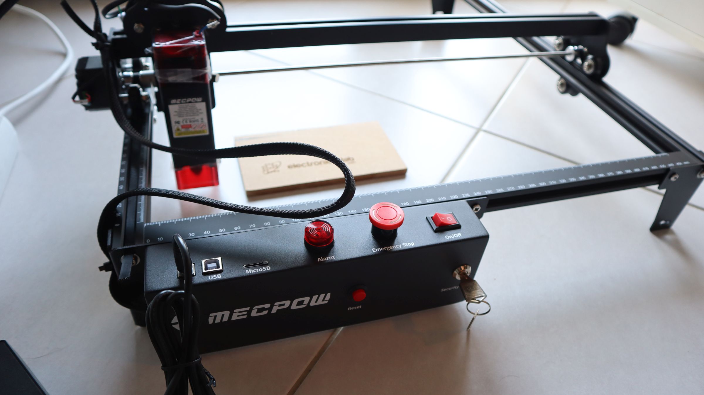
Special Features and Safety Measures
This laser engraver/cutter includes various special features, like Extendable Engraving Space, an Eye Protector shield, Air Assist, and more. It also includes safety features like Emergency Stop Button, Limit Switches, Fire Sensor, Alarm, and more.
Extendable Engraving Area
This engraver’s most interesting takeaway is its ability to expand its engraving area. The engraver has a standard engraving space of 400mm x 410mm, but with a kit, you can increase it to 750mm x 400mm.
It also features a built-in laser shield for better eye protection. The built-in laser shield filters out 98% UV light to protect your eyes. You will get a pair of laser safety glasses in the box for additional eye protection.
The Air Assist Pump
The Mecpow X3 Pro offers a fully controllable air assist pump that can be turned on and off automatically or controlled through Lightburn. The air assist pump increases cutting precision and quality by removing debris and smoke for a clear cut. It also blows out the additional combustible gasses, reducing the fire risk.
Other safety features include a Flame Sensor, an emergency stop button a gyroscope sensor to detect tilt. If the machine tilts more than 50±5°, the control board stops the machine to prevent damage. It also features a Security lock and bump protection for added security.
The limit switch feature is the best feature a laser engraver could have. With a limit switch, you can set a home command, and the printer head will go to the home position, just like a 3D printer would. It also helps a machine start from the same place every time, even after interruptions.
Software Support
The Mecpow X3 Pro is compatible with the free LaserGRBL software, though it can be somewhat laggy. I prefer LightBurn, which is well-organized and intuitive. However, LightBurn isn’t free. After a 1-month trial, there’s a $60 license fee. Despite the cost, it’s valuable because it significantly saves time.
With LaserGRBL, you can import vector files (NC, BMP, JPG, PNG, DXF…) and bitmap image files (BMP, jpg, png and gif), but with Lightburn, you have support for more formats like AI, SVG, DXF, PDF, HPGL, PLT, and RD for vector formats and PNG, JPEG, BMP, TIFF, TGA, and GIF for image formats.
For any laser engraver, a vector file is preferred because it guides the laser along the shape’s edges directly. This is faster than the dot-making method used for bitmap images.
You can find many free vector designs online and use programs like Inkscapeor QCADto create them. Additionally, you can download free vectors or purchase unique designs from sites like Etsy to enhance your work.
The laser engraver comes with various tools and accessories to get you started. You will get an air assist pump, user manual, adapter, controller, screws, screwdriver, Allen key, brackets, aluminum guide rods, and more in the box. All these components together provide a seamless engraving experience.
If you’re interested in purchasing the Mecpow X3 Pro 10W Laser Engraver with Air Assist Kit, you can use any of the links above. In any case, the price will be $279.99 no matter the platform choice. Don’t miss out on this great deal!
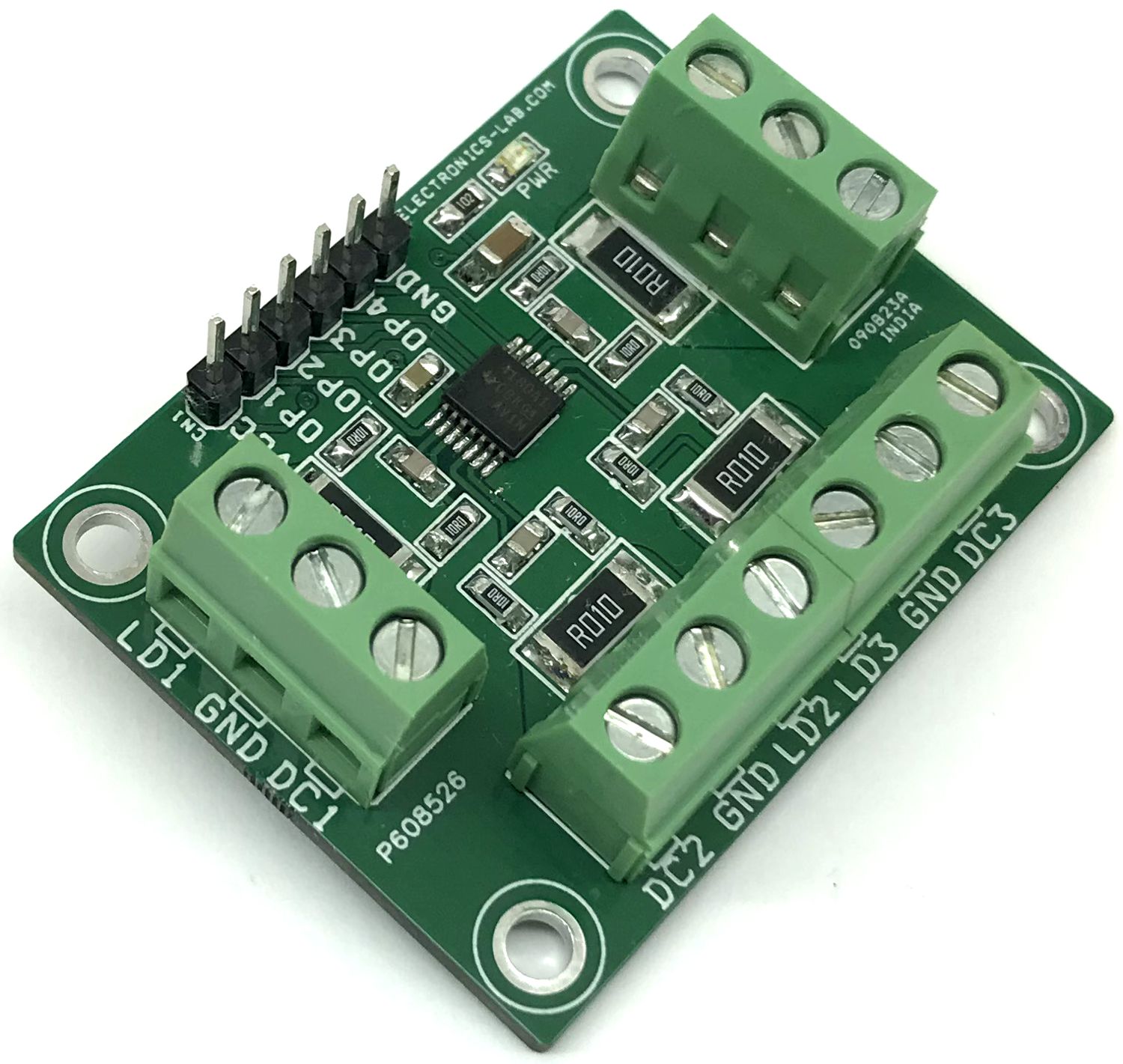
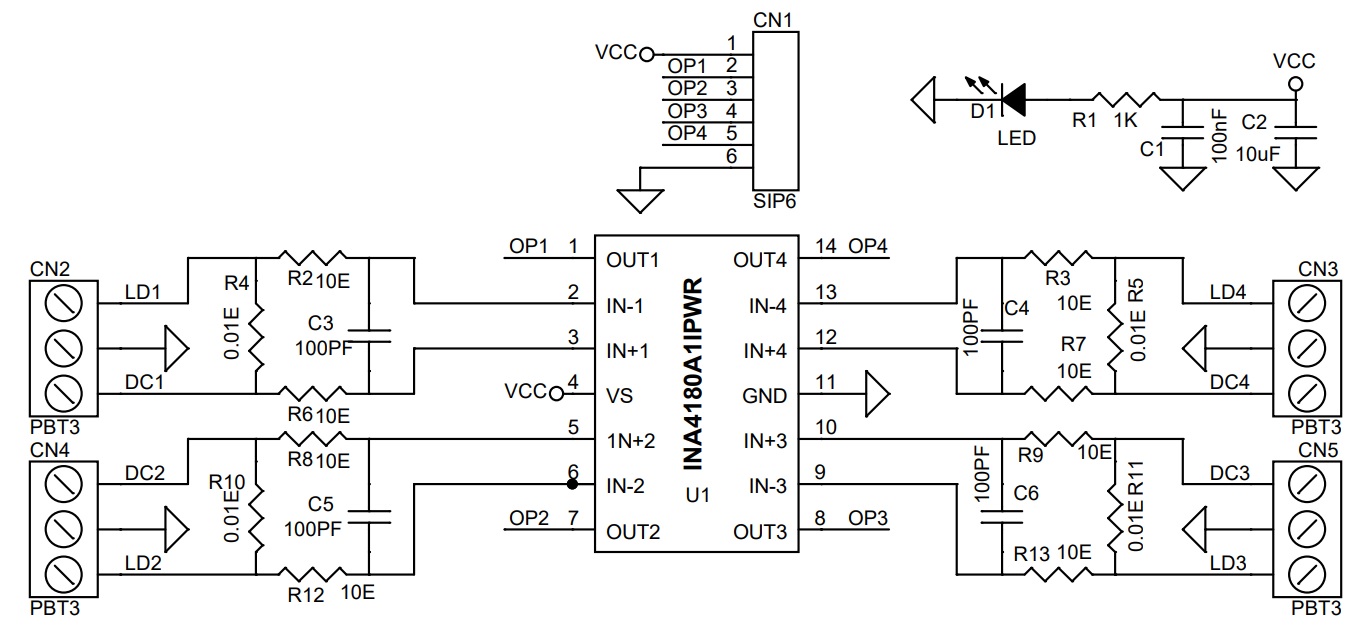
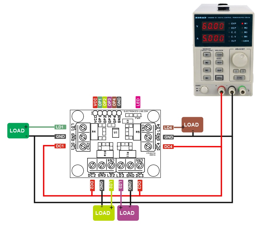
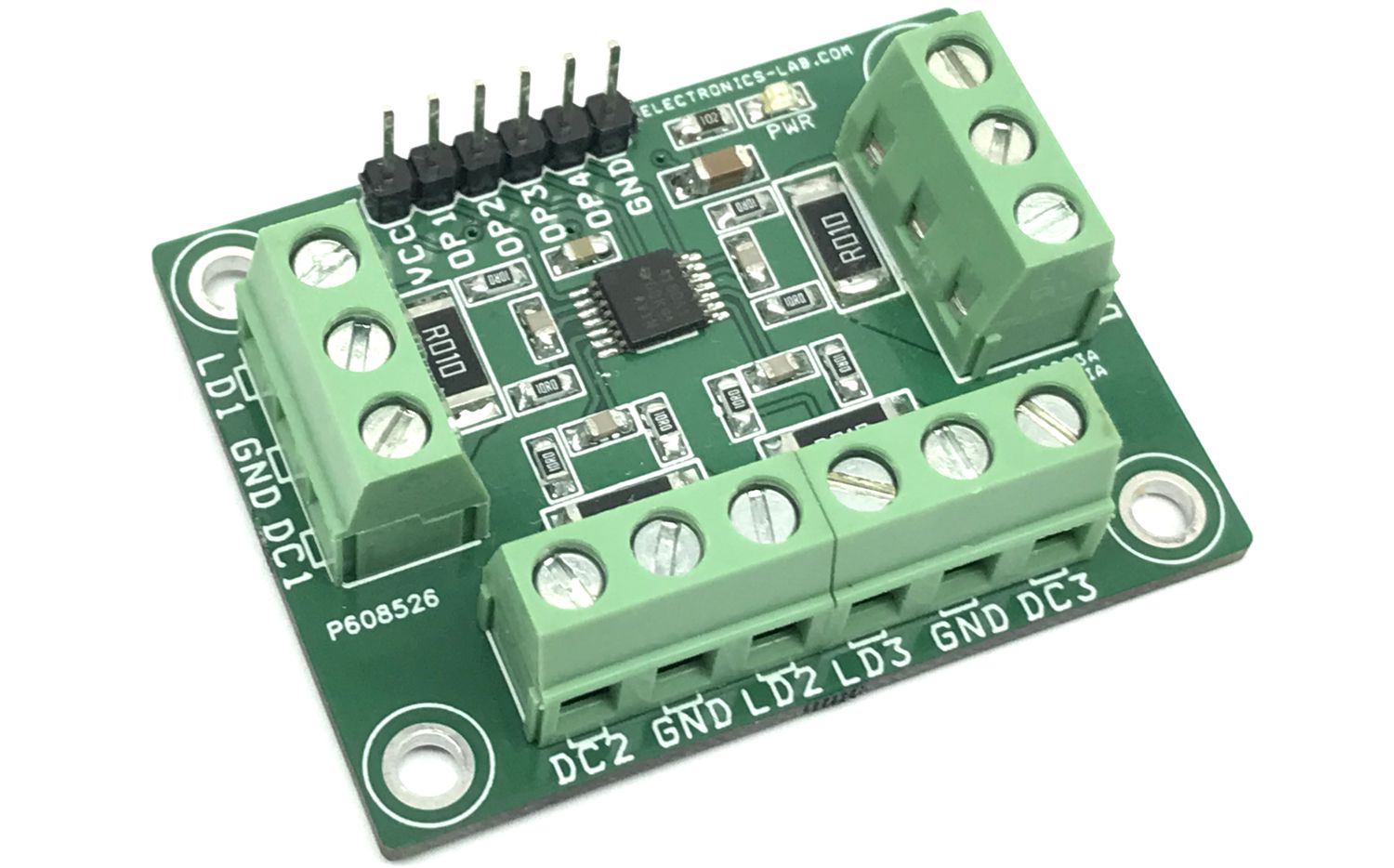
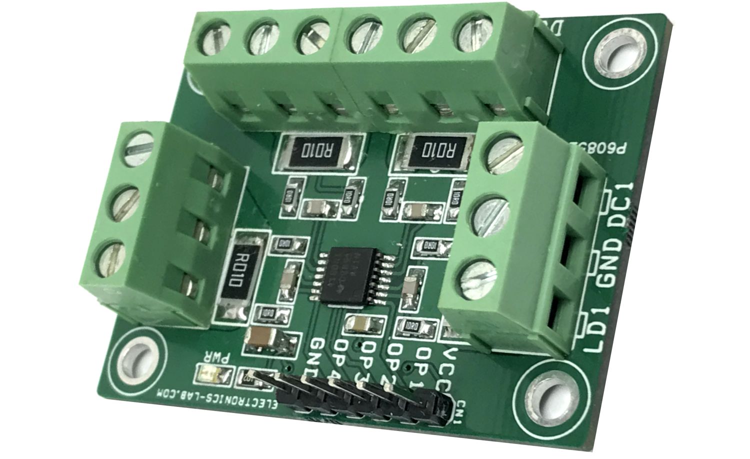
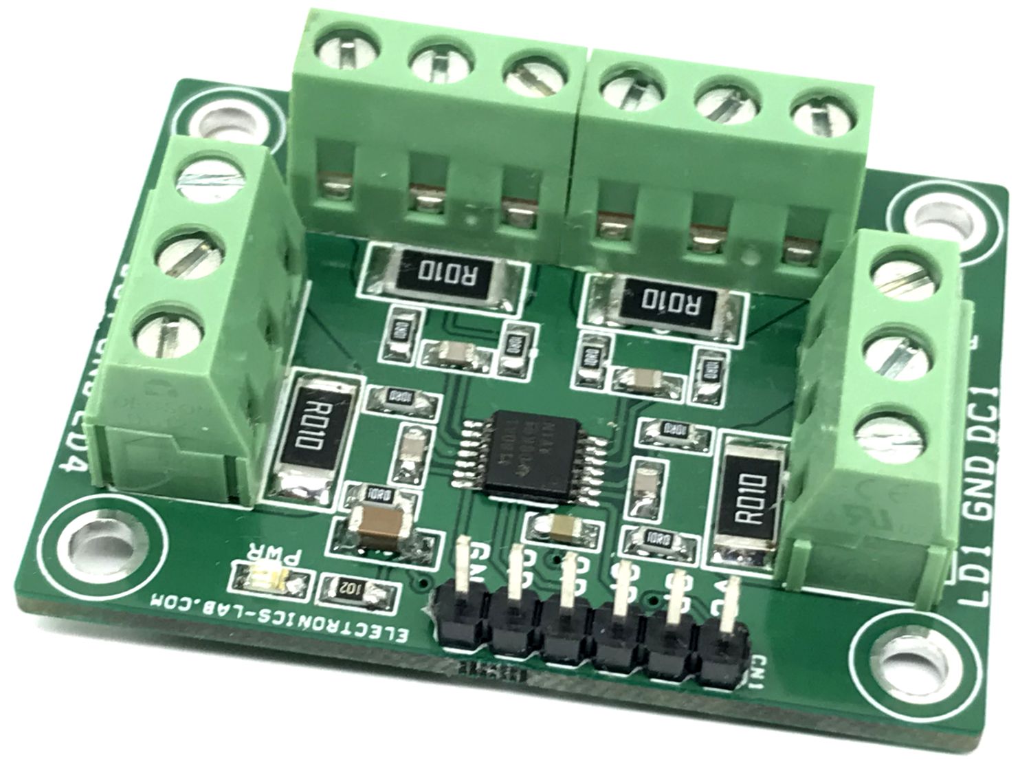
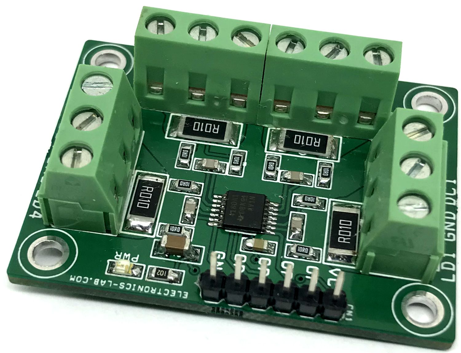
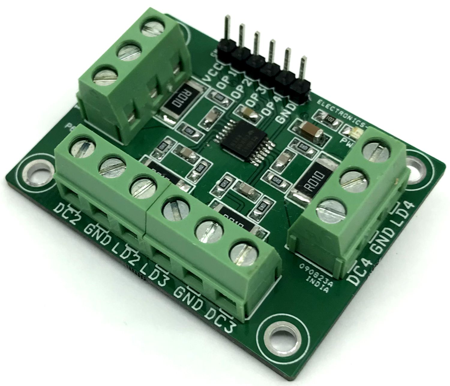
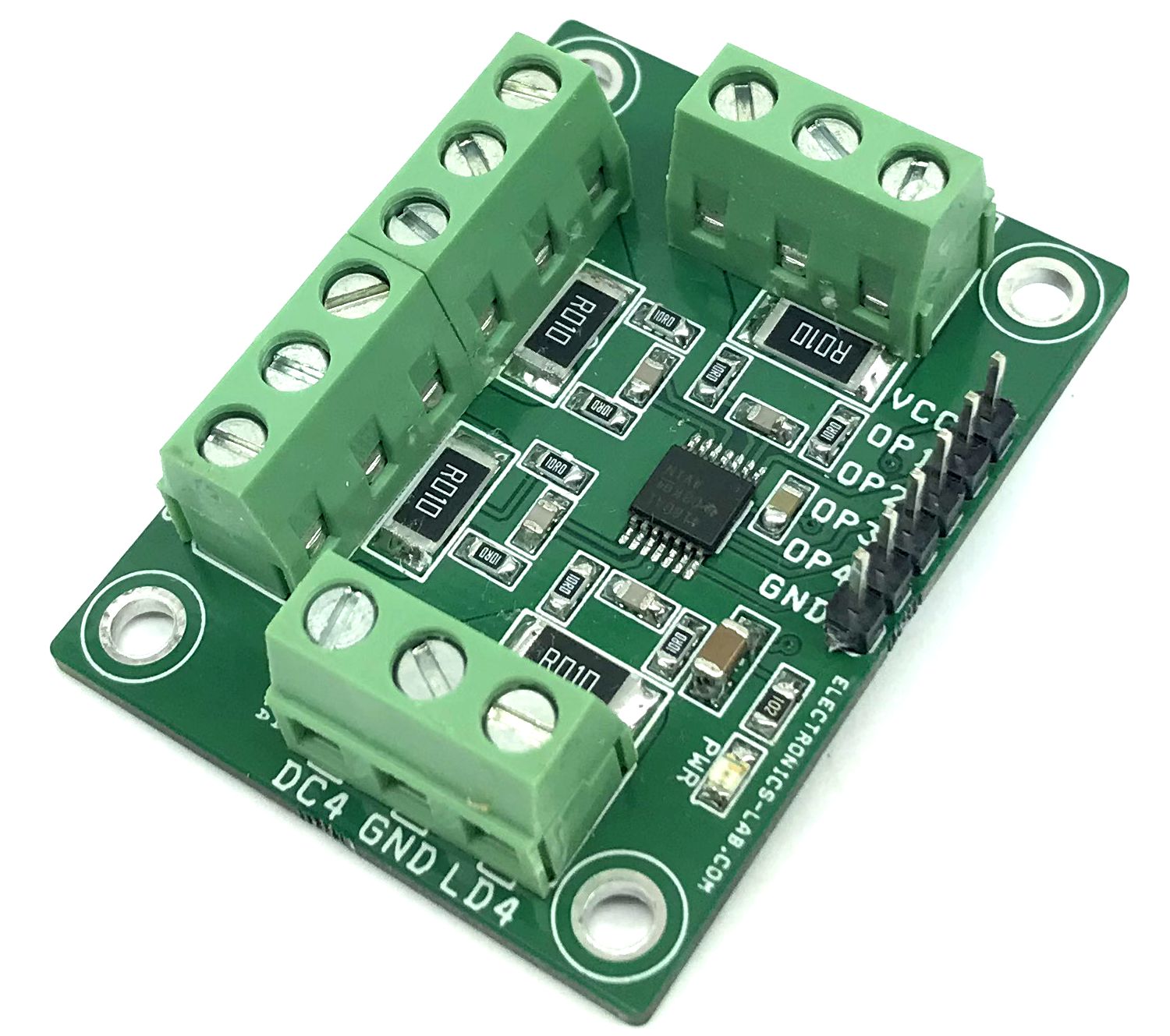
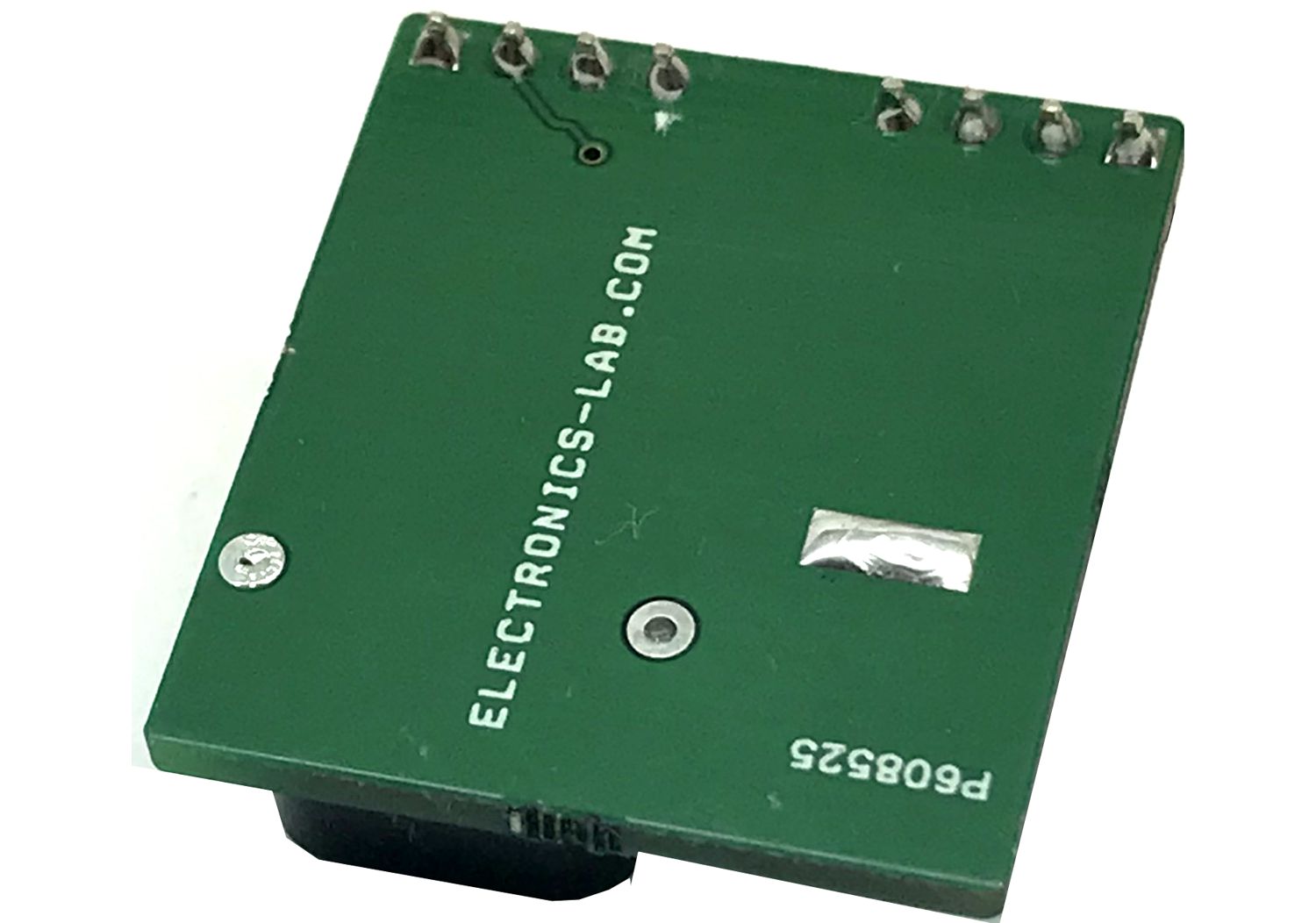
This 4-Channel current sense amplifier is designed for cost-optimized applications. This is a current-sense amplifier (also called a current-shunt monitor) that senses the voltage drop across current-sense resistors at common-mode voltages from –0.2 V to +26 V, independent of the supply voltage. The project was built using INA4180 chip which integrates a matched resistor gain network in four, fixed-gain 20V/V, this matched gain resistor network minimizes gain error and reduces the temperature drift. The board operates with a single 2.7-V to 5.5-V power supply. The four-channel INA4180 draws a maximum supply current of 900 µA. Resistors R2, R6, R8, R12, R3, R7, R9, R13 and Capacitor C3, C4, C5, C6 used as input filters. The gain of the amplifier is 20V/V, and external input resistors resulting a 0.9% gain error.
Gain Selection
INA4180A1 Gain 20V/V
INA4180A2 Gain 50V/V
INA4180A3 Gain 100V/V
INA4180A4 Gain 200V/V
Gain: The board is populated with an INA4180A1 chip that has a gain of 20V/V, the user may choose any of the above chips with a higher gain.
Note: Shunt Resistor 0.01Ω with 20/V Gain Amplifier, Output = 0.2 V/A + Input Filter Circuit Error
The project is tested with 4 x 0.01Ω/3W current resistors, considering approx. current sense range up to 10A. The users may choose the appropriate current sense resistor and Amplifier with different gains as per requirement. Refer to the datasheet of the chip for more info. The accuracy of the INA4180 is maximized by choosing the current-sense resistor to be as large as possible. A large sense resistor maximizes the differential input signal for a given amount of current flow and reduces the error contribution of the offset voltage. However, there are practical limits as to how large the current-sense resistor can be in a given application. The INA4180 has a typical input bias current of 80 µA for each input when operated at a 12V common-mode voltage input. When large current-sense resistors are used, these bias currents cause increased offset error and reduced common-mode rejection. Therefore, using current-sense resistors larger than a few ohms is generally not recommended for applications that require current-monitoring accuracy. A second common restriction on the value of the current-sense resistor is the maximum allowable power dissipation that is budgeted for the resistor.
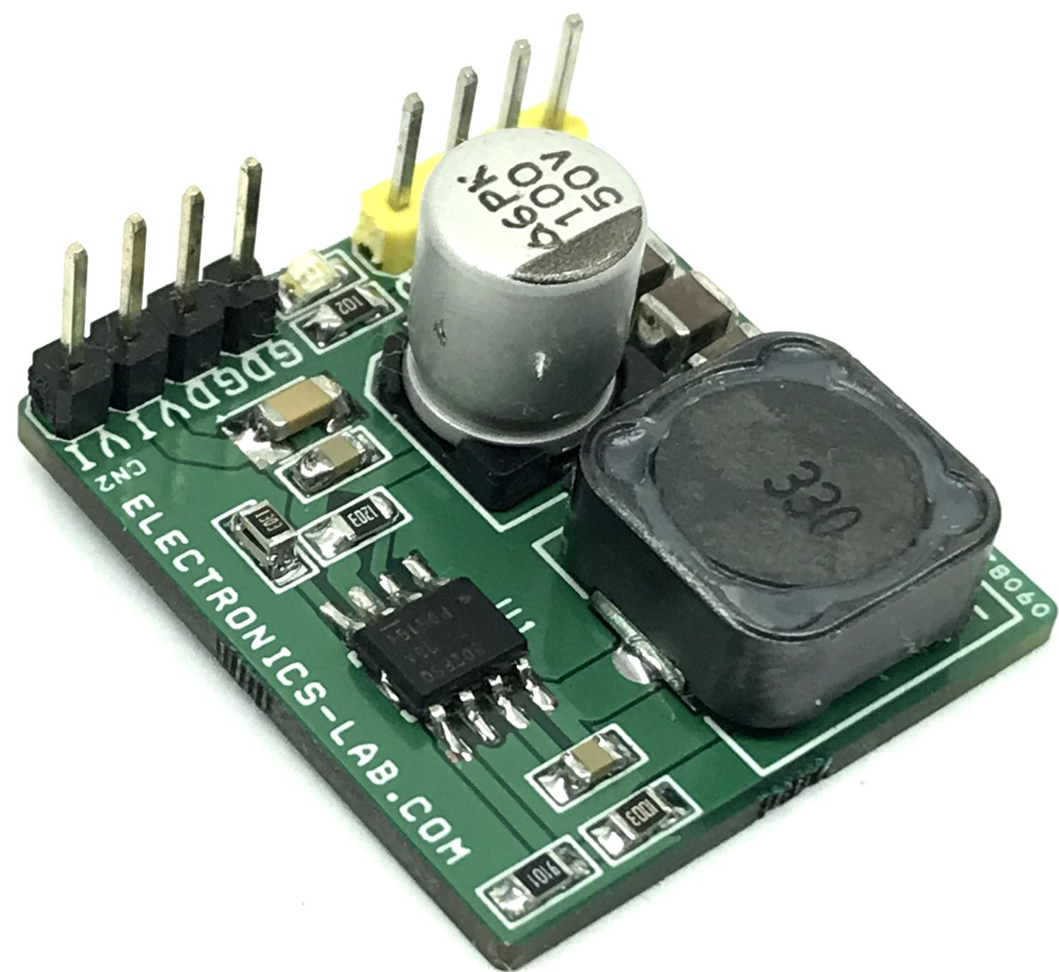
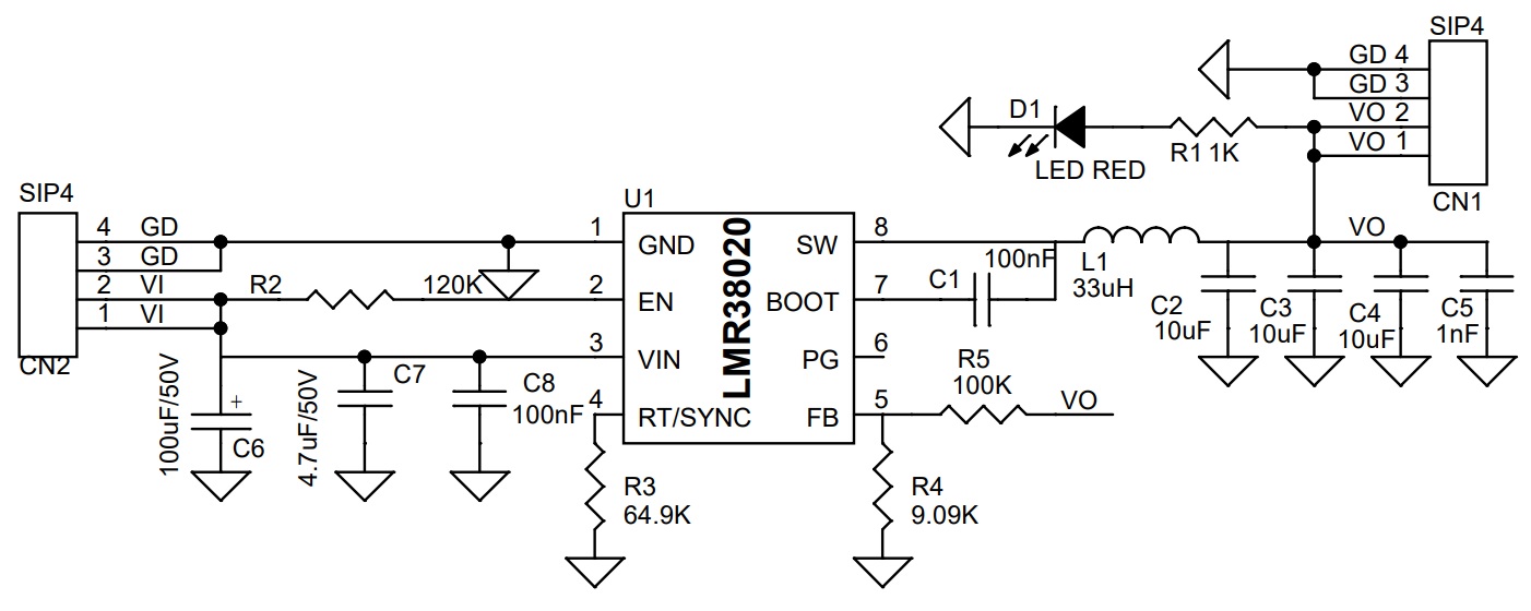
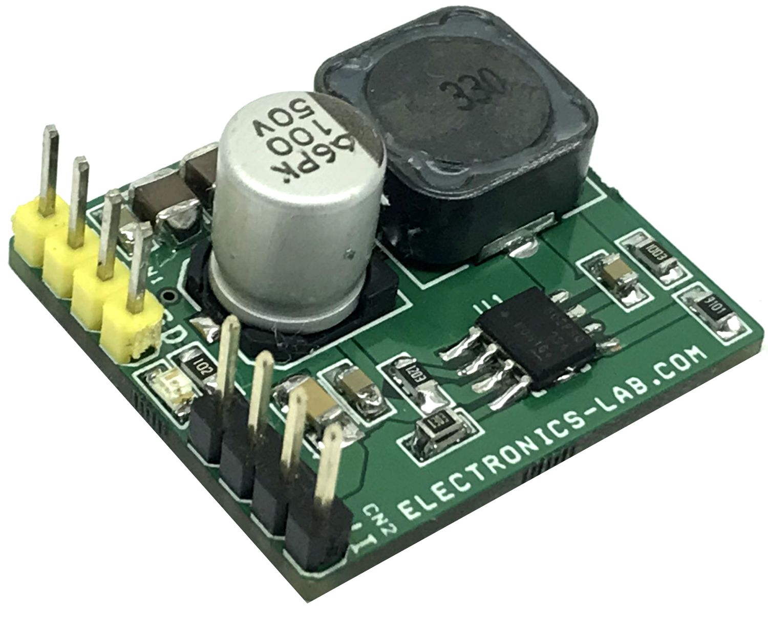
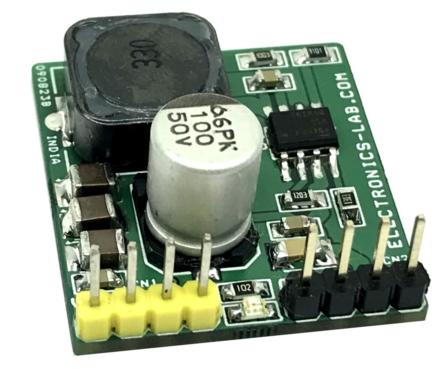
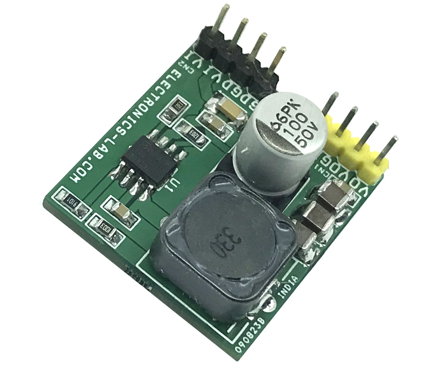
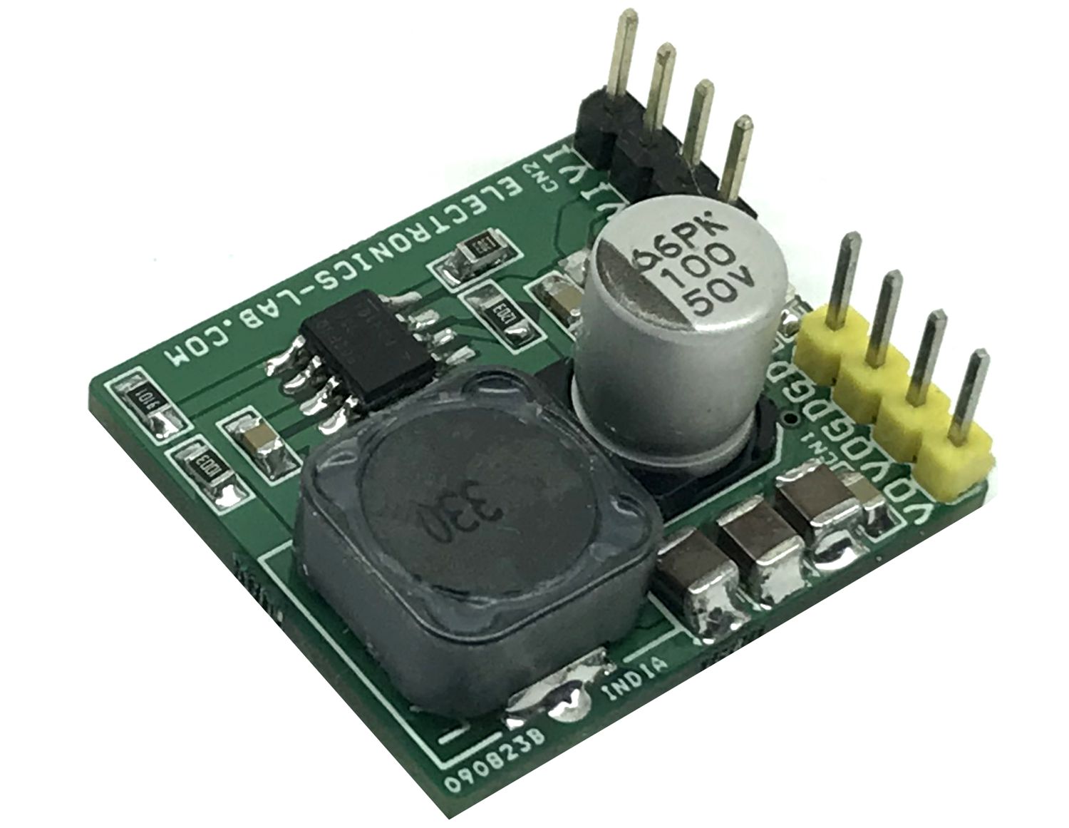
This DC/DC buck regulator project is based on LMR38020 chip that employs synchronous rectification to achieve high conversion efficiency on a small board. The project operates over a wide input voltage range of 14V to 48V to provide a regulated 12Vdc output at 400kHz switching frequency. The output voltage has better than 1.5% setpoint accuracy. Enable pin is connected to VIN using resistor R2. The device has built-in protection features such as cycle-by-cycle current limit, hiccup mode short-circuit protection, and thermal shutdown in case of excessive power dissipation.
Features
Tightly regulated output voltage of 12 V with 1.5% setpoint accuracy
Load Current 1Amp (Can provide Up to 2A), limited due to PCB thermal area.
Wide input voltage operating range of 14 V to 48 V
98% maximum duty cycle
Operating Frequency 400Khz
Force PWM operation to achieve low output voltage ripple, tight output voltage regulation at light load
The project provides 12V output with a maximum of 48V input. The input voltage is limited due to the input capacitor voltage rating. The input and output voltage can be changed with a few component adjustments. The IC has a wide input voltage range. The board can support a higher input power supply. Output also can be altered as per user requirements. Refer to the details below for various options. Also, refer to the datasheet of LMR38020 for more info.
The LMR38020 is protected from overcurrent conditions by cycle-by-cycle current limits on both the peak and valley of the inductor current. Hiccup mode is activated if a fault condition persists to prevent overheating. High-side MOSFET overcurrent protection is implemented by the nature of the peak current mode control. The high-side switch current is sensed when the high-side is turned on after a set blanking time. The high-side switch current is compared to the output of the error amplifier (EA) minus slope compensation every switching cycle. The peak current of high-side switch is limited by a clamped maximum peak current threshold, I high side LIMIT, which is constant. The current going through the low-side MOSFET is also sensed and monitored. When the low-side switch turns on, the inductor current begins to ramp down. The low-side switch is turned OFF at the end of a switching cycle if its current is above the low-side current limit, ILS_LIMIT. The low-side switch is kept on so that the inductor current keeps ramping down until the inductor current ramps below the ILS_LIMIT. Then the low-side switch is turned OFF and the high-side switch is turned on after a dead time.
Thermal Shutdown
The LMR38020 provides an internal thermal shutdown to protect the device when the junction temperature exceeds 163°C. Both high-side and low-side FETs stop switching in thermal shutdown. Once the die temperature falls below 150°C, the device reinitiates the power-up sequence controlled by the internal soft-start circuitry.
Soft Start
The integrated soft-start circuit prevents input inrush current impacting the LMR38020 and the input power supply. Soft start is achieved by slowly ramping up the target regulation voltage when the device is first enabled or powered up. The typical soft-start time is 4.0 ms.
The LMR38020 synchronous buck converter is designed to regulate over a wide input voltage range, minimizing the need for external surge suppression components. The LMR38020 operates during input voltage dips as low as 4.2 V, at nearly 100% duty cycle if needed, making it an excellent choice for wide input industrial applications and MHEV/EV systems.
The LMR38020 uses precision enable to provide flexibility by enabling a direct connection to the wide input voltage or precise control over device start-up and shutdown. The power-good flag, with built-in filtering and delay, offers a true indication of system status, eliminating the need for an external supervisor. The device incorporates a pseudorandom spread spectrum for minimal EMI and the switching frequency can be configured between 200 kHz and 2.2 MHz to avoid noise-sensitive frequency bands. In addition, the frequency can be selected for improved efficiency at low operating frequency or smaller solution size at high operating frequency.
Connection and Other Details
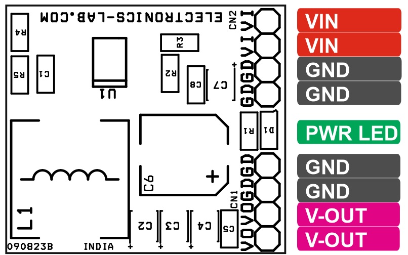
CN1 Pin 1,2 = Output Voltage, Pin 3,4 = GND
CN2 Pin 1,2 = +Input Power Supply 14 to 48V DC, Pin 3,4 = GND
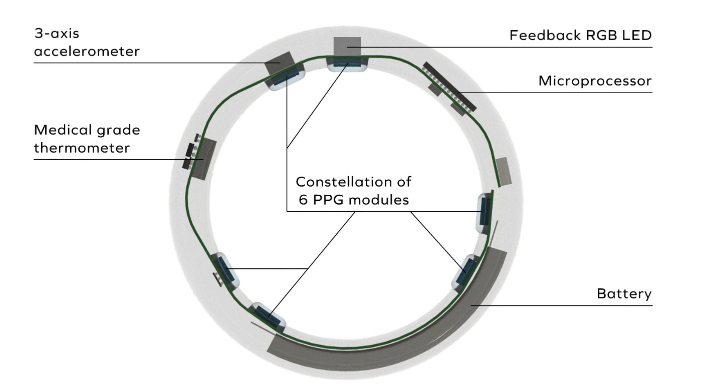
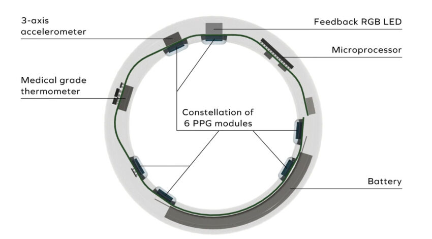
Two former EPLF Ph.D. students have created Iris, a smart ring the size of a wedding band that can monitor health like a high-end smartwatch. Marketed by Senbiosys, they have already raised five times more than the initial target of 100,000 francs.
In this time and age, everyone has heard about smartwatches and fitnesstrackers; these wrist-worn devices can do everything from telling time to monitoring your heart rate and making phone calls. Smartwatches and fitness trackers have been around for a while, but what is recently creating buzz around the internet is a smart ring. Smart Rings are wearable accessories that you put around your fingers. But most of the time, they are bulky and uncomfortable to wear.
That is where Senbiosys comes in; in collaboration with EPFL, they have developed a PPG sensor that concentrates all the monitoring capabilities of smartwatches into an area four times smaller, breaking all records. This breakthrough in miniaturization enables the device to need much less power than a smartwatch while achieving the same result.
A PPG sensor uses a light source like an LED and a photodetector to measure vital signs like heartrate, bloodoxygenlevels, breathingrate and bloodpressure, and more. The sensor does this by capturing the reflected light from the LED and feeding the information to an algorithm to calculate the vital signs. The YouTube video made by the founders explains the phenomenon a little better.
The PPG sensor developed by Senbiosys is just only four cubic millimeters in size, which is four times smaller than the ones found in smartwatches and fitness trackers. When developing micro semiconductors, miniaturization comes with the cost of power consumption. But extensive research at EPFL’s Integrated Circuits Laboratory in Neuchâtel has produced photodetectors that can pick up feeble signals just as clearly as a standard-sized sensor would do. This breakthrough in technology has made waves in the industry. Senbiosys co-founder says, “Our breakthrough has given rise to around 60 journalarticles in microelectronics and optical sensors,”. He says, “It’s also led to 11 patents, including some obtained at EPFL, and our work has been cited around 1,000 times.”
There are a couple of reasons why Iris came into existence, the most important one being wearing a smartwatchduringsleep is not only impractical but also uncomfortable. With Iris’s compact design and low power requirement, Iris looks like jewelry rather than a healthtracker. The ring contains 18 LEDs, and six photodetectors, which enables the device to measure health parameters accurately.
Senbiosys conducted their research at the Fribourg cantonal hospital to compare heart data. The research was performed to determine the accuracy and reliability of the miniaturizedsensors against traditionalsensors. After this, Boukhayma, one of the co-founders, said, “Our aim is not to make a tool for doctors but to help individuals track their health.” At the initial release, Iris can measure heart rate, step count, blood oxygen level, sleep quality, stress level, and calories burned. But with improvement and advancement in the algorithm, they can daa in more features to this device.
The company has raised 5 million francs and used that to develop some prototypes. In 2022, they decided to make a product for regular people called Iris. With crowdfunding, they plan to ship out Iris orders by late 2023 after sorting out the making process.
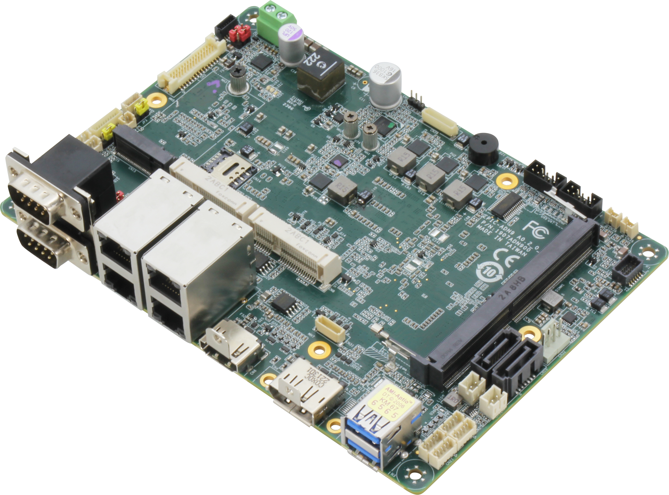
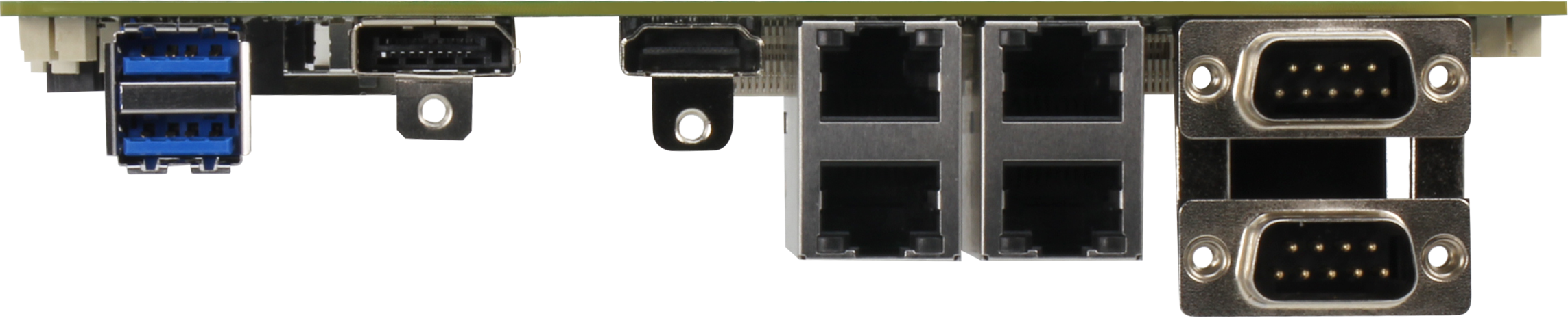
Supporting quadruple 2.5GbE LAN, three simultaneous displays, and efficient Intel® processors, the EPIC-ADN9 brings offers greater flexibility than ever before.
AAEON, a global leader in embedded computing, has introduced the EPIC-ADN9, featuring the newest iteration of Intel® technology on its 4.53″ x 6.50″ (115mm x 165mm) EPIC series of single-board computers.
Offering a range of embedded CPUs, including the Intel® Core™ i3-N305, Intel Atom® x7425E, Intel® Processor N50, and Intel® Processor N97, the EPIC-ADN9 strikes a balance between efficiency and performance. This selection of processors also provides support for Intel® UHD Graphics, enhancing the improved display interface configuration integrated by AAEON into the board. This configuration includes HDMI 1.4, DP 1.2, VGA, and 24/48-bit Dual-Channel LVDS.
Complementing the EPIC-ADN9’s display capabilities are up to four RJ-45 ports for Intel® I226-V Ethernet running at 2.5GbE, depending on the model. AAEON designed the board to be passively cooled, while also incorporating multiple options for image acquisition and high-resolution display. This design approach aligns with AAEON’s focus on applications such as entry-level gateway devices and digital signage.
Similar to previous generations of the EPIC board, the EPIC-ADN9 contains a wide 9V ~ 24V power input range, rendering it suitable for industrial deployment. Notably, the board hosts two physical serial ports for RS-232/422/485, in addition to four internal pin headers that support RS-232.
Coupled with its 16-bit GPIO and flexible storage options such as SATA III, full-size mPCIe, mSATA, and M.2 2242 B-Key slots, the EPIC-ADN9 demonstrates considerable potential in the realms of smart manufacturing and industrial automation, while retaining power-efficient operation.
The EPIC-ADN9 is now in mass production, with pricing and detailed information available through AAEON’s contact form.
For more information about the EPIC-ADN9, please visit its product page.
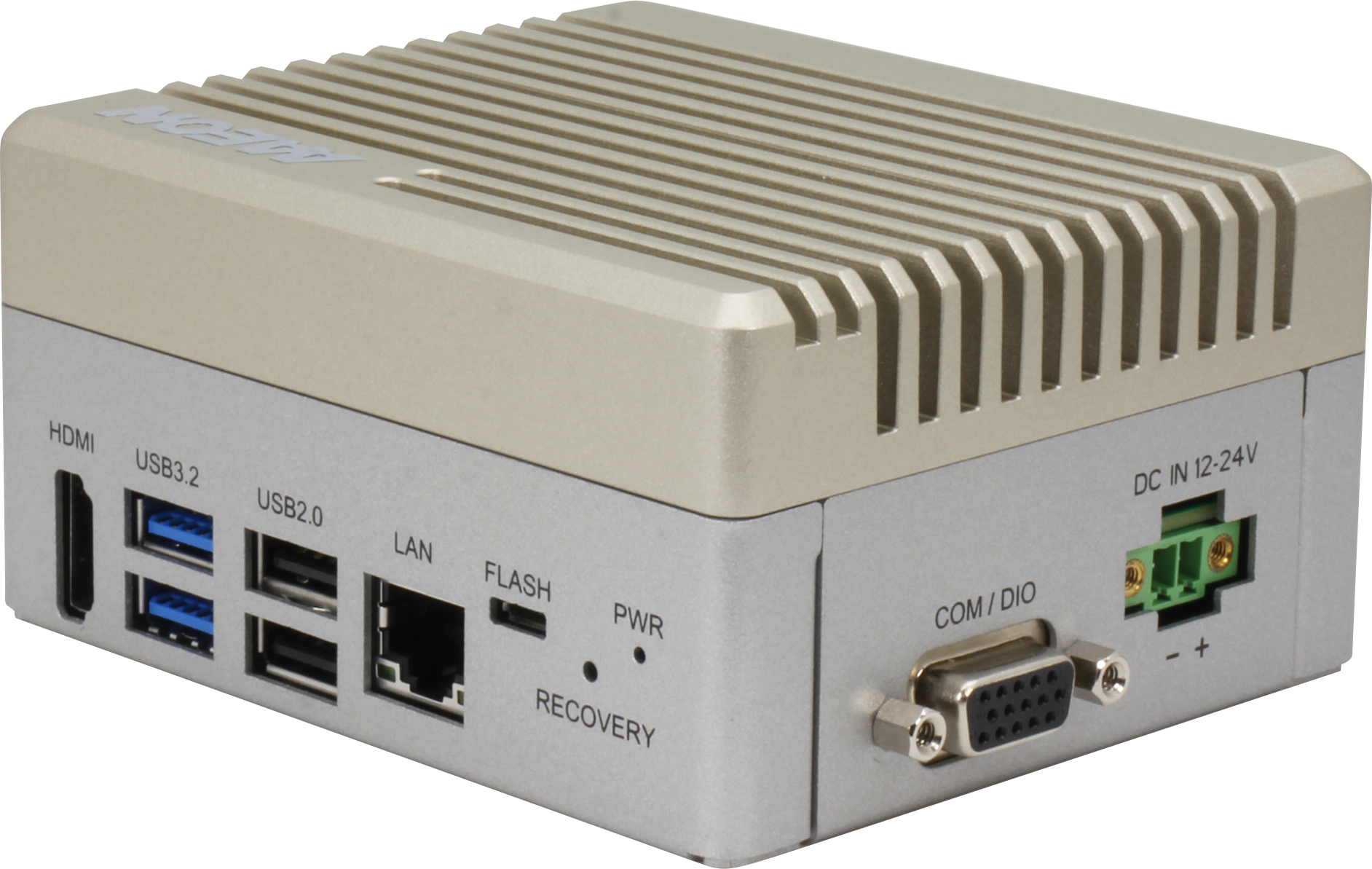
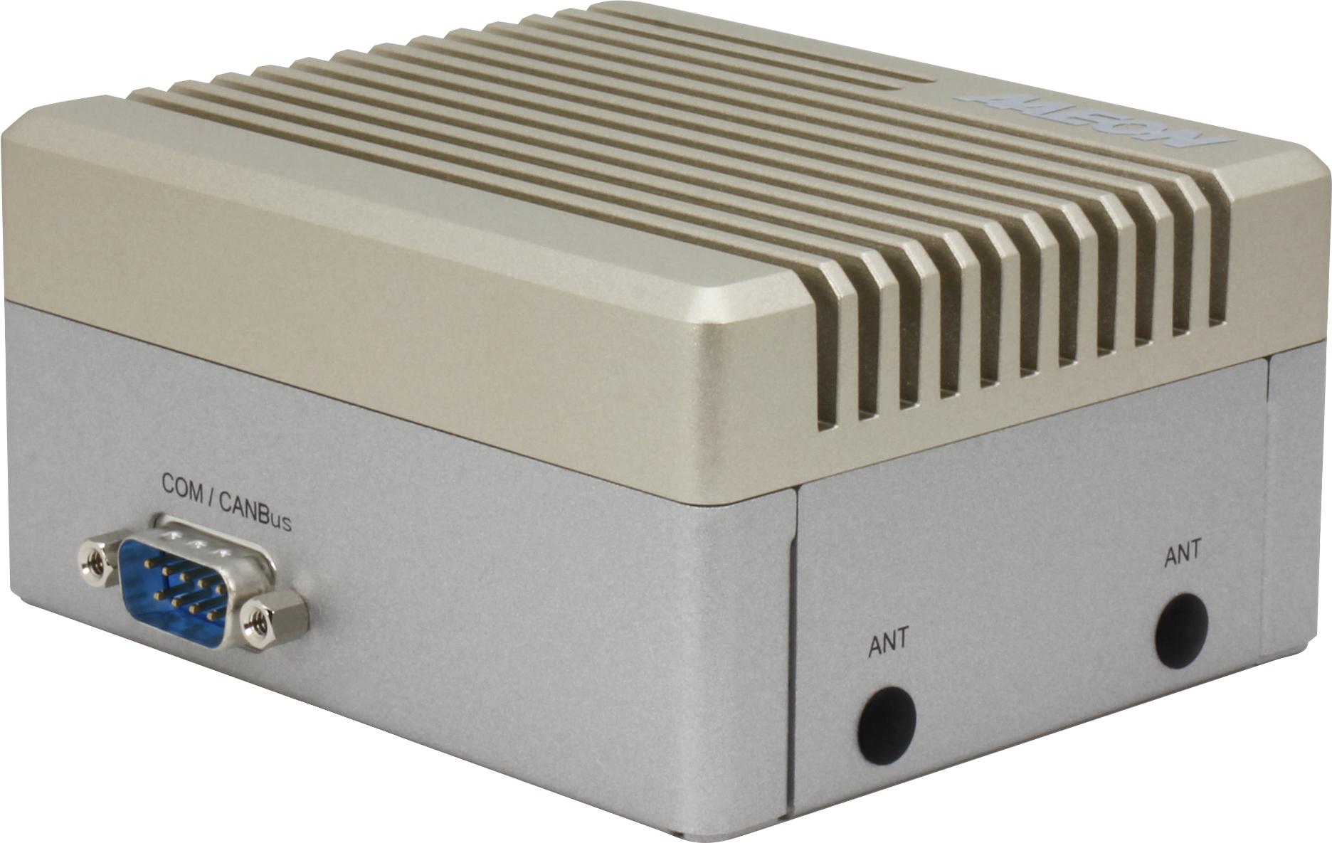
AAEON’s first AI system powered by the NVIDIA® Jetson Orin Nano™ combines the very best elements of edge computing with the type of versatility that’s only possible with expert engineering.
AAEON, a global leader in edge AI computing, has unveiled the BOXER-8621AI, its inaugural fanless embedded AI System powered by the NVIDIA® Jetson Orin Nano™ module. Geared towards applications such as AMR, fleet management, and traffic control solutions, the BOXER-8621AI seamlessly combines the NVIDIA Jetson Orin Nano’s impressive 20 TOPS of AI performance and NVIDIA Jetpack™ 5.0 SDK support with robust hardware, ensuring extended durability and longevity even in challenging environments. To bolster its resilience, the system boasts an operating temperature range of -15°C to 60°C, complemented by enhanced shock and vibration resistance.
The BOXER-8621AI is equipped with an array of interfaces tailored to its designated deployment domains. These include DB-9 and DB-15 ports for RS-232/422/485, CANBus, and GPIO, all backed by high-bandwidth LPDDR5 system memory. The system also incorporates four USB Type-A ports (two offering USB 3.2 Gen 2, and two offering USB 2.0), an RJ-45 port for gigabit LAN, and an HDMI 1.4 port for display output.
In terms of expansion capabilities, the system features an M.2 3042/3052 B-Key slot to accommodate 4G, 5G, as well as M.2 2242 B and M-Key storage modules. Additionally, it contains an M.2 2230 E-Key slot, granting Wi-Fi, Bluetooth, and additional storage as needed.
Designed for efficient space utilization, the system comes complete with a wall-mounting bracket, rendering it exceptionally suitable for constrained deployment spaces. Its compact chassis, measuring 4.13” x 3.54” x 2.05” (105mm x 90mm x 52mm), contributes to this.
“At AAEON, we continue to build on the opportunity that the NVIDIA Jetson Orin platform gives us to provide our customers with the newest and most innovative market-ready edge AI solutions,” Alex Hsueh, the Associate Vice President of AAEON’s Smart Platform Division said. “The BOXER-8621AI highlights our commitment to producing world-class products that incorporate modules from across the NVIDIA Jetson Orin range, with our roadmap firmly established to adopt the most advanced technology on offer and tailor our solutions to cater to different vertical markets,” Hsueh added.
The BOXER-8621AI is now available for order via both the AAEON eShop and its standard sales channels.
For more information about the BOXER-8621AI, please visit its product page.
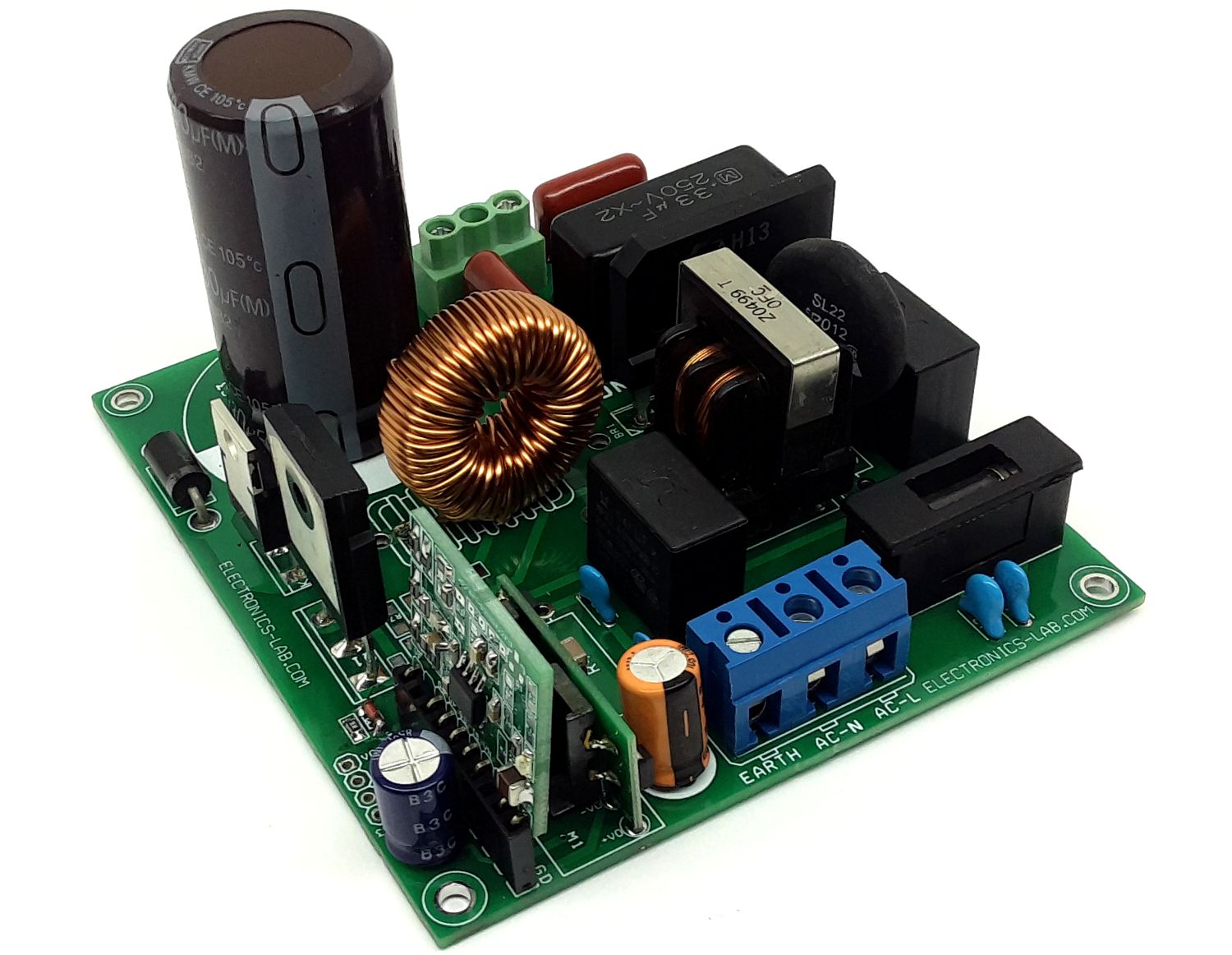
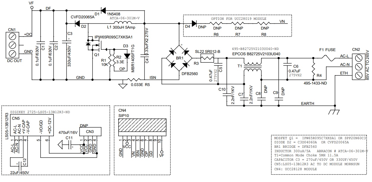
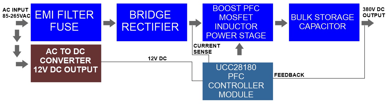
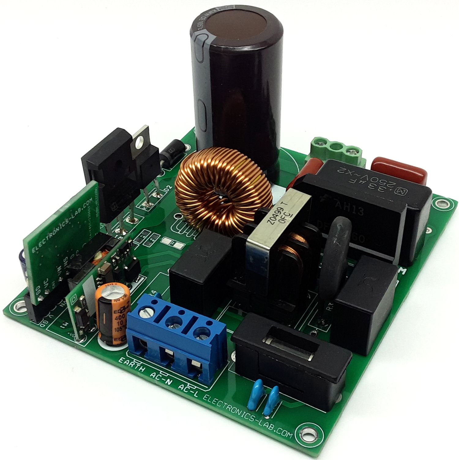
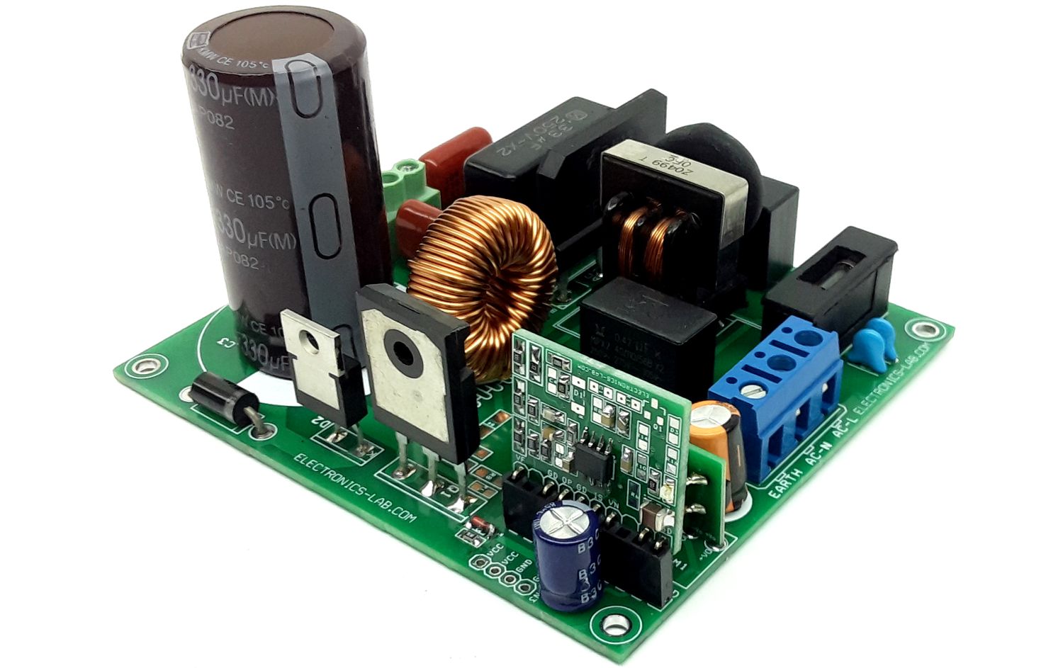
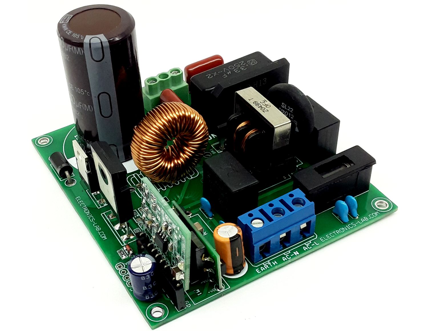
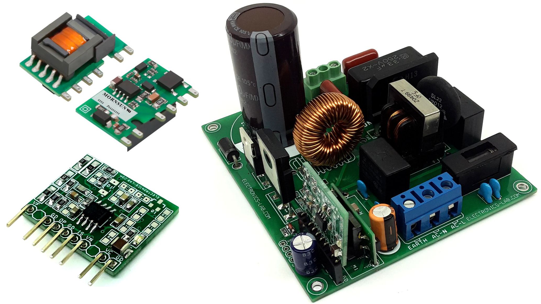
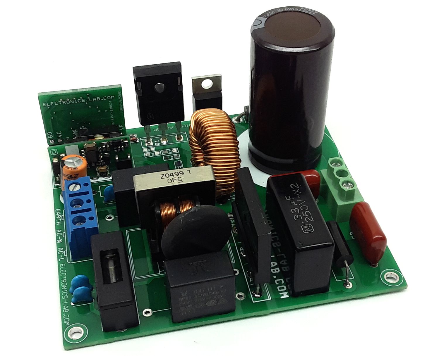
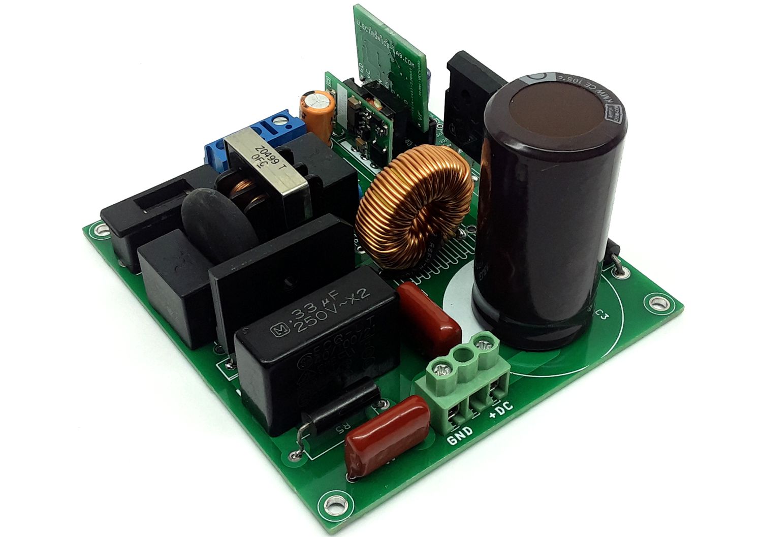
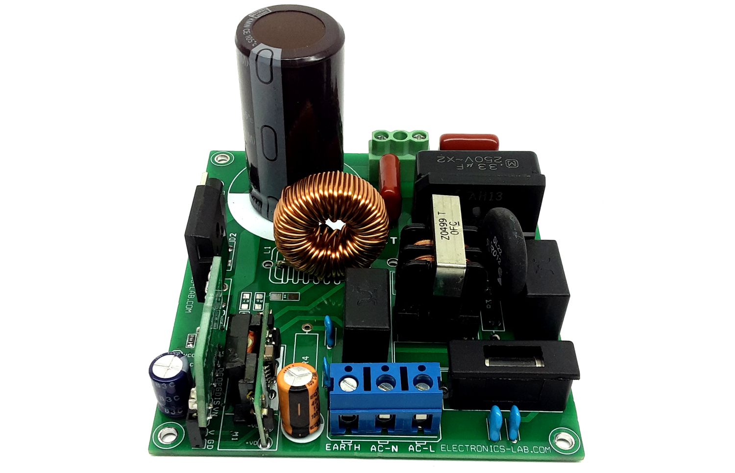
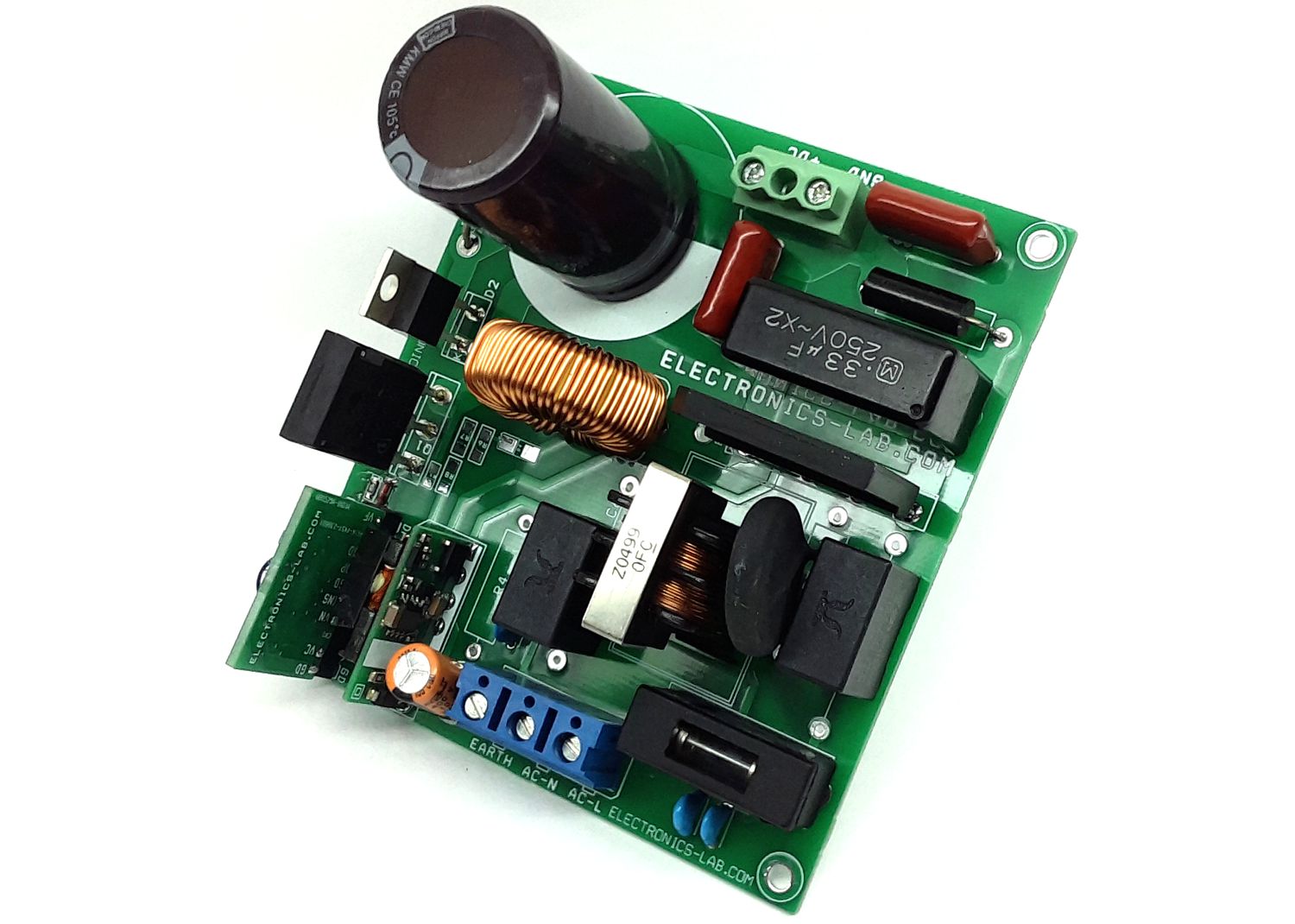
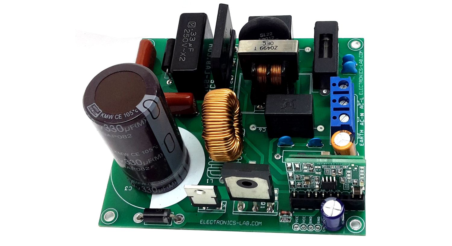
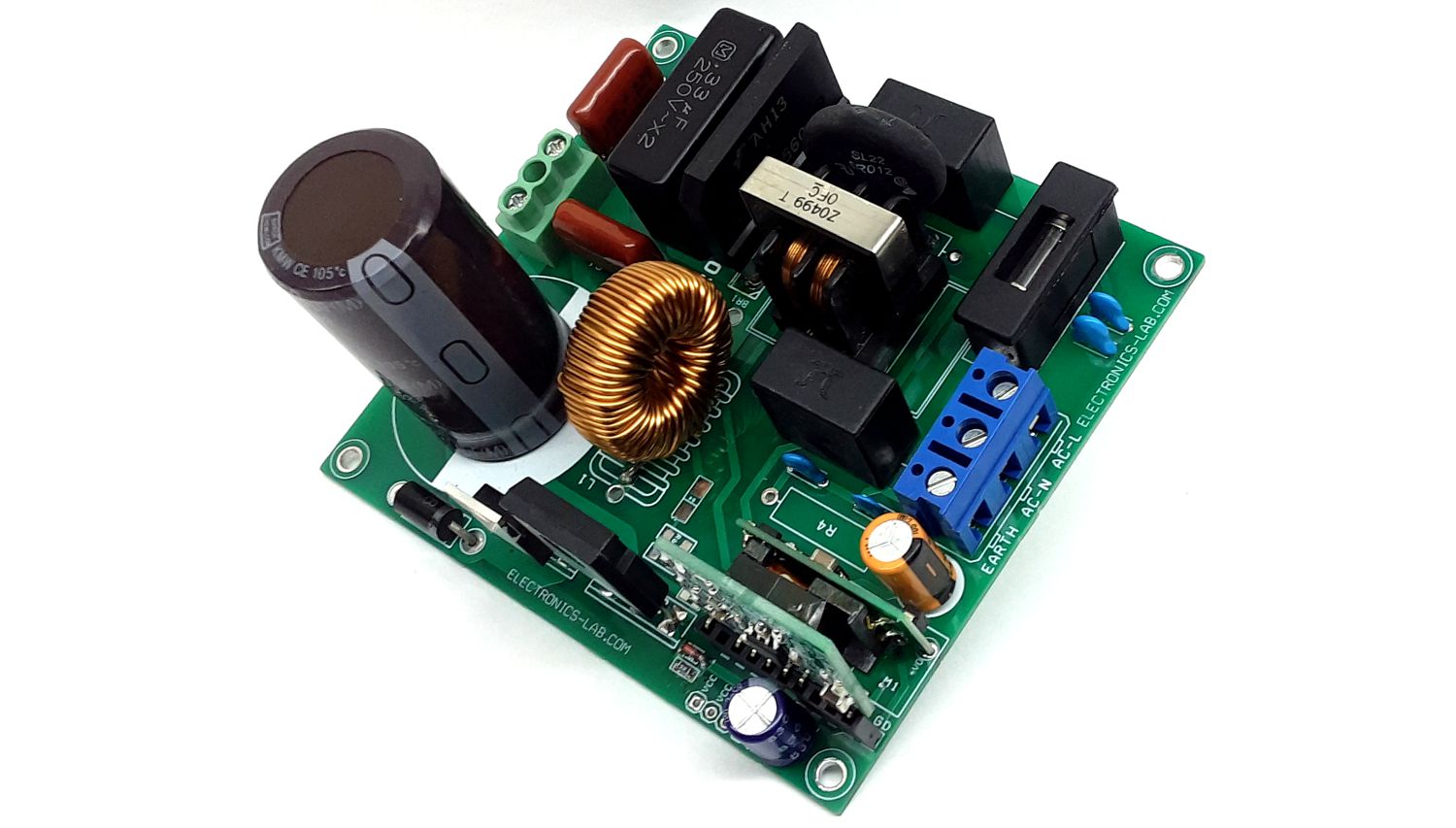
This 350W power factor boost converter is designed for inverter-fed BLDC/PMSM motor appliances, A/C units, Refrigerators, and industrial power supplies. The circuit is a continuous-conduction-mode boost converter implemented using a UCC28180 PFC controller module which provides all the necessary built-in protections. It’s a robust output supply protected for output cover current, output over-voltage, and output under voltage conditions. The converter has two parts, the main power board and the UCC28180 PFC controller/Breakout board. PFC boost converter provides 380VDC regulated output at 0.9A load current. The PFC converter accommodates an input voltage range of 85VAC to 265 VAC and uses average current mode control at a fixed programmable switching frequency of 120Khz.
If you use UCC28180 PFC controller module attached on downloads below, then you don’t need to place D4, R6, R7, R8.
If you use UCC28019 PFC controller module published on our website as a separate project, then you need to place D4, R6, R7, R8. Diode D4 = RS1MB-13-F, R6 = 1.8M 5% SMD SIZE 0805, R7 = 1.8M 5% SMD SIZE 0805, R8 = 0E SMD SIZE 0805. Diode D4 = can be 1KV 500mA-1A high speed switching diode
The board operates at lethal voltages and has bulk capacitors that store significant charges. Accidental contact can lead to lab equipment damage, personnel injury, and may be fatal. Please be exceptionally careful when probing and handling this board. Always observe normal laboratory precautions.
Features
Output 380V DC
Output Load Current 0.9A
Full Load Efficiency 94%
Input AC Range 85V to 265V AC
Input Frequency 47 to 63 Hz
No Load Input Current 70mA
Operating Frequency 120Khz
Average Current Mode PWM Control
No AC Line Sensing Needed
Soft Over Current and Cycle-by-Cycle Peak Current Limiting
VCC Under Voltage Lockout with Low Start-Up Current
Voltage Regulation Open Loop Detection
Output Over-Voltage Protection with Hysteresis Recovery
Soft Start
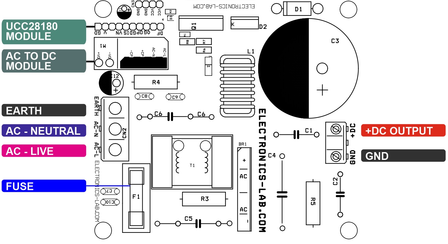
PCB Dimensions 97.79 x 89.22 mm
4 x 3mm Mounting Holes
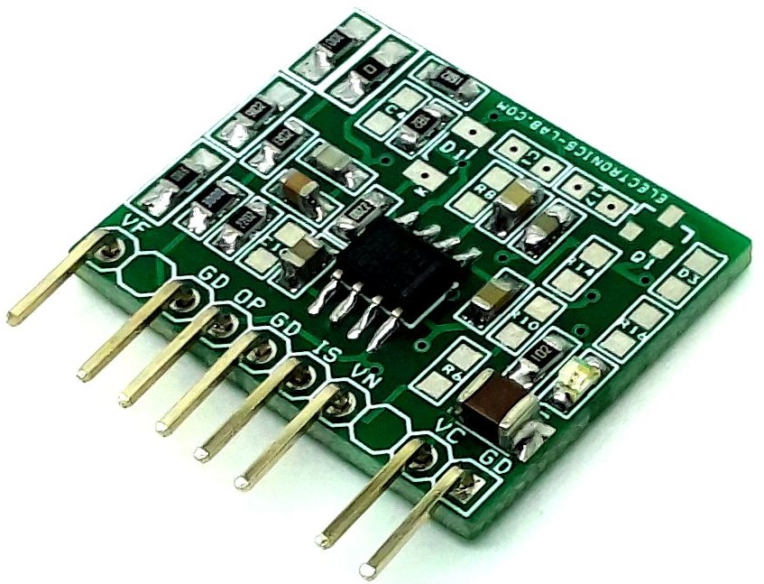
UCC28180 – PFC Controller (Schematic and PCB Layout in Downloads below)
The UCC28180 module provides high performance and offers a series of benefits to address the next-generation requirement of low THD standards for appliances. The UCC28180 is a high-performance, compact continuous conduction mode (CCM), Frequency is programmed 120Khz using R11 and R15 The UCC28180 uses trimmed current loop circuits to achieve less than a 5% THD from a medium-to-full load (50% to 100%). A reduced current sense threshold enables the UCC28180 device to utilize a 50% smaller shunt resistor, resulting in lower power dissipation while maintaining low THD. The UCC28180 also consists of an integrated fast gate driver, with a drive of +2-A source current and −1.5-A sink current, which eliminates the requirement for an external gate driver.
UCC28180 module
The UCC28180 device also has a complete set of system protection features that significantly improve reliability and further simplify the design.
Soft overcurrent
Cycle-by-cycle peak current limit
Output Overvoltage
VCC undervoltage lockout (UVLO) protection
Open pin protections (ISENSE and VSENSE pins)
Main Power Board
The main power board consists CN2 AC power input connector, Fuse F1 for short circuit protection, R4 Varistor for spike protection, EMI filter built using T1 choke, Capacitor C5, C6, C7, C8, C9, and C10. Resistor R3 NTC is provided to control the inrush current. BR1 bridge rectifier provides DC output from AC input. R5 is the current sense resistor, C4 acts as the filter capacitor, Q1 MOSFET acts as the switching transistor, and D2 high speed switching diode. C1, C2, and C3 are bulk storage capacitors. CN1 provides [email protected] output.
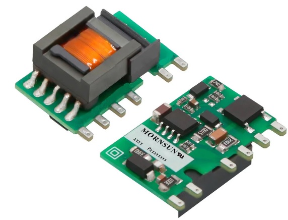
AC to DC Module (LS05-13B12R3)
This module provides 12V DC output from AC input. It is used to provide VCC power supply to UCC28180 PFC controller module/Breakout Board.