Comparing MEMS and Electret Condenser Microphones

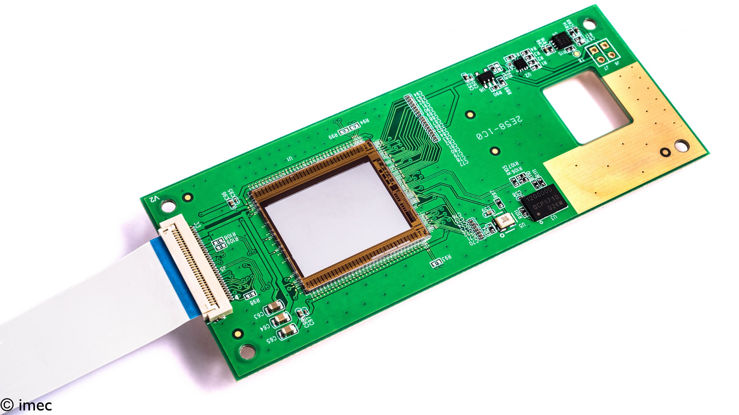
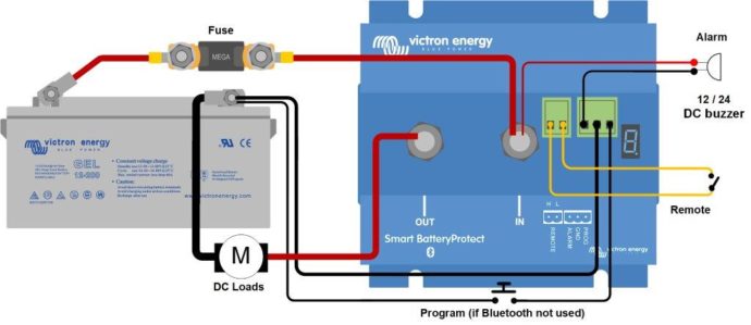
MEMS Microphone Basics

MEMS microphones are constructed with a MEMS (Micro-Electro-Mechanical System) component placed on a printed circuit board (PCB) and protected with a mechanical cover. A small hole is fabricated in the case to allow sound into the microphone and is either designated as top-ported if the hole is in the top cover or bottom-ported if the hole is in the PCB. The MEMS component is often designed with a mechanical diaphragm and mounting structure created on a semiconductor die.

Typical MEMS microphone construction

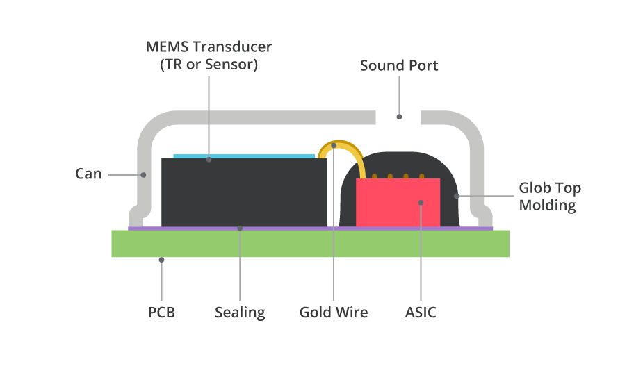
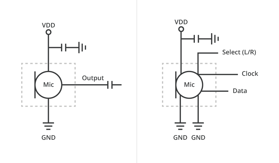
The MEMS diaphragm forms a capacitor and sound pressure waves cause movement of the diaphragm. MEMS microphones typically contain a second semiconductor die which functions as an audio preamplifier, converting the changing capacitance of the MEMS to an electrical signal. The output of the audio preamplifier is provided to the user if an analog output signal is desired. If a digital output signal is desired, then an analog-to-digital converter (ADC) is included on the same die as the audio preamplifier. A common format used for the digital encoding in MEMS microphones is pulse density modulation (PDM), which allows for communication with only a clock and a single data line. Decoding of the digital signal at the receiver is simplified due to the single bit encoding of the data.

Left: analog MEMS microphone application schematic Right: digital MEMS microphone application schematic

Electret Condenser Microphone Basics

Electret Condenser Microphones (ECM) are constructed as shown in the figure below.

Typical electret condenser microphone construction

An electret diaphragm (material with a fixed surface charge) is spaced close to a conductive plate, and similar to MEMS microphones, a capacitor is formed with the air gap as the dielectric. Voltage across the capacitor varies as the value of the capacitance changes due to sound pressure waves moving the electret diaphragm, ΔV = Q/ ΔC. The capacitor voltage variations are amplified and buffered by a JFET internal to the microphone housing. The JFET is typically configured in a common-source configuration, while an external load resistor and dc blocking capacitor are used in the external application circuit.

By Bruce Rose, Principal Applications Engineer, CUI @ www.cui.com

…read more

Raman-on-a-chip boosts High-Resolution Handheld Spectroscopy

Next week, at SPIE BIOS and SPIE Photonics West 2019 in San Francisco, imec, a world-leading research and innovation hub in nanoelectronics and digital technologies, presents an on-chip solution for Raman spectroscopy – based on a newly patented concept – providing high optical throughput and high spectral resolution. The solution could pave the way for affordable high-end handheld Raman spectroscopy device opening up many new applications. Imec invites technology partners and IDMs to further develop the technology into a commercial application.

Raman spectroscopy is a powerful technique, most often used to determine chemical and material composition. Application areas include the medical, food, even space industries. Because of the inherent nature of the technique, existing devices are rather bulky (tabletop) and have a price range of a few hundred thousand dollars/euros. Handheld solutions exist, but for the moment fail to reach the desired performance for high-end applications, largely because of the limited scaling capacity of conventional dispersive Raman spectrometry whereby scattered light is focused on a slit. Scaling while maintaining high spectral resolution (< 1nm) means reducing the size of the slit which immediately limits the optical throughput.

Thanks to a new concept, for which a patent is pending, imec has now been able to overcome this performance barrier. By massive parallelization of waveguide interferometers integrated monolithically on top of a CMOS image sensor, both high optical throughput and high spectral resolution can be reached in a miniaturized device. This novel system is built in imec’s SiN biophotonics platform which guarantees robustness and compatibility with high-volume manufacturing. Part of the work was performed under the EU-funded IoSense program.

Pol Van Dorpe, principal member of the technical staff at imec:

“We are very pleased to have achieved this milestone which can mean a breakthrough for the general applicability of Raman spectroscopy. One could even think about smartphone integration. With the right partners we see many application opportunities in areas like food analysis, melanoma detection, or skin hydration. In the medical domain, we see opportunities for in-line measurements during surgery or endoscopy. And for space exploration, the ability to perform material analysis with a compact system is of tremendous value.”

www.imec-int.com

4A PWM Controlled Unipolar Stepper Motor Driver using STK672-740

The project published here is a high-performance Unipolar stepper motor driver that offers PWM controlled high current output. An Arduino board and the project published here can be combined to create a good Unipolar stepper motor driver with micro-stepping, supply 36v DC and load current up to 4A. This board requires a sequence of 4 phase pulses which can be feed and generated using Arduino or any other microcontrollers.  IC incorporates various functions like built in over current detection, over heat output OFF, fault output (active low) when over current or over heat detected, and also has built in power on reset. LED D2 is the power indicator, LED D1 indicates a fault. PR1 trimmer potentiometer provided to set the current. Refer to datasheet of STK672-740 for pulse sequence and timing information. The projects supports 5 Wire, 6 Wire and 8 Wire Stepper Motors in unipolar mode.

The board works perfectly with motor supply up to 36V DC, however motor power supply is possible to go up to 50V DC, in this case remove LM317 regulator, and supply 5V from external power supply.

Features

  • Motor Supply 36V DC ( Up to 50V DC Possible Read Note)
  • Logic Supply 5V DC ( On Board LM317 Regulator Provides 5V)
  • Motor Load Up to 4Amps
  • Required large size heat sink for IC
  • Built-in overcurrent detection function, overheat detection function ( output current OFF)
  • Fault signal ( active low) is output when over current or overheat is detected
  • Built-in power on reset function
  • Phase signal input driver activated with an active low and incorporates a simulation ON prevention function
  • Supports Schmitt input 2.5V high level input
  • Incorporating a current detection resistor, motor current can be set using trimmer pot
  • Enable pin can be used to cut output current while maintaining the excitation mode.
  • PCB Dimensions 30.32MM x 44.04MM

Schematic

Parts List

Block Diagram

Input Signals

Interface

Connections

Photos

STK672-740 Datasheet

Vamrs Releases Toybrick RK3399Pro SBC & cheaper $69 RK3399 based Rock960 SBC

Vamrs has launched their “Toybrick RK3399Pro” SBC that runs Linux or Android on the AI-enabled RK3399Pro. A cheaper Model C version of its RK3399 based Rock960 SBC is also released. 96rocks, Vamr’s community site announced that the TB-RK3399Pro is currently available only from Rockchip in Fuzhou, China, but Vamrs is willing to ship a small number of oversea orders. The company also developed Rockchip’s official dev board for the RK3399 SoC, named the Rockchip RK3399 Sapphire. The RK3399Pro is the same as the original, with 2x Cortex-A72, 4x -A53, and a Mali-T860 GPU. The difference is an addition of an up to 3.0-TOPS performing Neural Network Processing Unit (NPU), which supports Tensorflow, Tensorflow Lite, Caffe, and other deep learning systems.

Toybrick RK3399Pro Board

The Toybrick teaser page lists a 3GB RAM, 16GB eMMC version and a 6GB/32GB version, which are “under $299.” The SBC is equipped with a microSD slot, an Ethernet port (presumably GbE), plus a WiFi module. It also includes a USB 3.0 host and Type-C ports as well as dual USB 2.0 ports and a micro-USB debug port. The Toybrick RK3399Pro is fitted with DP 1.2 and HDMI 2.1 ports, and also MIPI-DSI and eDP display interfaces. According to Vamrs, the SBC enables dual MIPI-CSI connections driven by the RK3399Pro’s “dual ISP with pixel processing capability of up to 1300W pixels. Available also is an 8-channel digital microphone array input, a speaker interface, and a headphone jack.

The RK3399Pro is also fitted with RS232 and fan interfaces, and also a reset button, plus 4x PCIe lanes and a mini-PCIe slot. The SBC runs dual-boot, with pre-installed Android and Linux with one-button OS switching. Their product page promises to start shipping this month in limited quantities, with the price is yet to be settled, but at least one version is projected to sell for under $299. The Model C, which sells for $69 offers only 1GB of RAM and offers an empty eMMC socket instead of 16GB or 32GB, plus the pre-existing microSD slot.

Varms Rock960 model C

For the RAM, it offers the faster LPDDR4 instead of the LPDDR3 on the earlier models. The 1GB of RAM  could be insufficient for exploiting the functionality of the RK3399. The Model C has switched to a USB 2.0 Type-C without DP, from the USB 3.0 Type C port with DP support, leaving only the HDMI 2.0 port. It utilizes a lower-cost version of the dual-band 802.11ac module without 2×2 MIMO. The new module clocks at 200Mbps instead of 867Mbps. The Model C board offers an M.2 (4x PCIe 2.1) slot that enables an optional M2 Extend board for NVMe SSD. Available also  is MIPI-DSI and CSI, a USB 2.0 host port, 40- and 60-pin expansion connectors and a wide-range 8-18V input. The $69 1GB version is available by Seeed, but a product table speculates the Model C may soon be available in 2GB ($79) and 4GB ($99) models.

The Toybrick RK3399Pro SBC is available for pre-orders starting at under $299 in limited amount, and shipping to begin as early as this month. More information can be found in Vamrs’ TB-RK3399Pro announcement. The Model C is available at Seeed for $69 with 1GB RAM.

Weller WT 1014 Affordable Soldering Station

1-Channel Soldering Station Set, digital 95 W with soldering iron WSP 80 Robust.

  • Power unit WT 1, 1 channel with soldering iron WSP 80 Robust and safety rest WSR 201
  • WSP 80 Robust soldering iron (80 W) with power response tips for all standard applications, robust version. Tip family LT
  • OFF time, Process window, Lock function, Offset

Technical data

  • Dimensions W x D x H (mm): 149 x 138 x 101
  • Channels: 1
  • Voltage: 230 V, 50/60 Hz
  • Heating output: 95 W
  • Display: Backlit LCD
  • Temperature range: Adjustable from 50°C – 550°C (150°F – 950°C), Adjustable temperature range varies among tools
  • Temperature stability °C: ±2
  • Temperature accuracy °F: ±17
  • Temperature stability °F: ±4
  • Dimensions W x D x H (inch): 5.87 x 5.43 x 3.98
  • Temperature range (depends on tool) °C: 50 – 550
  • Temperature range (depends on tool) °F: 150 – 950
  • Weight (ca) in kg: 1.9
  • Equipotential balance
  • Fuse: 0,5 A
  • WT compatible
  • ESD-safe

Introduction Video

This soldering station is reviewed on Elektor and Weller WT 1014 is available at ~€350 from various distributors online.

Torex launches positive voltage LDO regulators based on CMOS

The XD6506 is a series of voltage regulators from Torex Semiconductor that is manufactured using CMOS processes. The positive voltage LDO regulators are qualified to AEC-Q100 Grade 2. The regulators achieve low supply current, 0.8 microA (typical) and consist of a reference voltage source, an error amplifier, a current fold-back circuit, and a phase compensation circuit plus a driver transistor.

The output voltage is selectable in 0.1V increments within a range of 1.2 to 5.0V using laser trimming technologies. The XD6506 series is also compatible with low ESR ceramic capacitors for output stability. The current limiter’s fold-back circuit also operates as a short protect for the output current limiter and the output pin.

The CE function allows the output of the regulator to be turned off to reduce power consumption. The regulators are environmentally-friendly and comply with the EU RoHS Directive and are lead-free.

Torex Semiconductor provides CMOS power management ICs targeted at battery powered and energy efficient applications. Torex specialises in CMOS analogue technology, with LDO voltage regulators, voltage detectors and DC/DC converters making up the core product offering.

Application Circuit

http://www.torexsemi.com

Texas Instruments LMZ1420x SIMPLE SWITCHER® Power Modules for High Output Voltage

Texas Instruments LMZ1420x Series SIMPLE SWITCHER® Power Modules for High Output Voltage feature an integrated shielded inductor, simple PCB layout, and a flexible startup sequencing using external soft-start and precision enable. These power modules offer protection against inrush currents and input UVLO and output short circuit protection. Their high efficiency reduces system heat generation and they have low package thermal resistance. The LMZ1420x Series power modules each come with a single exposed pad and standard pinout for easy mounting and manufacturing.

Features

  • Integrated shielded inductor
  • Simple PCB layout
  • Flexible startup sequencing using external soft-start and precision enable
  • Protection against inrush currents
  • Input UVLO and output short circuit protection
  • -40°C to 125°C junction temperature range
  • Single exposed pad and standard pinout for easy mounting and manufacturing
  • Low output voltage ripple
  • Pin-to-pin compatible family
  • Fully enabled for Webench® Power Designer

Specifications

  • Input voltage range: 6V to 42V
  • Output voltage: as low as 5V
  • Efficiency: up to 97%

Block Diagram

more information: www.ti.com

Samsung Breaks Terabyte Threshold for Smartphone Storage with eUFS

Powered by the company’s fifth-generation V-NAND, the new Universal Flash Storage offers 20x more storage than a 64GB internal memory and 10x the speed of a typical microSD card for data-intensive applications.

Samsung Electronics, the world leader in advanced memory technology, today announced that it has begun mass producing the industry’s first one-terabyte (TB) embedded Universal Flash Storage (eUFS) 2.1, for use in next-generation mobile applications. Just four years after introducing the first UFS solution, the 128-gigabyte (GB) eUFS, Samsung has passed the much-anticipated terabyte threshold in smartphone storage. Smartphone enthusiasts will soon be able to enjoy storage capacity comparable to a premium notebook PC, without having to pair their phones with additional memory cards.

The 1TB eUFS is expected to play a critical role in bringing a more notebook-like user experience to the next generation of mobile devices,” said Cheol Choi, executive vice president of Memory Sales & Marketing at Samsung Electronics. “What’s more, Samsung is committed to assuring the most reliable supply chain and adequate production quantities to support the timely launches of upcoming flagship smartphones in accelerating growth of the global mobile market.

Within the same package size (11.5mm x 13.0mm), the 1TB eUFS solution doubles the capacity of the previous 512GB version by combining 16 stacked layers of Samsung’s most advanced 512-gigabit (Gb) V-NAND flash memory and a newly developed proprietary controller. Smartphone users will now be able to store 260 10-minute videos in 4K UHD (3840×2160) format, whereas the 64GB eUFS widely used in many current high-end smartphones is capable of storing 13 videos of the same size.

The 1TB eUFS also possesses exceptional speed, allowing users to transfer large amounts of multimedia content in significantly reduced time. At up to 1,000 megabytes per second (MB/s), the new eUFS features approximately twice the sequential read speed of a typical 2.5-inch SATA solid state drive (SSD). This means that 5GB-sized full HD videos can be offloaded to an NVMe SSD in as fast as five seconds, which is 10 times the speed of a typical microSD card. Furthermore, the random read speed has increased by up to 38 percent over the 512GB version, clocking in at up to 58,000 IOPS. Random writes are 500 times faster than a high-performance microSD card (100 IOPS), coming in at up to 50,000 IOPS. The random speeds allow for high-speed continuous shooting at 960 frames per second and will enable smartphone users to take full advantage of the multi-camera capabilities in today and tomorrow’s flagship models.

Samsung plans to expand the production of its fifth-generation 512Gb V-NAND at its Pyeongtaek plant in Korea throughout the first half of 2019 to fully address the anticipated strong demand for the 1TB eUFS from mobile device manufacturers around the world.

BatteryProtect makes your Battery Smart

Prevent your battery from charging non-essential loads with BatteryProtect.

BatteryProtect is one of those smaller but much sought after products, one that is shipped in the many thousands. The latest version now has Victron ‘Smart’ tech. No more fiddling with wires to program, as the new Smart BatteryProtect uses VictronConnect over Bluetooth to simplify and reduce setup time. Smart BatteryProtect is used to disconnect a battery from non-essential loads before it is completely discharged (which would damage the battery) or before it has insufficient power left to crank an engine for example.

Product Range

Voltage and current ratings to suit the majority of applications:

  • 12-24V 65A
  • 12-24V 100A
  • 12-24V 220A
  • 48V 100A
Connection Diagram

Key features

  • Easy programming/setup using VictronConnect.
  • Often used in lithium systems due to low standby current in comparison to a relay.
  • Lithium system remotely controllable disconnect switch.
  • Ideal for vehicles, solar installations, boats and motorhomes.
  • Solid state switching for ignition proof safety and longevity.
  • Lower energy consumption than closing a relay.

Mobile APP

VictronConnect App Screenshoot


more information: www.victronenergy.com

TOP PCB Companies