Economical Siglent SDS5000X 350MHz-1GHz Oscilloscopes

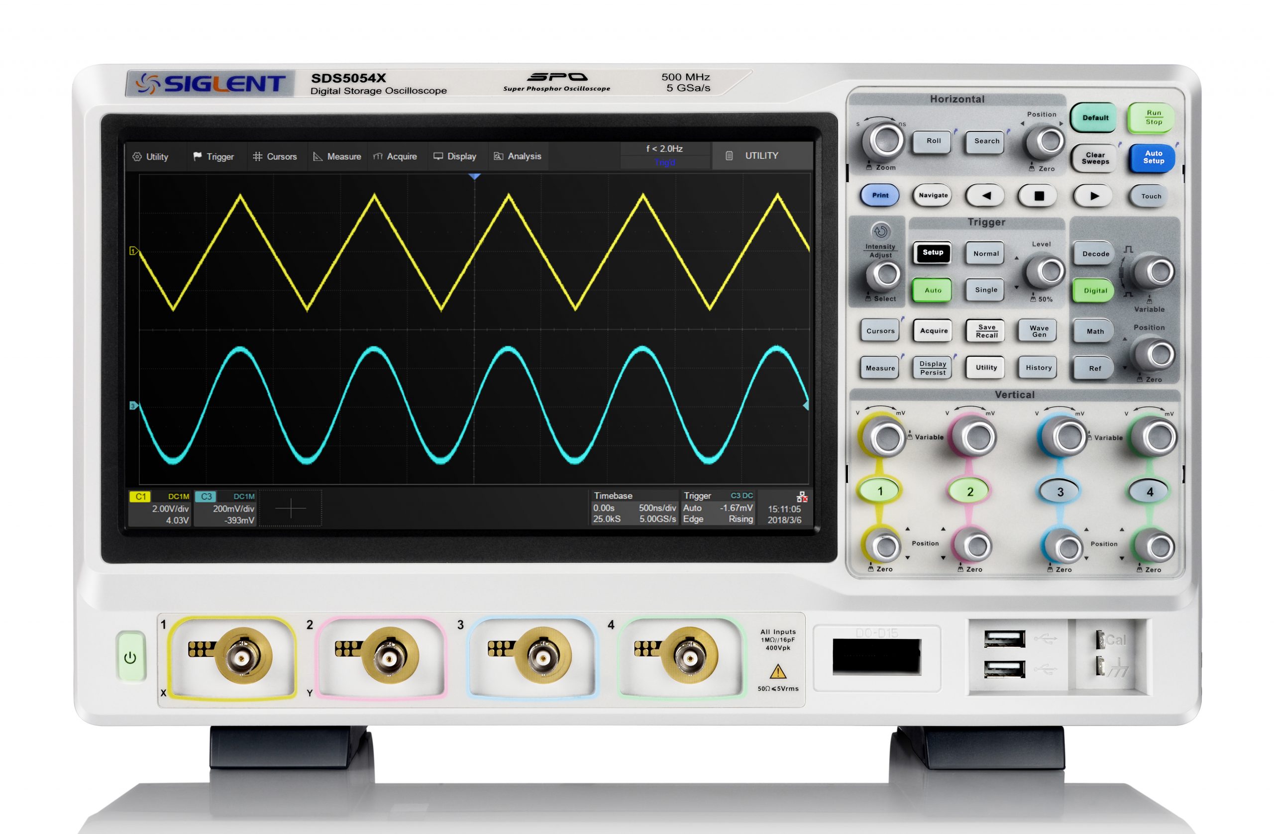
Sampling at 5GSa/s with a standard record length of 250Mpts/channel, this series includes the first 1GHz oscilloscope made by Siglent.  The SDS5000X’s impressive waveform capture rate is up to 480,000 frames/sec with multiple powerful triggering modes.

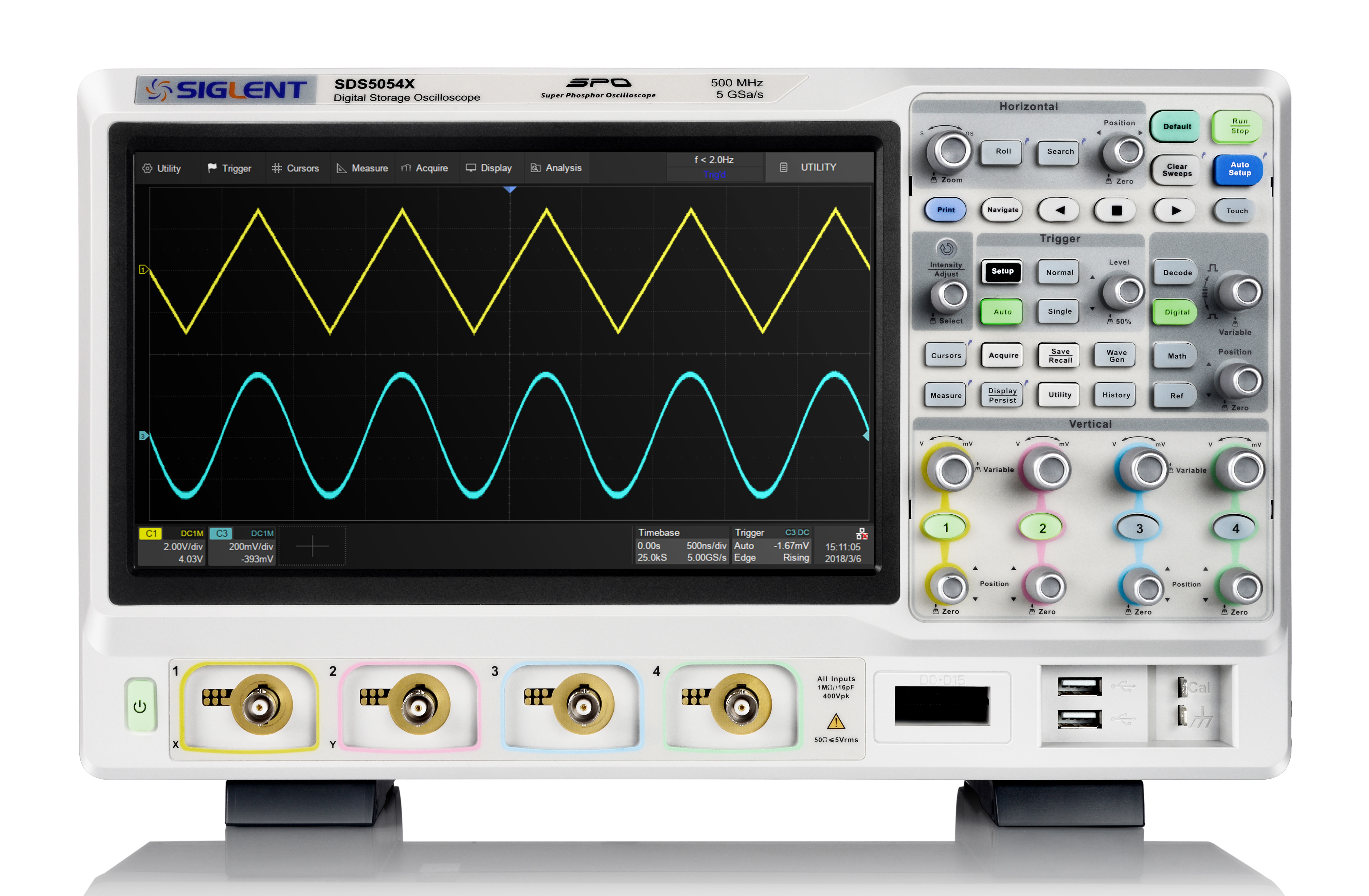
Saelig Co. Inc. announces the new economical, high performance Siglent SDS5000X series of advanced digital storage oscilloscopes, which are available in 2 or 4 channel versions with bandwidths of 350MHz, 500MHz, and 1GHz – Siglent’s highest yet.  With a maximum sample rate of 5GSa/s, these premium scopes offer a maximum record length of 250Mpts to allow for deep memory investigation of glitches and infrequent events, and they also have the option of 16 digital channels for true mixed signal analysis. The SDS5000X series has a maximum waveform capture rate of up to 480,000wfm/s in Sequence Mode.  Visibility of waveforms is enhanced by a 256-level intensity-grading display function with a helpful color temperature display mode. The large 10.1’’ capacitive touch screen supports highly efficient multi-touch gestures, and a user-friendly single button feature for many commonly used functions.  This greatly enhances the operational ease of the SDS5000X series of instruments. An external mouse and keyboard can also be connected to add to their navigation and notation capabilities.

The SDS5000X’s innovative digital trigger system offers high sensitivity and low jitter, with multiple powerful trigger modes that include serial bus decode triggering, as well as edge, slope, pulse, window, runt, interval, dropout, pattern, qualified and video (HDTV supported). History waveform recording, Sequence acquisition, Search and Navigate functions all combine to allow extended waveform records to be captured, stored, and analyzed.

SDS5000X instruments are designed with an impressive array of measurement and math capabilities as well as extensive serial decoding of protocols such as I2C, SPI, UART, CAN, LIN, CAN FD, FlexRay, I2S and MIL-STD-1553B.   The low background noise design supports a minimum setting of 0.5mV/div.  A Digital Voltmeter is also included in the design for a visible indication of measured data.

To add digital debug capabilities, there is an MSO option which adds 16 digital channels with maximum waveform capture rate up to 1.25GSa/s and a record length up to 62.5Mpts. An external 25MHz function/arbitrary waveform generator with built-in multiple predefined waveforms offers a useful signal source for test purposes.

Multiple interfaces are provided: USB Host, USB Device (USBTMC), LAN (VXI-11, Telnet, socket, web), Pass/Fail, Trigger Out, 10 MHz In, 10 MHz Out, and VGA output.  Remote control is also supported via SCPI commands, or by using a web browser to access the built-in web server via the LAN port.

These oscilloscopes are made by Siglent Technologies, a leading high quality test equipment manufacturers, with a growing worldwide reputation.

The Siglent SDS5000X series start at $2,899 and are available on www.saelig.com in US.

TEA5767 – FM Receiver Module

Based on the chip of the Philips TEA5767, this tiny module allows to realize, with the addition of very few external components, a stereo FM radio with reception frequency from 87.6 MHz to 108 MHz .. Used in MP3 players, MP4, mobile phones, etc.

The single-chip TEA5767/68 is a miniature, digitally tuned radio IC that utilizes an entirely new radio architecture concept that replaces passive components and complex circuitry, with on-board silicon, drastically reducing the overall bill of materials and making design-in easier. It requires zero external alignments, resulting in shorter design times and lower manufacturing costs due to simplified component placement and reduced logistics overhead. Also, being adjustment free, it delivers increased quality and reliability, both in manufacture and throughout its lifetime in your end application. As well as offering increased functionality in handheld devices, the radio IC is ideal for integration in a wide range of applications, where its minimal interaction with the rest of your application helps avoid reception / transmission interference. The TEA5767/68 also features very low power consumption and its small footprint makes it ideal for applications where board space is at a premium. Capable of tuning to European, US and Japanese FM bands, the TEA5767/68 does not need an external FM discriminator and handles IF selectivity entirely on-chip.

Features

  • High Sensitivity due to integrated low noise input amplifier
  • FM Mixer for conversion to IF
  • RF AGC (Automatic Gain Control) circuit
  • Standby Mode
  • Soft Mute
  • Autonomous search turning function
  • Adjustment free stereo decoder
  • Phase Locked Loop synthesizer turning system
  • Internal FM IF selectivity
  • LC Tuner Oscillator with low cost fixed chip inductors
  • Fully integrated FM demodulator
  • Crystal reference frequency oscillator

Specifications

  • Typical Operating Voltage : 3V
  • Operating Voltage Range : 2.5V ~ 5V
  • Frequency Range : 76MHz ~ 108MHz
  • Interface : I2C
  • Dimensions: 11.2 x 11 mm

Resources

The TEA5767 module costs ~$3 from various distributors online.

LTM4638 – 20 VIN, 15 A and 12 A Step-Down DC-to-DC μModule® Regulators

The LTM4638 is a complete 15A step-down switching mode µModule (power module) regulator in a tiny 6.25mm × 6.25mm × 5.02mm BGA package. Included in the package are the switching controller, power FETs, inductor and support components. Operating over an input voltage range of 3.1V to 20V, the LTM4638 supports an output voltage range of 0.6V to 5.5V, set by a single external resistor. Its high efficiency design delivers up to 15A continuous output current. Only bulk input and output capacitors are needed.

The LTM4638 supports selectable discontinuous mode operation and output voltage tracking for supply rail sequencing. Its high switching frequency and current mode control enable a very fast transient response to line and load changes without sacrificing stability.

Fault protection features include overvoltage, overcurrent and overtemperature protection.

Features

  • Complete Solution in <1cm2 (Single-Sided PCB) or 0.5cm2 (Dual-Sided PCB)
  • 6.25mm × 6.25mm × 5.02mm BGA Package
  • Wide Input Voltage Range: 3.1V to 20V
  • 0.6V to 5.5V Output Voltage
  • 15A DC Output Current
  • ±1.5% Maximum Total DC Output Voltage Error Over Line, Load and Temperature
  • Differential Remote Sensing Amp
  • Current Mode Control, Fast Transient Response
  • External Frequency Synchronization
  • Multiphase Parallel Current Sharing with Multiple LTM4638s
  • Output Voltage Tracking
  • Selectable Discontinuous Mode
  • Power Good Indicator
  • Overvoltage, Overcurrent and Overtemperature Protection

Introducing the LTM4626 and LTM4638, µModules®

This brief animated video highlights the new 4th Generation LTM4626 and LTM4638. These small packaged µModules® have inductors for heat sinks and are highly power-efficient.

LD20 Liquid Flow Sensor Is Part of Wearable Drug Delivery IoT Platform

At this year’s MD&M West trade fair (Anaheim, United States), the sensor expert Sensirion and Quantex Arc Ltd will be presenting an innovative concept study in the field of infusion technology – Quantex’s new wearable drug delivery IoT Platform “Quantex 4C”.

Sensirion is a leading manufacturer of environmental as well as gas and liquid flow sensors. The cost-effective LD20 single-use liquid flow sensor, which has been used for this concept study, is exceptionally compact and measures flow rates in the micro and milliliter per hour range with outstanding precision and reliability thanks to the patented CMOSens® Technology. Additionally, it features sensitive failure detection mechanisms to help counteract, for example, occlusions and air-in-line. Quantex is an innovative leader in single-use disposable pump technology. The pump’s design is based on a rotary, fixed displacement principle thus is much less sensitive to variables such as line pressure, fluid viscosity and flow rate.

The new wearable drug delivery IoT platform “Quantex 4C” demonstrates an innovative approach to infusion therapies. It integrates connectivity with a modular drug delivery platform and enables continuous monitoring of the therapy with the help of a single use liquid flow sensor for safe ambulatory treatments.

Real time bidirectional flow verification at the low flow rates that are typical for the targeted application and the sensor’s compact form factor made the Sensirion LD20 single-use liquid flow sensor the ideal choice”, said Paul Pankhurst, Founder and CEO of Quantex.

The objective of the presented study is to demonstrate the possibilities of a comprehensive drug delivery system to the medical technology industry. The compactness, low power consumption and cost-effectiveness of both, sensor and pump, allow the design of a wearable device which controls and monitors the drug delivery therapy simultaneously. Such a connected drug delivery platform opens up entirely new possibilities for all involved stakeholders. While patients and clinicians benefit from an increased ease of use and confidence in the therapy, low maintenance and less training efforts; it allows healthcare and pharma companies to capture vital adherence data and simplifies patient compliance.

Disposable LD20 Flow Sensor by Sensirion

Reliable failure detection is a central requirement for next generation drug delivery devices. Ambulatory treatments and wearable applications will only be successful if patients as well as clinicians trust the reliability of those next generation devices.

Visit both companies, Sensirion (Booth 1556) and Quantex (Booth 1958), from February 5 – 7, 2019 at MD&M West in Anaheim to learn more about the concept study.

You can see the smart drug delivery platform first-hand and test it using a demonstrator at Quantex’s booth.

More information is available at: www.sensirion.com/LD20 and www.quantex-arc.com

PSLab is an Open Source Platform For STEM Education

I remember many years ago, when I was trying to acquire data with hardware especially with “Data Acquisition” devices, I was gifted a device that I must say reshaped my life – It was the NI myDAQ. The NI myDAQ was a product from National Instrument, and it allowed students to perform hands-on experimentation in or outside the lab. It was like your personal lab arsenal in your pocket, and you could turn it to most instruments you can think off.

NI myDAQ impacted the STEM Education, but those are the days of NI myDAQ. A new entry to this arena is the PSLab also called Pocket Science Lab, which I am personally impressed about and the NI myDAQ is not really a competitor of it in terms of cost, features, openness, welcomes, and many more. PSLab is an complete open source platform for STEM Education.

PSLab Device
PSLab Open Source Device For STEM Education

Pocket Science Lab is a small open source device that provides an array of test and measurement instruments for doing science and engineering experiments by merely plugging it into a PC or an Android Phone via a USB port. The device can act as a voltmeter for measuring voltage, a personal oscilloscope, logic analyzer, a programmable voltage and current source, a lux meter, and even as a signal generator. Open Source Android or desktop apps can be used to view and collect the data. FOSSASIA and OpnTec develop PSLab in collaboration with a global community of Open Source developers.

Although, PSLab isn’t to replace professional equipment, it is more tailored for teaching STEM and still can be used by anyone from students, teachers, makers, scientists, to engineers.

PSLan android app
PSLab Android App for Measurement and Testing

PSLab is not limited and can be further extended from the default features. It can be easily extended with various types of sensors and modules. You can directly connect an ESP8266 and turn the device to an IoT based Lab Kit or plug in hundreds of compatible I2C standard sensors to the PSLab pin slots, and they usually work without any need for extra programming. Moreover, the device is fully opensource. The Android app source code is available on Github, the Python desktop app source code, the schematics, PCB layout, and Gerber files are available on Github as well, the PIC24 MCU firmware in another repository in Github.

Below are the device specifications:

  • MCU – Microchip PIC24EP256GP204 16-bit microcontroller @ up to 70 MHz with 32KB SRAM, 256KB flash
  • Wireless Connectivity
    • Footprint for ESP8266 module (ESP-12E) for 802.11 b/g/n WiFi (on bottom of board)
    • Bluetooth extension slot
  • 4-Channel, up to 2MSPS Oscilloscope
  • 12-bit Voltmeter. Programmable gain. Input ranges from +/-10mV to +/-16V
  • 3x 12-bit Programmable voltage sources: +/-3.3V,+/-5V,0-3V
  • 12-bit Programmable current source. 0 – 3.3mA
  • Supports Advanced Plugins/Add-on Modules
  • 4-Channel, 4MHz, 15nS Logic Analyzer
  • 2x sine/triangular wave generators. 5Hz to 5KHz. Manual amplitude control
  • 4x PWM generators. 15nS resolution. Up to 8MHz
  • Capacitance Measurement. pF to uF range
  • 8x I2C, SPI, UART data buses for an accelerator, gyroscope, humidity sensor, etc.…
  • ICSP Programmer – PICkit3 compatible programmer slot
  • Dimensions – 101 x 53 x 13 mm
  • Weight – 30 grams
PSLab with python app
PSLab being using the python desktop app.

The vision of PSLab is to miniaturize laboratories and make scientific instruments accessible for everyone. The device is available for purchase from various vendors at about $64.90 on Seed Studio, EUR 59.00 on Pslab.io store, and some other stores. More information about the product is available on the product page.

Infineon Gallium Nitride Power Devices

Infineon adds GaN (Gallium Nitride) to its power portfolio: CoolGaN™ and GaN EiceDRIVER™ ICs.

The next essential step towards an energy-efficient world lies in the use of new materials and technologies. Wide bandgap semiconductors enable greater power efficiency, smaller size, lighter weight, lower cost, or all together.

Infineon is uniquely positioned in the power semiconductor market, mastering all power technologies from silicon (Si) like CoolMOS™ SJ MOSFETs and IGBTs to wide bandgap materials like silicon carbide (SiC) and gallium nitride (GaN). Its CoolGaN™ devices will significantly enhance designer’s ability to deliver the compact, high performance power systems of the future.

Discover Infineon’s newly launched portfolio of CoolGaN™ switches in SMD packages. Perfectly combinable with parts of the dedicated, single-channel, functional and reinforced isolated GaN EiceDRIVER™ IC family. Enter a new era of efficiency with Infineon.

Benefits

  • Perfect choice for high frequency and high power density applications
  • GaN EiceDRIVER™ ICs for excellent robustness and efficiency
  • High quality volume supply that enables faster time-to-market
  • Reduced BOM costs and overall system cost

more information

CoolGaN™ 600 V e-mode HEMTs

With CoolGaN™, Infineon launches a GaN enhancement mode high electron mobility transistor (e-mode HEMT) portfolio with industry-leading field performance enabling rugged and reliable systems at an attractive overall system cost.

The e-mode concept is a single-chip solution and hence facilitates further integration either on the chip or package level. Infineon brought its enhancement mode concept to the maturity, required for demanding applications, delivering at the same time the highest performance among all available GaN HEMTs. GaN switch performance features low charge and excellent dynamic performance in reverse conduction compared to silicon FET options.

Infineon’s CoolGaN™ 600 V impresses with highest PFC efficiency (>99.3% for 2.5 kW PFC) and highest density for same efficiency (>160 W/in³ for 3.6 kW LLC with >98% efficiency). The CoolGaN™ portfolio is built around high performing bottom- and top-side cooling SMD packages supporting high frequency operations. Lower parasitics and good thermal performance guarantee to fully exploit the benefits of GaN.

Target applications

  • Servers
  • Hyperscale datacenters
  • Telecom
  • Wireless charging
  • Chargers
  • Adapters
  • SMPS

GaN EiceDriver™ IC family

Drive high voltage gallium nitride (GaN) HEMTs with the most robust and efficient single-channel isolated GaN EiceDRIVER™ ICs on the market.

Infineon’s newly launched GoolGaN™ switches portfolio is easy-to-use thanks to a perfectly matching gate driver IC portfolio. By introducing the GaN EiceDRIVER™ IC family, Infineon extends its range of one-channel galvanically-isolated gate driver ICs.

The new components with high gate current for fast turn-on and robust gate-drive topology have been developed to optimize the performance of enhancement mode GaN HEMTs with non-isolated gate (diode input characteristic) and low threshold voltage. Resulting, driver complexity has been significantly reduced (medium effort for design-in) as no more customized drivers are needed.

Target applications

  • High-voltage bridgeless totem-pole PFC stages and high-voltage resonant LLC stages in telecom and server SMPS
  • Active-clamping flybacks in AC adapters
  • Three-phase motor drivers
  • Class E wireless charging
  • Class D audio amplifiers

powered by OEMsecrets.com

ADSM302 – Andonstar 1080P Digital Microscope for repair work

Digital microscope with 1080p resolution and integrated 5″ display, HDMI/AV/USB/microSD interface

ADSM302 is a multifunctional digital microscope individually designed, developed and manufactured by Shenzhen Andonstar Technology Co. It supports Full HD, high object distance, multifunction, multi-output at the same time. With help of the Andonstar measuring software, it can easily meet many different requirements in many industries, such as industrial overhaul and teaching demonstration.

Product description

  • Screen size 5 inch
  • Image sensor 3 Mega Pixels HD Sensor
  • Video output 1080P Full HD (via HDMI) ;720P (via PC)
  • Video format real time play via HDMI w/o recording; MJPEG recording via PC Software
  • Magnification Up to 560 times (HDMI monitor 22 inch)
  • Photo resolution 12M
  • Photo format JPEG
  • Focus range 5cm to 22cm
  • Frame rate Max 30f/s under 600 Lus Brightness
  • Video-output interfaceHDMI/AV
  • Storage Micro-SD card, up to 32G
  • Power source 5V DC
  • Light source2 LED with the stand

Review Video

Sample Photos

ADSM302 is available for purchase online for ~$280 from various distributors.

Wi-Fi Stepper motor Controller

Control over Wifi and enable IoT interface for any stepper motor all the way up to 85V and 10A rms.

Wi-Fi Stepper is a feature-packed, easy-to-use, stepper motor controller accessible over Wi-Fi. It can handle small to big stepper motors under high current. You can send crypto-secured commands over Wi-Fi from a computer, phone, or any other platform. Integration with other controllers is possible using the step clock and direction input pins. Wi-Fi Stepper makes controlling a stepper motor easy and productive.

Applications

  • Home automation
  • Robotics
  • CNC routers
  • Security access devices
  • Pumps and dispensers

Big or small, bring your motor into the IoT world.

Many projects need a way to interact with the real world. For a lot of applications, stepper motors are the preferred way. They work well at slow to medium speeds and without gearbox reductions. There are plenty of inexpensive NEMA mounts to choose from. They have excellent torque ratings and can even provide high torque at extremely low speed. Stepper motors can run at speed, or as a servo that holds position at any angle. Stepper motors are commonly used in CNC applications and are a great entry-level motor to learn the basics.

With a proper power supply, this project supports most motors on the market. With its voltage and current ratings, even the mammoth NEMA 42 is within its comfort zone for the most demanding applications.

(1) NEMA 11 (2) NEMA 17 (3) NEMA 23 (4) NEMA 34 (5) NEMA 34 high torque

Servo Control Software

Drag and edit servo position quickly and intuitively or enter in precise angles. View openloop position feedback and manage step sizes.

Quickstart guide servo mode control pane

Features & Specifications

  • Motor Compatibility
    • Stepper driver: powerSTEP01
    • NEMA preset profiles: 11, 17, 23, 34, 42
    • Maximum speed: 4500 RPM
    • Operating modes: both current (charge pump) and voltage (PWM)
    • Boards chainable for simultaneous multiple motor control
  • Configuration Options
    • Current control down to 1/16 microstepping with high hold torque
    • Voltage control down to 1/128 microstepping and smooth motion with low noise
    • Safety features (current/voltage/thermal shutdowns)
    • Advanced speed profiles (acceleration and deceleration slopes)
    • Waveform generation and timing settings
    • Power supply sag/swell compensation
    • Predictive current compensation
    • Back EMF adjustment
    • Stall detection
  • Power
    • Voltage regulation: MAX15062 high-efficiency voltage regulator
    • Input voltage: 9-85 V
    • Maximum output current: 10 A
  • Wi-Fi
    • Chipset: ESP8266 Wi-Fi chip in an ESP-WROOM-02 module
    • Security: ATECC508A crypto-authentication module – for generating access keys and verifying commands from authorized clients
  • Hardware Interfaces
    • External step-clock
    • I2C
    • SPI
    • UART
    • GPIO
    • ADC
  • Software
  • Physical Dimensions
    • Weight: 1.25 oz (35 g)
    • Board size: 3” x 2.25” (76 mm x 63.5 mm)

The project is live on www.crowdsupply.com and has 25 days left.

PB50 Detects Radiation between 1 and 5.2 microns

LASER COMPONENTS is a world leading manufacturer of lead salt infrared detectors. From our research and production facility in Arizona we supply customers all over the world with these industrial grade thermal detectors.

These detectors work on the principle that photons incident on the polycrystalline thin film promote electrons across the bandgap increasing the conductivity of the material in turn decreasing the resistance of the substance. The polycrystalline lead selenide (PbSe) units detect radiation in the wavelength range between 1 and 5.2 microns.

The resistance of photoconductive detectors depends on the incident light. PbSe has a particularly strong inner photoelectric effect: When infrared light reaches the lead selenide detector, the resistance is reduced. The detectors can be used uncooled at a wavelength of up to 4.7 µm. At room temperature, they exhibit a detectivity D* of greater than 1010. At low temperatures, they achieve an even higher performance level; in addition, the wavelength shifts to 5.2 µm.

The devices are manufactured in standard TO style packages and have long expected lifetimes making them ideal for fit and forget applications such as gas sensing, surface inspection and flame detection. The PB50 device is a collection of TE cooled polycrystalline biased single element PbSe detectors that operate at room temperature with a 20% cut off at 4.9 microns and a maximum element size of 6 x 6 mm2.

LCDGP

Application Fields

PbSe detectors react very quickly and are thus particularly well suited for high-speed applications, such as, for example, the detection of hot spots. They are also used in medical gas analysis (CO2 measurements), emissions measurements in the industrial field and the automobile industry, and in the measurement of moisture and hydrocarbons.

more information: www.lasercomponents.com

ON Semi – Silicon Photomultiplier RB-Series

ON Semi’s RB Series of red-enhanced second generation Silicon Photomultipliers (SiPM) with high responsivity at a low bias voltage.

MicroRB−Series sensors are the second release of Silicon Photo− multipliers (SiPM) from ON Semiconductor’s R-Series range. These sensors provide further sensitivity improvements in the red and NIR region of the electromagnetic spectrum. All R-Series SiPM sensors feature high responsivity, fast signal response and a low temperature coefficient of operating voltage, all achieved at a low bias voltage.

The sensor is packaged in a compact and robust MLP (molded lead frame) package that is suitable for reflow solder processes. Both the sensor and the package are designed for volume production with the product delivered on tape and reel.

SiPM sensors are an improvement over avalanche photodiodes (APD) and PIN diodes due to their high gain and single photon sensitivity. This enables the detection of low reflectivity targets at very long distance in LiDAR applications. Unlike the similarly-operated SPAD that can only detect single photons, the SiPM overcomes this limitation by incorporating a ‘microcell’ structure that allows for multi-photon detection with a high dynamic range.

It is strongly recommended that those new to SiPM sensors consult the Introduction to Silicon Photomultipliers application note.

Features

  • High gain and detection efficiency
  • From a unique ‘fast output’ terminal
  • PDE of >10 % at 905 nm
  • Single photon sensitivity
  • 1 mm sensor size, which a choice of microcell size
  • Compact and robust MLP package
  • <50 V bias voltage

Applications

  • 3D ranging & sensing
  • Medical imaging
  • Hazard & threat
  • Biophotonics & sciences
  • High energy physics

more information: www.onsemi.com

TOP PCB Companies