Weller soldering station for less than 150€

New soldering station WE1010 proves that even a very decent station can be available at an affordable price. It´s primarily designed for schools, students, demanding hobbyists, developers etc.

Having a reliable Weller station without paying more than 150 Euro (excl. VAT) sounds quite good, doesn´t it?

It´s true that a decent soldering station from less famous brands can be bought for even less than 100 Euro, however, usually we´ll find some aspect which the given soldering station doesn’t meet – ergonomics, (non-intuitive) operation, reliability, ESD safety, portfolio of tips, serviceability, availability of spare parts,…

New WE line (efficiency line) meets all the above mentioned, including ESD safety, which is not that common in this price level.

As could be expected, Weller didn’t go for compromises and also the WE1010 station is designed to withstand demanding professional usage. However, in respect to overall concept, it´s preferentially intended for schools, students, demanding hobbyists, developers etc.

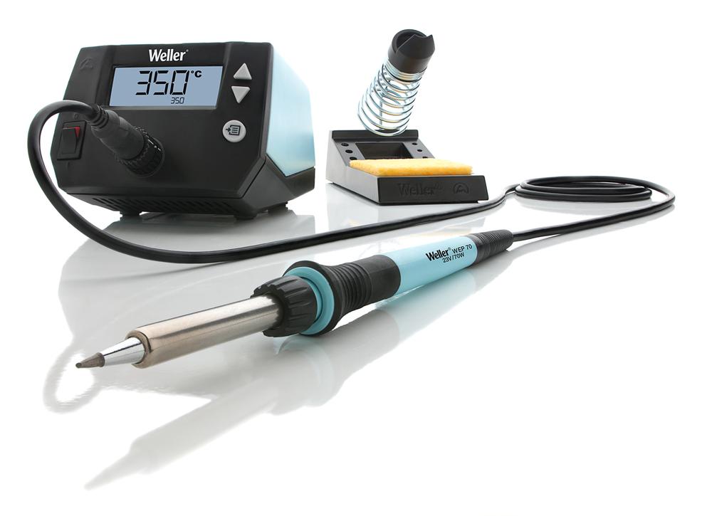
WE1010 has an LCD display and intuitive navigation by means of a menu button. By its consecutive pressing it´s possible to activate or adjust these functions:

  • standby time
  • offset (from -40 to +40°C)
  • choice of units °C/ °F
  • password lock/ unlock.

By a combination of buttons it´s also possible to set back the station into factory settings. New ergonomic WEP70 soldering tool has increased power to 70W and uses classic well-proven and cost-effective tips of the ET series (choice of 23 types). Also a tool cord is highly flexible with a heat-resistant silicone insulation. New PH70 stand (safety rest) is of a well-proven design with a high stability.

Modules offer both Wi-Fi and dual-mode Bluetooth at the same time

u-blox announces multiradio and gateway modules with concurrent Wi-Fi and dual-mode Bluetooth connectivity. The NINA‑W15 module series offers much design versatility, built‑in security, and proven software support.

Thalwil, Switzerland – October 24, 2018 u‑blox (SIX:UBXN), a global provider of leading positioning and wireless communication technologies, has announced the NINA‑W15 multi-radio and gateway module series, which can simultaneously support both Wi‑Fi 802.11 b/g/n connections and dual‑mode Bluetooth connectivity. This includes support for both Bluetooth low energy and Bluetooth BR/EDR. Concurrent support for these radio interfaces delivers much design versatility. The modules will be particularly useful in products such as gateways and hubs that need to connect local Bluetooth and/or Wi‑Fi peripherals to a wider‑area network.

The NINA‑W15 modules offer the ideal combination of radio interfaces, security features, proven connectivity software, and a small footprint necessary to enable cost‑effective industrial and medical applications

says Stefan Berggren, Senior Product Marketing Manager, Product Center Short Range Radio at u‑blox. “Several industries are focusing on digitalization and a common scenario is to connect a huge number of sensors and actuators to a back‑end system or to cloud service, for analysis and visualization or even controlling applications,” he adds.

Key applications for the modules include industrial automation, such as machine control, industrial terminal and remote controls, building automation, and smart building/home equipment such as HVAC and lighting control. Other potential use cases include retail point‑of‑sale terminals, telematics control units, and medical equipment such as defibrillators and urology monitors.

The NINA‑W15 modules will help IoT device developers to secure their designs by supporting features such as secure boot, Wi‑Fi enterprise security, end to end security, Bluetooth secure connections, and secure simple pairing. The modules are also supplied with pre‑flashed u‑blox connectivity software. This has been proven in the market for 15 years, and supports several connectivity use cases, such as multiple individually controlled connections, simultaneous GATT protocol and Serial Port Service, and simultaneous peripheral and central role. These features can be accessed by a host microcontroller by using simple AT commands to configure and control the modules, and to control communications with external Bluetooth and Wi‑Fi devices.

The modules are compact and available with an internal antenna (NINA‑W152, measuring 10 x 14 x 3.8 mm) or a pin through which to drive an external antenna (NINA‑W151, measuring 10 x 10.6 x 2.2 mm). They are part of the NINA family of pin‑compatible short range radio stand‑alone modules, enabling designers to evolve existing products that already use single‑radio NINA modules to support multiple radio interfaces, or to design new product lines that offer a variety of radio interface options.

Designers will be able to reduce their time to market by taking advantage of u‑blox’s know‑how specific to product quality, qualification, certification, as well as its experience of helping customers bring products to the industrial and medical markets.

NINA‑W15 initial production is planned for Q1‑2019.

Inexpensive chip-based device may transform spectrometry

A collection of mini-spectrometer chips are arrayed on a tray after being made through conventional chip-making processes. Image: Felice Frankel

Tiny device could replace expensive lab-scale equipment for many applications.

Spectrometers — devices that distinguish different wavelengths of light and are used to determine the chemical composition of everything from laboratory materials to distant stars — are large devices with six-figure price tags, and tend to be found in large university and industry labs or observatories.

A new advance by researchers at MIT could make it possible to produce tiny spectrometers that are just as accurate and powerful but could be mass produced using standard chip-making processes. This approach could open up new uses for spectrometry that previously would have been physically and financially impossible.

The invention is described today in the journal Nature Communications, in a paper by MIT associate professor of materials science and engineering Juejun Hu, doctoral student Derek Kita, research assistant Brando Miranda, and five others.

The researchers say this new approach to making spectrometers on a chip could provide major advantages in performance, size, weight, and power consumption, compared to current instruments.

Other groups have tried to make chip-based spectrometers, but there is a built-in challenge: A device’s ability to spread out light based on its wavelength, using any conventional optical system, is highly dependent on the device’s size. Hu say:

If you make it smaller, the performance degrades,

Another type of spectrometer uses a mathematical approach called a Fourier transform. But these devices are still limited by the same size constraint — long optical paths are essential to attaining high performance. Since high-performance devices require long, tunable optical path lengths, miniaturized spectrometers have traditionally been inferior compared to their benchtop counterparts.

Instead, “we used a different technique,” says Kita. Their system is based on optical switches, which can instantly flip a beam of light between the different optical pathways, which can be of different lengths. These all-electronic optical switches eliminate the need for movable mirrors, which are required in the current versions, and can easily be fabricated using standard chip-making technology.

By eliminating the moving parts, Kita says,

there’s a huge benefit in terms of robustness. You could drop it off the table without causing any damage.

By using path lengths in power-of-two increments, these lengths can be combined in different ways to replicate an exponential number of discrete lengths, thus leading to a potential spectral resolution that increases exponentially with the number of on-chip optical switches. It’s the same principle that allows a balance scale to accurately measure a broad range of weights by combining just a small number of standard weights.

As a proof of concept, the researchers contracted an industry-standard semiconductor manufacturing service to build a device with six sequential switches, producing 64 spectral channels, with built-in processing capability to control the device and process its output. By expanding to 10 switches, the resolution would jump to 1,024 channels. They designed the device as a plug-and-play unit that could be easily integrated with existing optical networks.

read more: news.mit.edu

by David L. Chandler | MIT News Office

TourBox – The Ultimate Controller For Photoshop And Lightroom

Tour Technology is a group of tech engineers and designers working together to make innovative products for designers and creators. After several years of research and development, they created an advanced controller with customized creative inputs to simplify and optimize control of Photoshop, Lightroom, and other software.

TourBox

TourBox is the advanced creative controller for Photoshop, Lightroom, SAI, and other image processing software. It is designed for photographers and designers who want to improve their work efficiency. It frees users from endlessly repeated tasks such as drawing, editing, and retouching. It uses a new, straightforward approach that is ergonomic and natural.

TourBox is a fully customizable device. In addition to Photoshop, Lightroom, or PaintTool SAI, in future, it will further integrate recommended presets for other popular software such as Capture One, Final Cut Pro, Premiere and many others. A user can also adapt any knob, dial, button or even a combination of them to the shortcuts choosing to suit any software. This opens the possibility to user to customize their own TourBox to best fit personal workflow.

With the Engine Tuning capability, TourBox can accommodate an incredibly user-friendly experience at all times. TourBox has inputs like a knob, a roller, buttons, a turntable, each of their rotations can be customized the way a user wants. The company claims that Tourbox’s engine has been polished and fine-tuned over a thousand times to make workflows smooth and natural.

The layout design of TourBox makes shortcuts easy to handle. User can easily switch between all tools of PS, LR, and SAI instantly. Changing the complicated keyboard shortcut combinations, with the shortcuts of TourBox. It is also compatible with any mouse and keyboard combination.

It has a compact and sturdy design which allows it to carry around anywhere. It only takes a few minutes to master TourBox as there is a little learning curve with the new shortcuts and controls. The updated TourBox version highlights new features such as the D-pad and the side button.

Currently, on Kickstarter, this new gadget for photographers and graphics designers holds great potential. Backers will get the shipment around December this year. By pledging $89 or more, the backer will get a TourBox and can save 40% OFF retail price.

uMesh – A self-contained, battery operated ESP32 module

Battery Powered ESP32 module

Jarrett published a new project. It is a battery powered ESP32 module.

I’ve been working on an ESP32 module. Part of the problem I’ve been seeing with inexpensive IoT dev boards, is that the design around the power system hasn’t been very good. Here’s my attempt to fix that. This is a battery-ready module with a proper lithium battery charge circuit, lithium battery protection circuit, power supply, and antenna, all in a 1 inch by 1 inch package.
The goal is to have a tiny, inexpensive module that can immediately accept a battery and be deployed in the field, along with 30 of its mates.

uMesh – A self-contained, battery operated ESP32 module – [Link]

Using NXP’s NXQ1TXH5 Qi Charging Circuit

Adding wireless charging to furniture and other consumer goods is a nice way to add some oomph to an otherwise boring product. NXP’s NXQ1TXH5 provides an interesting, albeit difficult-to-prototype way around the problem.

Creating a Qi-compatible is as easy as assembling the example circuit shown in figure one. From a technical point of view, the diagram is full of decoupling capacitors but does not require much in terms of complexity. The main issues are a) finding a correct coil and b) prototyping the device – NXP uses a 5 mm x 5 mm, 32-pin HVQFN package which is not really suited to non-reflow soldering processes.

Advanced functionality

While most charging ICs limit themselves to simply providing the oscillating field needed for transferring power, NXP adds a few extremely nifty features to its chip. First of all, the NXQ1TXH5 is able to monitor and restrict the amount of power supplied to its clients. This way, multiple chips can power themselves from a single USB wallwart. Sadly, this process does not have unlimited efficiency – look at figure two to see a power derating curve.

…QI’s already-bad efficiency becomes terrible if but small amounts of power are to be transferred

User convenience is enhanced by the presence of LED and buzzer outputs: emitting a satisfying beep as charging starts makes handling the charger so much more pleasant. Finally, the part also has an I2C interface, which is not documented.

Power consumption is reduced via a dedicated pinging circuit. When no device is present, NXPs chip hibernates the main Qi charging system and emits special waveforms to detect hardware – this way, standby can be accomplished with minimal power consumption.

Sadly, the public datasheet of the part is short and tardy – developers who want to use the chip in anger should ask their local NXP office for further information and/or a more detailed set of documents.

more info: article.oemsecrets.com

Evaluation board for STSPIN820 stepper motor driver

The EVALSP820-XS is a compact and easy to use evaluation board for the STSPIN820, the world’s smallest 45 V microstepping motor driver rated at 2.5 A.

It provides a very compact solution to evaluate the performance of the STSPIN820 stepper motor driver with a minimum set of additional equipment and without the need of additional devices.

The hardware is fully compatible to be used together with RAMPS or other similar FFF 3D printing platforms, representing a very fast drop-in replacement of similar solutions. Contrary to most other competitors solutions, the EVALSP820-XS helps customers to really exploit the benefits of working at high microstepping resolution.

The microstepping resolution can be easily set to one of eight available values through M1, M2 and M3 inputs: full-step, 1/2, 1/4, 1/8, 1/16, 1/32, 1/128 and 1/256 of step.

It is simply controlled through step and direction ports and embeds the PWM current control algorithm with selectable decay mode (fast + slow or slow) and the adjustable reference voltage level through an embedded potentiometer.

The STSPIN820 features a full set of protections making it a bullet proof device for a wide range of industrial applications.

Key Features

  • Operating voltage: 7 V to 45 V
  • Continuous current up to 1.5 A per phase
  • Maximum current up to 2.5 A per phase
  • Integrated low RDS(ON) power stages (HS + LS = 1 Ω typ.)
  • Microstep resolution easily settable through jumpers: full-step, 1/2, 1/4, 1/8, 1/16, 1/32, 1/128 and 1/256 of step
  • Simple step and direction control interface
  • Adjustable current control through a potentiometer to set the ref. voltages
  • Embedded PWM current control with selectable decay mode (fast or slow)
  • Full set of embedded protections
    • Non-dissipative overcurrent
    • Undervoltage lockout
    • Thermal shutdown
    • Short-circuit
  • Compatible with RAMPS and similar open source solutions for FFF 3D printers
  • Very compact footprint: 15 x 20 mm

more info: www.st.com

Infrared Temperature Sensor Array using AMG8833

The Grove – Infrared Temperature Sensor Array (AMG8833) is a high precision infrared array sensor which based on advanced MEMS technology. It can support temperature detection of two-dimensional area: 8 × 8 (64 pixels) and maximum 7 meters detection distance.

We provide both Arduino and Raspberry Pi demo for this sensor. It will be a perfect module to make your own thermal camera.

Features

  • Temperature detection of two-dimensional area: 8 × 8 (64 pixels)
  • I2C output (capability of temperature value output)
  • High precision
  • Long detection distance

Typical Applications

  • High function home appliances (microwaves and air-conditioners)
  • Energy saving at office (air-conditioning/lighting control)
  • Digital signage
  • Automatic doors/elevators

NXP’s MMA8451QR1 Accelerometer

Process computer designs usually start out with an accelerometer. As reliability problems creep in, making the switch to a more “professional” solution is beneficial.

Accelerometers are based on the MEMS principle: instead of being a purely solid-state affair, the inside of the chip contains a micromechanical motion sensor along with a small mass. In addition to that, a set of transducer circuits are provided, leading to the block diagram shown in figure one.

Accelerometers can be pretty complex

Adding the part to an application circuit, also, is not difficult. Figure two shows the I2C interface along with a few decoupling capacitors – if all of this is in place, the circuit is ready to rumble.

Tug along a few capacitors, and be happy with your accelerometer…

Sadly, the MMA8451QR1 is yet another 3V6-limited part, and can not live in a 5V domain. This is problematic, as the LDO voltage regulators tended to be responsible for most of the component failures yours truly saw when importing breakout boards from China.

Advanced features

NXP is among the most experienced designers of accelerometer circuits. The I2C interface lets you define all kinds of interrupts, which get fired off even if the main CPU is not monitoring the data stream transmitted via the I2C. Of course, four different G levels can be programmed into the chip, thereby letting you choose between higher accuracy and a larger measurement range.

Processor load is minimised via two nifty design features. First of all, the 14bit resolution can be artificially reduced to 8 bits per channel, thereby cutting bus congestion in half. If that is not enough, a 32 value FIFO buffer allows your CPU to reuse the bus temporarily.

Sadly, the very difficult-to-prototype part does not play well with others. It supports but two I2C addresses, thereby making the deployment of large sensor networks difficult.

more on: article.oemsecrets.com

Avalue’s ECM-CFS SBC Sports Intel’s Coffee Lake Processor

Avalue recently announced a Linux-friendly 3.5″ ECM-CFS Single Board Computer with a choice of Intel’s latest 8th Gen “Coffee Lake” S-series processors. It also features triple display support, 2x GbE, 4x USB 3.1, 2x SATA, and mSATA. This SBC is considered as the world’s first 3.5-inch SBC to feature Intel’s 8th Gen “Coffee Lake” processors. Avalue’s 146 x 101mm ECM-CFS SBC is designed keeping various applications in mind, like retail, automation, vending machine, POS/kiosk, signage, and industrial transportation applications.

Avalue has earlier launched a 6th Gen “Skylake” based ECM-SKLH 3.5-inch SBC. This new ECM-CFS SBC has a lot in common with its predecessor ECM-SKLH. Though it lacks the previous model’s M.2 slot and VGA header, now we are getting a much faster processor, and it cranks up USB support up to the faster USB 3.1. The ECM-CFS supports up to 16GB DDR4 RAM. It offers dual SATA III slots in addition to the mSATA-enabled mini-PCIe interface. The triple display support includes two 4K ready HDMI ports and an LVDS connection.

Key features of the Avalue ECM-CFS SBC:

  • Processor: Intel 8th Gen “Coffee Lake” Core S-series (low power “T”) and Celeron/Pentium G-series with Intel Q370 or H310 chipset and Intel HD Graphics Gen9:
    • Core i7-8700T — 6x core/12x thread @ up to 4GHz; 12MB cache; 35W TDP; Intel UHD Graphics 630
    • Core i7-8500T — 6x core/6x thread @ up to 3.5GHz; 9MB cache; 35W TDP; Intel UHD Graphics 630
    • Core i7-8100T — 4x core/4x thread @ up to 3.1GHz; 6MB cache; 35W TDP; Intel UHD Graphics 630
    • Pentium Gold G5400T — 2x core/4x thread @ up to 3.1GHz; 4MB cache; 35W TDP; Intel UHD Graphics 610
    • Celeron Gold G4900T — 2x core/2x thread @ up to 2.9GHz; 2MB cache; 35W TDP; Intel UHD Graphics 610
  • Memory: Up to 16GB DDR4 (2400MHz/2666MHz) via 1x SODIMM
  • Storage: 2x SATA 3.0; mSATA via mini-PCIe
  • Display/media:
    • 2x HDMI ports at up to 4096 x 2304@ 30Hz
    • LVDS (18/24-bit, dual channel) at up to 1920 x 1080 @ 60Hz
    • Triple-display support
    • Audio mic-in/line-in and line-out jacks (Realtek ALC892)
  • Networking: 2x Gigabit Ethernet ports (Intel I211AT and 1219LM)
  • Other I/O:
    • 4x USB 3.1 ports (Gen 2 with Q370 chipset, Gen1 with H310)
    • 2x USB 2.0 headers
    • 2x RS-232 (port and header)
    • 8-bit GPIO
    • LPC, SPI
  • Expansion: Mini-PCIe slot (mSATA/PCIe with Q370, mSATA only with H310)
  • Other features: Watchdog; HW monitoring; 2x LEDs; optional TPM 2.0
  • Power: 12V DC ATX; ACPI 3.1
  • Operating temperatures: 0 to 60°C
  • Dimensions: 146 x 101mm (“3.5-inch form factor”)
  • Operating system: Linux; Windows 10

The ECM-CFS is “coming soon” at a yet undisclosed price. More information may be found in Avalue’s ECM-CFS announcement and the product pages.

TOP PCB Companies