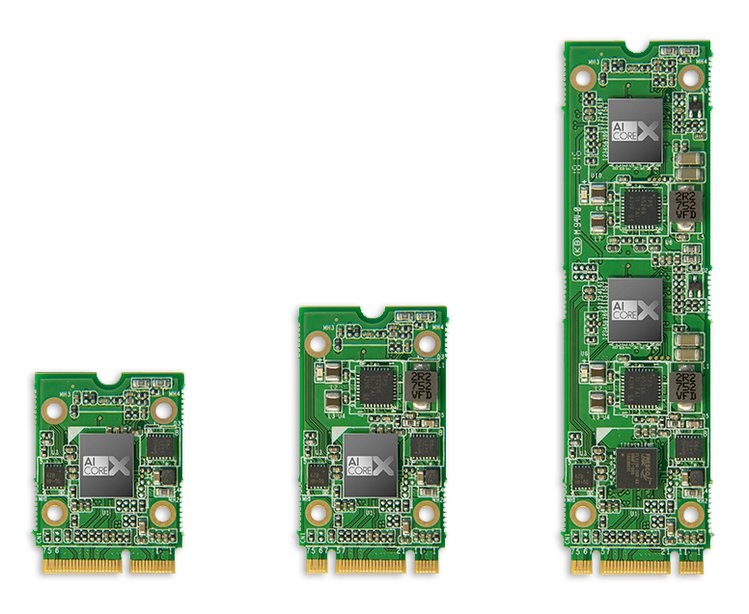
Neural network accelerator for AI on the edge. Up to four trillion ops/sec with just a few watts. Neural Networks are the future of AI and these boards comes into play to help you develop your intelligent visual system with ease.
UP AI CORE X is a complete product line of neural network accelerators for edge devices. Whether the automation you are creating is for identifying and tallying items in a shopping cart, alerting airport security to unattended luggage, or monitoring traffic congestion ahead of an autonomous vehicle, the AI CORE X let’s you embed the real-time computational power you need directly where you need it.
The AI CORE X is powered by the recently released Intel® Movidius™ Myriad™ X, a third-generation vision processing unit (VPU) that is the first in its class to include a Neural Compute Engine – a dedicated hardware accelerator for deep neural networks, trainable with industry-standard tools.
AI CORE X is available with one or two Myriad X chips in a variety of form factors. With your choice of MiniCard/mPCIe, M.2 2230, M.2 2242, M.2 2280, or a custom form factor, embedding deep learning capabilities has never been easier.
The UP AI Core X is currently raising on Crowd Supply, with pricing at $94 for the single-core mPCIe, M.2 2230 E key, and M.2 2242 B+M key, AI Core X and XM boards, and $144 for the dual-core M.2 2280 M+B key AI Core XM board.
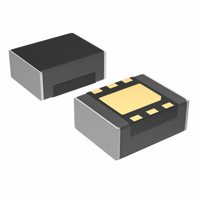
The XCL206 series is a synchronous step-down micro DC/DC converter which integrates an inductor and a control IC in one tiny package (2.5mm×2.0mm, H=1.0mm). A stable power supply with an output current of 600mA is configured using only two capacitors connected externally. Operating voltage range is from 2.0V to 6.0V(XCL20xG:1.8V-6.0V). Output voltage is internally set in a range from 0.8V to 4.0V in increments of 0.05V. The device is operated by 3.0MHz, and includes 0.42ΩP-channel driver transistor and 0.52Ω N-channel switching transistor. As for operation mode, the XCL206 series is automatic PWM/PFM switching control , allowing fast response, low ripple and high efficiency over the full range of loads (from light load to heavy load). During stand-by, the device is shutdown to reduce current consumption to as low as 1.0μA or less. With the built-in UVLO (Under Voltage Lock Out) function, the internal driver transistor is forced OFF when input voltage becomes 1.4V or lower. XCL206B(G,F)series provide short-time turn-on by the soft start function internally set in 0.25 ms (TYP).XCL206B(C,G,F) integrate CL auto discharge function which enables the electric charge stored at the output capacitor CL to be discharged via the internal auto-discharge switch located between the LX and VSS pins. When the devices enter stand-by mode, output voltage quickly returns to the VSS level as a result of this function.
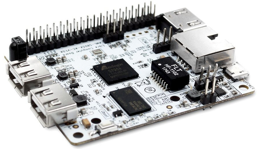
Libre Computer has successfully launched a smaller, less powerful follow-up to its Le Potato SBC, the “La Frite SBC. The La Frite SBC is a small version of the Le Potato SBC, that has a quad -A53, HD-only Amlogic S805X, a Raspberry Pi A+ footprint and GPIO connector, and mainline Linux support. The 64 x 55mm La Frite is roughly modeled on the 65 x 56mm Raspberry Pi Model A+. The new board has a different layout and more real-world ports than the Pi model A+, although it has a similar 40-pin expansion header like the A+.
Libre La Frite
The La Frite comes in different configurations, that starts at just $10 or $15 for models with 512MB or 1GB DDR4, respectively. Fully fitted models with 8GB eMMC, HDMI cable, and a 2.5A power supply with LED and power button go for $30 or $35. Shipments will start in November 2018. The La Frite is powered by a 1.2GHz S805X version of the quad-core, Cortex-A53 Amlogic S900. This is lower power, compared to the 1.5GHz S905X model found on Le Potato. The SoC has the same Mali-450 GPU but is limited to 1080p video encode and decode rather than 4K on Le Potato.
Other features include a low-profile 10/100 “Fast” Ethernet port plus 2x USB 2.0 ports and a micro-USB OTG with power input. The display port is listed as HDMI 2.0 port on the product page but listed as HDMI 1.4 port on KS. There’s also an IR receiver, but for WiFi connectivity you have to use one of the USB ports.
La Frite supports Ubuntu, Debian, LibreELEC, Lakka, RetroPie, Android Oreo, other Linux based distributions. Libre Computer has collaborated with BayLibre, which recently demonstrated a hardware accelerated codec running on Chromium through the V4L2 Linux subsystem on Amlogic’s S900. This means Soon, Le Potato and La Frite will be able to play H.265, H.264, and VP9 content on upstream Linux with Chromium for the first time.
The La Frite SBC also support Arm’s upcoming EBBR (Embedded Base Boot Requirements) boot specifications for the ARM64 kernel, which defines a part of UEFI that can be applied with upstream U-Boot. La Frite includes 128Mb of SPI NOR flash to enable booting of Linux with EBBR. This will likely give room for “customized booting of upstream Linux from various sources including USB flash drives, USB hard drives, and PXE.” The SBC is also equipped with a U-Boot button.
Specifications listed for La Frite include:
Processor: Amlogic S805X (4x Cortex-A53 @ 1.2GHz); 650MHz Mali-450 GPU (pentacore 2G + 3P) with OpenGL ES 1.1/2.0 and OpenVG 1.1; Amlogic Video Engine 10 with VP9, H.265, and H.265 1080p60 decode and H.264 1080P30 encode
Memory/storage: 512MB or 1GB DDR4 RAM, 128Mb SPI NOR, eMMC 5x interface with optional 8GB
Networking: 10/100 Ethernet port (low profile)
Other I/O: HDMI port with HD output and optional cable, 2x USB 2.0 host ports, Micro-USB OTG port with power input, 40-pin low-speed header (PWM, I2C, SPI, GPIO)
Other features: IR receiver; U-Boot button
Power: 5V via micro-USB; optional 2.5A power supply with LED and power button
Operating system: Mainline Linux with support for Ubuntu, Debian, LibreELEC, Lakka, RetroPie, Android Oreo, and more.
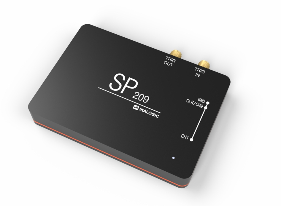
SP209 series logic analyzers and protocol decoders offer in depth analysis of logic signals and protocols with 200MHz (5ns) timing resolution. 9-channel operation allows 8-bit parallel data to be captured along with a clock or strobe signal. SP Series is composed of two devices, SP209 and SP209i: The SP209 is the standard edition and SP209i is the industrial one with some additional features, like: Logic channels can be multiplexed with dedicated industrial inputs that can be directly connected to: RS232, RS485, CAN and LIN buses.
SP209 series logic analyzers rely on ScanaStudio software (runs Windows, Mac and Linux) to capture, display, analyze and decode signals. Most industry standard protocols can be interpreted, among which: SPI, I2C, USART, 1-Wire, CAN, LIN, I2C, RS232, RS485, TWI and much more (click for full list of supported protocol decoders).
Features
9 logic channels with adjustable thresholds (1.8V, 2.5V, 3.3V, 5V)
State of the art input stage, with Schmitt triggers that eliminate glitches on slow signals
200 MHz sampling rate, with all 9 channels used.
External clock option (state mode), up to 50MHz
Precise trigger-In and trigger-Out signals on SMA ports
Samples compression and streaming via USB.
2Gb DDR-3 memory kicks-in when USB isn’t fast enough.
Embedded receivers on industrial version: SP209i (RS232, CAN, LIN, RS485).
Guaranteed performances on all hosts.
The standard edition costs 299€ with a -50€ discount on pre-orders.
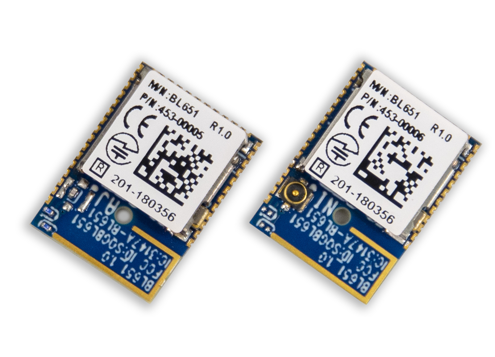
Laird’s BL651 Series contains the latest Nordic nRF52810 silicon with Bluetooth 5 Low Energy capabilities and groundbreaking ultra-low power performance. Building on Laird’s multi generation module developments utilizing Nordic silicon (BL600, BL652, BL654) – now comes the latest series offering cost effective Bluetooth 5 enablement for simple BLE applications.
The BL651 series exposes all the capabilities of the Nordic nRF52810 silicon in a small, fully certified module with simple soldering castellation for easy prototyping and mass production manufacturing. Use the Nordic SDK & SoftDevice or Zephyr Project to deliver your BLE application.
In addition the BL651 series is 100% PCB footprint drop in compatible with the BL652 Series of modules.
Features
Bluetooth v5.0 – Single mode
External or internal antennas
Application development via Nordic SDK or Zephyr
Compact footprint (pin compatible with BL652)
Programmable Tx power +4dBm to -20dBm
Tx whisper mode (-40dBm)
Rx sensitivity: -96dBm
Ultralow power consumption
Tx: 4.6mA peak (at 0dBm, DCDC on)
Rx: 4.6mA peak (DCDC on)
The modules will be available on late October 2018.
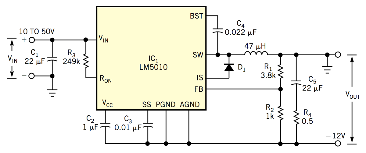
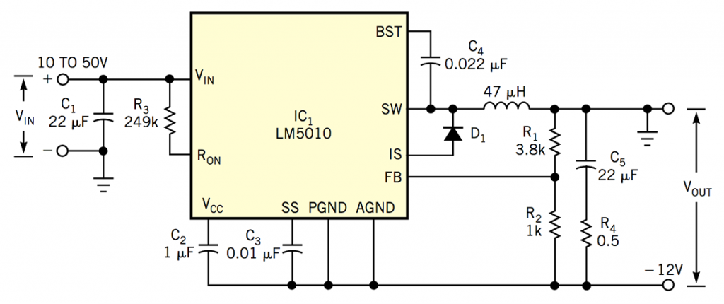
Based on National Semiconductor’s LM5010, this buck-boost regulator operates over a wide input-voltage range.
This is a LM5010 buck-boost regulator able to convert a positive input ranging from 10-50Vdc to -12V output. by Robert Bell @ www.edn.com
Buck regulators find wide application as step-down regulators for converting large positive input voltages into a smaller positive output voltages. Figure 1 shows a simplified buck regulator that operates in continuous-conduction mode—that is, the inductor current always remains positive. The output voltage, VOUT, is equal to D×VIN, where D is the duty-cycle ratio of the buck switch, Q1, and VIN is the input voltage. The duty cycle, D, is equal to TON/TS, where TON is the on-time of Q1 and TS is the switching-frequency period.
Figure 3 shows a low-cost buck-boost converter based on the LM5010 buck-regulator IC that converts a 10 to 50V positive supply voltage into –12V. Although many applications use a fixed switching frequency and modulate the output pulse width, this design features a constant-on-time approach in which the IC’s internal output transistor turns on for an interval that’s inversely proportional to the difference between the circuit’s input and output voltage.
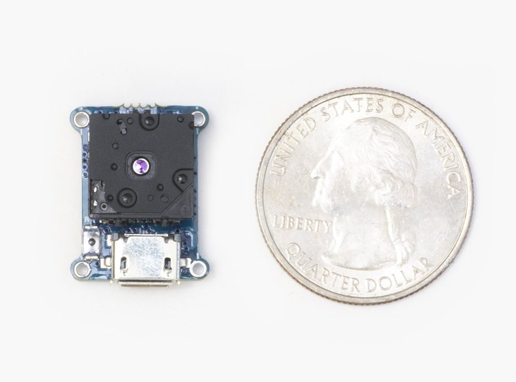
PureThermal Mini is a hackable thermal webcam for the FLIR Lepton (2.x – 3.x) LWIR camera core. It is the result of listening to our thousands of PureThermal 1 users and giving them what they want: four mounting holes, pads for optional EM shielding, less complex circuitry, and perhaps best of all, USB DFU. That’s right, a JTAG breakout board will no longer be required to update PureThermal 2. This is a development kit ready to be embedded into a production system.
STM32F412 ARM microprocessor. Execute on-board image processing without the need for an external system or SBC.
USB UVC works on Windows, Linux, Mac, and Android.
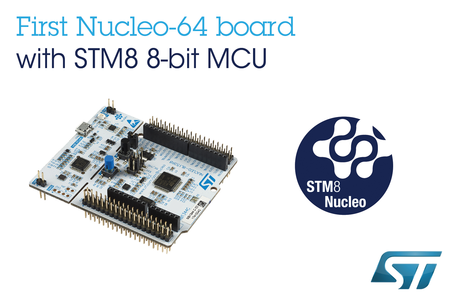
STMicroelectronics has introduced two STM8* Nucleo development boards, letting the 8-bit world experience the ease of access and extensibility already proven with the STM32* Nucleo range.
Leveraging the formula that has kickstarted countless STM32 embedded projects, the STM8 Nucleo boards give full access to all STM8 MCU I/Os through ST morpho headers, and contain Arduino™ Uno connectors that simplify functional expansion by accessing the vast ecosystem of open-source Arduino-compatible shields.
The two STM8 Nucleo boards are supported by major development toolchains including the Cosmic IDEA toolchain, the IAR™ EWSTM8 Integrated development environment, and the free STVD IDE from ST. Support for convenient features like drag-and-drop Flash programming accelerates design iterations. Each board comes with an integrated ST-LINK debugger/programmer, which eliminates any need for a separate debug probe.
By adding these entry-level STM8 configurations, over 40 Nucleo boards are now available, covering the full spectrum of performance, power, and memory combinations across ST’s complete families of 8-bit and 32-bit microcontrollers. Product creation is fluid and flexible, conveniently connected to open-source hardware communities, with freedom to adjust or optimize hardware and software at any time thereby eliminating risk and helping minimize time to market.
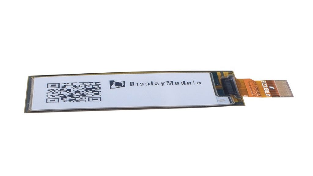
DisplayModule introduced a tiny 2.1″ E-paper display with 212×104 pixels resolution. The display can be interfaced using SPI and a Raspberry Pi shield is available for the ones that what to connect it to the popular SBC.
Features
Flexible and 0.3mm thickness E-Paper
2.13 Inch is suited to E-Label or wearing equipment.
212×104 resolution E-Ink raw display
No back-light, keeps displaying content forever even no power supply
Easy to use, displays any contents via SPI interface, including geometric graphics, texts, and images
Ultra low power consumption, basically power is only required for refreshing
It is easy working on Raspberry Pi with DM-ADTPI-013( RESE:A; BS:0)
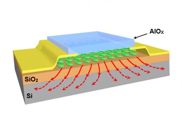
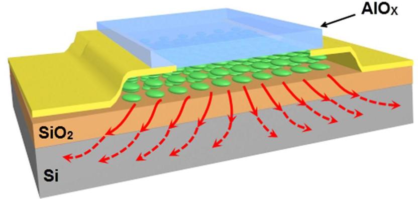
A new study about “Reduction of overheating of 2D materials” published in the Journal of Advanced Materials. The work put behind the study is credited to the researchers at the University of Illinois at Chicago College of Engineering. By joining together two-dimensional materials used in nanoelectronic devices between their three-dimensional silicon bases, they formed an ultrathin layer of Aluminium Oxide which can significantly reduce the risk of component failure due to overheating.
Modern silicon-based electronic components use 2D materials such as graphene. These materials are formed of a single-atom-thick layer of carbon atoms. They are used into the electronics components which allows them to be several orders of magnitude smaller than if they were made with conventional 3D materials. These 2D materials enable many unique functionalities in those 3D nanostructures. But the main drawback of using this kind of material junction is that they prone to overheat and lose their performance.
In the field of nanoelectronics, the poor heat dissipation of 2D materials has been a bottleneck to fully realizing their potential in enabling the manufacture of ever-smaller electronics while maintaining functionality,
-stated Amin Salehi-Khojin, associate professor of mechanical and industrial engineering in UIC’s College of Engineering.
One of the most important reasons that 2D materials can’t efficiently transfer heat to silicon is that the interactions between the 2D materials and silicon in components are rather weak. Bonds between the 2D materials and the silicon substrate are not very strong, so when heat builds up in the 2D material, it creates hot spots causing overheat and device failure.
To enhance the connection between the 2D material and the silicon base to improve heat conductance, engineers have experimented with adding an additional ultra-thin layer of material on top of the 2D layer. It creates a “Nano-sandwich” with the silicon base and ultrathin material acting as the “bread”. By adding another ‘encapsulating’ layer on top of the 2D material, they have been able to double the energy transfer between the 2D material and the silicon base.
Salehi-Khojin and his colleagues have created an experimental transistor using Silicon Oxide for the base, carbide for the 2D material and Aluminum Oxide for the encapsulating material. At room temperature, the researchers saw that the conductance of heat from the carbide to the silicon base was twice as high with the addition of the Aluminum Oxide layer versus without it.
While our transistor is an experimental model, it proves that by adding an additional, encapsulating layer to this 2D nanoelectronics, we can significantly increase heat transfer to the silicon base, which will go a long way towards preserving the functionality of these components by reducing the likelihood that they burn out,
said Salehi-Khojin. Their next steps will include testing out different encapsulating layers to see if they can further improve heat transfer.