Intel releases seven NUCs with Coffee Lake and 10nm Canyon Lake CPUs

Despite struggles and delays with its 10nm processor, Intel has finally released five NUCs (Next Unit of Computing) mini-PC kits that comes with 14nm, 8th Generation Coffee Lake CPU. It also released two NUCs that comes with its 10nm Cannon Lake chips and comes configured with Windows 10 with shipments to begin in October or November. The coffee lake NUC supports any Intel-ready OS including Linux and Windows and they come in barebones kits with RAM and Storage. The windows 10 Home powered crimson Canyon lake NUCs are among the first products that comes with a dual-core, 15W TDP core i3-8121U coffee lake CPU aside from a new version of a Lenovo IdeaPad 330 laptop.

Intel’s Bean Canyon NUC

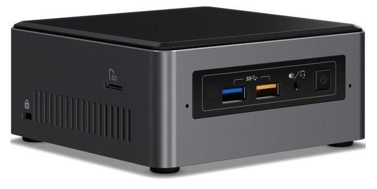
The five new Coffee lake powered Bean Canyon NUCs comes with H-, M- and T- series Intel core chips and share many of the features as the Baby Canyon NUCs released earlier in April. They also have CPUs with 28W TDPs and supports up to 32GB dual channel DDR4-2400 RAM. They feature Intel’s fastest graphic chip- compared to the desktop models- known as the Iris Plus 655 graphics with 128MB eDRAM. The increased eDRAM stands out from previous parts that just supports 64MB eDRAM cache which delivers better graphic performance and can be used as general cache. The various options available for the five NUCs are:

  • NUC8i7BEH (Core i7-8559U)
  • NUC8i5BEH (Core i5-8259U)
  • NUC8i5BEK (Core i5-8259U)
  • NUC8i3BEH (Core i3-8109U)
  • NUC8i3BEK (Core i3-8109U)

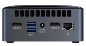
The Bean canyon NUCs comes with an HDMI 2.0a host port with resolution up to 4096 x 2304 and 7.1 surround sound audio. There’s also a Thunderbolt 3 port which supports USB 3.1 Gen 2 (with speed up to 10Gbps) and can be used as a DisplayPort 1.2 connection. It also includes four USB 3.1 host ports (one of the ports supports charging) and two USB 2.0 headers.

The Bean Canyon NUCs are also equipped with Bluetooth 5.0, Intel Wireless AC 9560, dual GbE ports, a 12-19VDC input, power button, a MicroSD slot, 3.6mm audio jack and a support for Kensington lock.

The Crimson Canyon NUCs with Cannon lake chips no doubt gives us a glimpse of future Intel 10nm generation of chips. These game oriented NUCs comes in two models- Crimson Canyon NUC8i3CYSM (has 8GB of LPDDR4-2400) and NUC8i3CYSN (has 4GB of LPDDR4-2400) and it is built with windows 10 Home and like another windows PC, it can be swapped with Linux.

Intel’s NUC crimson canyon

The Crimson Canyon NUCs powered by Intel Cannon lake chips is accompanied by AMD’s discrete Radeon 540 GPUs with Integrated 2GB of GDDR5 Memory which makes it different from the Bear Canyon NUCs’ integrated Iris graphics.

Both Crimson Canyon Models are very similar to the Bean Canyon NUCs with the only evident difference is the addition of a second HDMI 2.0 port instead of a USB Type-C DisplayPort.

These intel NUCs are good options for casual users and the high graphics performance can allow to stream and play eSports games and users should be ready to spend extra cash on storage and memory as these NUCs are just Barebone kits.

Meanwhile they are reports have leaked about a new 14nm 9th Gen core chip family which Intelis expected to release in October.

Check Intel’s NUCs kit page for full spec

Keysight Keysight UXR 110GHz BW, 256GS/s, 10-bit, 4-Channel Real-Time Oscilloscope Teardown & Experiments

In this episode Shahriar takes a look at one of the most advanced electrical test and measurement instruments ever created. The Keysight UXR-Series Real-Time Oscilloscope brings 110GHz of analog bandwidth and 256GS/s real-time sampling at 4-channels simultaneously. To make it even more impressive, the entire data-conversion architecture is in 10-bits. This implies that the instruments captures, processes, stores and displays over 10Tb/s of information.

Various architectures of state-of-the art oscilloscopes from Keysight, LeCroy and Tektronix are examined and compared against the new real-time architecture of the UXR-Series oscilloscope. The teardown of the front-end 110GHz module along with the data acquisition board is presented and analyzed in detail. The instrument showcases a wide range of Keysight technologies implemented in various technologies such as InP, SiGe BiCMOS, 65nm CMOS and 28nm CMOS nodes. In combination with Hyper-Cube memory module, data can be captured at 256GS/S from all 4-channels at the same time. Several variants of the UXR-Series oscilloscope will be available from 13GHz to 110GHz bandwidths.

Keysight Keysight UXR 110GHz BW, 256GS/s, 10-bit, 4-Channel Real-Time Oscilloscope Teardown & Experiments – [Link]

ArdOsc – Arduino Oscilloscope in a Matchbox

Peter Balch @ instructables.com build an Arduino based tiny oscilloscope and a detailed explanation is given on the tutorial. He writes:

Why would I want a tiny oscillscope? I’ve got a room full of electronic Stuff including four oscillscopes. But it’s a fuss using them. It would be nice to have something that fits in my pocket, that sits next to the circuit I’m working on and that’s as easy to use as a multimeter.

This oscilloscope costs the price of an Arduino Nano (£2 and a display (£3) plus a few pence for resistors, etc. It’s specification is:

ArdOsc – Arduino Oscilloscope in a Matchbox – [Link]

Sensything Provides Sensors, Processing, and Wireless on a Single Board

Multi-sensor data acquisition, processing, and Wi-Fi/Bluetooth communication in a single, open source board. Sense anything.

Sensything is an open source, high-resolution (24-bit), Wi-Fi and Bluetooth-enabled sensor interface platform that supports multiple sensor readings. In most cases, it offers a single-board, single-platform solution for acquiring and logging multiple sensor readings that can be seen/sent through an Android app, an IoT or analytics platform, or over an ordinary USB connection.

Sensything is based on the popular ESP32 SoC for IoT applications and includes the ADS1220 24-bit ADC that provides low-noise data acquisition. It provides all the accompanying components, including a Li-ion battery and an on-board,low-noise, five volt power source for reliable low-noise performance. Additionally, extra GPIO pins and support for Sparkfun’s Qwiic connector standard makes multi-modal sensor data fusion and recording easy.

The project is live on Crowdsupply and has 36 days to go.

DIY NAS / Router in 3-bay hot swap enclosure

A 2-bay, low power, ARM-based NAS and router. The project repository is here.

The enclosure is an Athena Power BP-SAC2131B 3.5” HDD Hot-Swap Backplane Module. This is a a 3-bay hot swap backplane intended to go into two 5.25” bays of a server. This is not a trayless backplane, the hard disks must be mounted using four included screws.

This is a 3-bay case, but I only need the top two bays for hard drives. In the bottom bay I will put the computer that runs the NAS. Something like a Pico-ITX or 3.5” SBC computer will fit within the footprint of a hard dive.

The main problem with using an internal enclosure as a case is that all the SATA connections ago out the back of the case, not internal for connections to a computer.

Luckily there is a slot on the back of the case. Using something like these very thin blue SATA cables, I can connect an internal computer to the back of the case

  • Cost less than a cheap commercial 2-bay NAS (~$200)
  • Low power
  • NAS for local file sharing
  • A limited router to segregate scary “smart” devices on the LAN
  • Maybe run some IoT things

DIY NAS / Router in 3-bay hot swap enclosure – [Link]

Easy Motion and Gesture Detection by PIR Sensor & Arduino

Here we use PIR sensor and Arduino to detect the motion of a hand. This detection can be used to operate electronic equipment. By ElectroPeak @ hackster.io:

In this article, we’ll show you how to make a gesture detector by simple components like PIR sensor and Arduino Nano. At the end of this article you can:

  • Explain PIR sensor applications and how it works
  • Run an 8-Pixel PIR sensor named TPA81
  • Use PIR sensor to detect motion and gesture by Arduino
  • Make a cool detector to increase or decrease your speaker volume

Easy Motion and Gesture Detection by PIR Sensor & Arduino – [Link]

Programming Atmega328p Microcontroller with Arduino IDE

Introduction

Over the past few tutorials, we have mentioned several scenarios where using any of the Arduino board in a project may be an overkill due to the cost, size, and more technical reasons such as high power consumption. In the last tutorial, we discussed an alternative way of using Arduino, i.e. using the Atmega328p microcontroller alone which removes all the downsides of using the Arduino board, while retaining one of the biggest benefits of the Arduino platform; the ease of programming.

Atmega328p Microcontroller

We covered details on preparing the Atmega328p microcontroller for programming by flashing the Arduino bootloader on Atmega328p and today’s tutorial will be a follow up to that tutorial, as we will look at how to program the boot-loaded Atmega328p microcontroller using the Arduino IDE.

The Atmega328p microcontroller, like any other microcontroller, can be quite tasking to use for a beginner. They usually require a certain set of tools, including a programmer (hardware), and a development platform (e.g Atmel Studio) for writing code. These development platforms, unlike the Arduino IDE usually require high knowledge of C or other programming languages, without the shortcuts and simplified functions which the Arduino provides.

To remove this difficulty, the microcontroller is flashed with the Arduino bootloader, which makes it ready for programming using the simpler and easy to use Arduino IDE.

To program the microcontroller using the Arduino IDE, the microcontroller must be connected via some sort of hardware to the computer. This is usually done via two major ways:

  1. Using a USB to Serial/TTL Adapter
  2. Using an Arduino board

Each of these approaches provides the microcontroller with an interface that enables interaction between the computer and the microcontroller.

We will take each of these approaches one after the other and look at the components and setup required to upload code to the microcontroller.

Using a USB to Serial/TTL Adapter

USB to Serial/TTL Adapter

The first approach involves the connection of a USB to serial adapter to the microcontroller. The USB to Serial/TTL adapter converts data signals from the USB on the computer to serial/TTL for the microcontroller and vice versa. This enables communication from the microcontroller (serial) with the Arduino IDE running on the PC (USB). This setup, compared to the second one, is by far the cheapest, as these adapters are usually very cheap.

Required Components

The following components are required for this approach;

  1. Atmega328P microcontroller with the Arduino Bootloader installed
  2. Breadboard
  3. USB to serial/TTL Adapter
  4. 16MHz crystal oscillator
  5. 22pf capacitors  x2
  6. 100nf capacitor
  7. Jumper Wires
  8. 100 ohms resistor
  9. LED

Schematic

Connect USB to Serial/TTL adapter to the microcontroller as shown in the schematics below. Don’t forget that this procedure will only work if the microcontroller has been flashed with a bootloader according to the procedure described in the last tutorial.

Schematics 1: USB to Serial Adapter and the Atmega328P

Most adapters can be configured to work at either 5v or 3.3v logic level. Ensure yours is configured to work on the 5v voltage level since supply to the microcontroller is 5v.

Uploading Code

Uploading code to the microcontroller after you are done with the connections, require no additional work asides, what you would have done if you where using an Arduino board. After typing in your code, select the port to which your adapter is connected, followed by the board type and hit the upload button. Upload takes only a few seconds, same as the Arduino board.

Note: when programming the Atmega328p MCU using the Arduino IDE, the matching board type you have to select is the “Arduino Duemilanove or Nano w/ ATmega328” board.

To test the setup, we will use the Arduino blink example. Select the example and click upload. You should see the connected LED start blinking after a while.


Using an Arduino Board

The second approach involves the use of an Arduino board in either of two similar ways;

  1. By replacing the microcontroller on the Arduino Uno with the one to be programmed
  2. By using any of the Arduino boards as an In-system programmer.

The first mode is the easiest way to upload code to the microcontroller, as it involves just replacing the microcontroller on the Uno, with the one to be programmed. However, this may not be the best when prototyping as the move of the chip from the Arduino to the project, back and forth, could lead to the pins of the microcontroller being damaged. Another downside to this is that it only works with the Arduino Uno as all other Arduino boards, use SMD type of microcontrollers which makes replacement impractical and development, expensive.

So no schematic for this, just swap the microcontroller and hit upload.

The second method involves the use of the Arduino Uno as an In-system programmer.

Required components

To use this approach, you will need the following components;

  1. Arduino Uno
  2. Breadboard
  3. USB to serial/TTL Adapter
  4. 16MHz crystal oscillator
  5. 22pf capacitors  x2
  6. Jumper Wires
  7. 10k resistor
  8. 100 ohms resistor
  9. LED

Schematics

Connect the components as shown in the schematics below.

Programming Atmeg328p with the Arduino Uno

While using this approach, it is important to remove the microcontroller of the Arduino board to prevent interference.

Upload Code

Code upload process is the same as already described. Type the code to be uploaded or select an example -> select the board type (Duemilanove or Nano W/atmeg328), select the correct port and click upload. The code will be uploaded to the microcontroller.

After successful code upload using any of the approaches described above, the Arduino or USB – Serial/TTL converter can be disconnected and the project connected to a battery to run on standalone as shown in the image below.

Programmed Atmega328p Microcontroller

That’s it for this tutorial guys, thanks for following.

Feel free to drop questions and comments under the comment section, I will do my best to respond to them asap.

Till next time!

Rock960 SBC- A viable Competitor to Raspberry PI

The Rock960 SBC –  developed by Guangzhou based startup called Varms – is built on the hexa-core Rockchip RK3399 and it really stands out from other SBC contenders like the NanoPI M4 despite being a little pricy. The Rock960 is the only “96boards’s SBC” in the market that is built on the popular Rockchip hexa-core SoC and serves as a powerful alternative to Raspberry Pi. This SoC comes with dual Cortex-A72 and quad Cortex-A53 cores. It also comes with a Mail-T860 MP4 GPU which supports H.264 10bit and VP9 4k video and it is the highest performance GPU built on ARM famous Midgard Architecture. Regarding storage, it comes with 2GB RAM, 16GB eMMC or 4GB RAM, 32GB eMMC.

The Rock960 also supports various open source operating systems such as Android 7.1 AOSP, Debian, Ubuntu, Fedora, LibreELEC, Lakka and FlintOS. Schematics and other hardware files are posted on the community website which also says it supports Yocto and Armbian.

Despite being one of its kind, it comes with its own challenges. One of the challenges is that the board’s M.2 expansion slot is not in a good position to mount NVMe SSD – says Varms –  but the company has provided an optional M.2 Extend board which does not affects the performance of the NVMe SSD. It also has the option to add a metal case -in several colors like opaque, transparent or semi-transparent top- that adds additional heatsink properties in addition to the standard heatsink.

Rock960 board - front view
Rock960 board – front view

Compared to other boards that comes with the Rockchip RK3399 like the Firefly-RK3399 and VS-RK3399, Rock960 is both simpler and smaller and comes in 85mm by 55mm dimensions. The company also offers various “96Boards” expansion connectors like the standard 40-pin low-speed and 60-pin high-speed connectors. There is also a growing list of third-party “96Boards” expansion boards.

The Rock960 has a built in HDMI 2.0 port and a DisplayPort (via a USB Type-C port), both with 4K@60fps video. MIPI-DSI display and MIPI-CSI camera connections are also available along with USB 3.0 and 2.0 host ports and a microSD slot.

The Rock960 board also comes in an Enterprise Edition which has similar specs to desktop PCs and it is suitable for those using 3D graphics and Machine learning applications. It is built on a hexa-core processor, packed with a powerful GPU and a dedicated Neural Processing Unit capable of 2.4TOPS (Trillion Operations Per Second) and it has shown it beats both the Apple A11 chip and Kirin 970 SoC in benchmarking.

The Rock960 Enterprise Edition Boards has a 3 USB 3.0 and 5 USB 2.0 ports, dual SATA 3.0 ports, upto 8GB RAM and supports expansion boards through its PCI x16 slot.

For easier development of vision and speech applications, Rockchip collaborated with Open AI Lab to port open source AID (Artificial Intelligence for Development) on the Rock960.

Find the full detailed specifications for the Rock960 SBC Consumer Edition as listed on Varms shopping page:

Components  Description
Processor Rockchip RK3399
CPU ARM Cortex-A72 Dual-core up to 1.8GHz + Cortex A53 Quad-core up to 1.4GHz
GPU ARM Mali T860MP4
RAM 2GB or 4GB LPDDR3 @ 1866MHz
PMU RK808-D
Storage 16/32GB eMMC 5.1
Ports Ethernet, USB 2.0/3.0 expansion
Wireless WLAN 802.11 ac/a/b/g/n, 2xMIMO, 2.4GHz and 5Ghz, Bluetooth 4.2. On board WLAN/BT antennas.
USB 1 x USB 3.0 type A and 1 x USB 2.0 type A (host mode only) and 1 x USB 3.0 type C OTG
Display 1 x HDMI 2.0(Type A – full) up to 4Kx2K@60Hz, 1 x 4L – MIPI DSI up to 1080p@60Hz, 1 x DP 1.2(Type C) up to 4Kx2K@60
Video Inside decoder: H.264 10bit up to HP level 5.1 – 2160p@60fps (4096×2304), VP9 – 2160p@60fps(4096×2304), H.265/HEVC 10bit – 2160p@60fps(4096×2304), MPEG-1, MPEG-2, MPEG-4, H.263, VP8, VC-1.
Audio HDMI output
Camera 2 x 4-lane MIPI CSI
Expansion Interface 40 pin low speed expansion connector: +1.8V, +5V, DC power, GND, 2UART, 2I2C, SPI, I2S, 12xGPIO and 60 pin high speed expansion connector: 4L-MIPI DSI, I2C x2, SPI (48M), USB 2.0, 2L+4LMIPI CSI
LED 1 x WiFi activity LED(Yellow), 1 x BT activity LED (Blue) and 4 x User LEDs (Green)
Button Reset button, recovery button
Power Source Recommend a 12V@2A adapter with a DC plug which has a 4.75mm outer diameter and 1.7mm center pin with standard center-positive (EIAJ-3 Compliant)
OS Support AOSP, Debian, Ubuntu, Fedora, LibreELEC, Lakka, FlintOS
Size 85mm x 55mm

The 2GB RAM, 16GB eMMC model is available for $99 while the 4GB RAM, 32GB model is available for $139 on Vamrs page.

WarpPi is a Hackable Raspberry Pi Algebra Calculator

Have you ever been given an algebra homework where there were a problem and its answer, but you couldn’t figure out how they went to the solution? Well, you’re in luck! With Andrea Cavalli’s WarpPi calculator and its CAS (Computer Algebra System), you can go ahead and build your own algebraic calculator and even modify it to your taste.

Algebra is a rather broad part of mathematics dealing with variables, equations, functions, exponents and so on. For an area as broad, one would fittingly expect different levels of complexity. The calculator by Andrea Cavalli is specifically designed to aid one in solving such complex algebraic problems and goes a step further from commonly used scientific calculators.

The good thing is, you can build Andrea Cavalli’s DIY WarpPi calculator and set it up to your specific needs.

The calculator stands out with a custom Printed Circuit Board (PCB) and a neat 3D printed case and buttons. Its runs on custom software written in Java which brings the power of Java to real-time applications. At the heart of the calculator is a portable Raspberry Pi Zero W which hooks right into the PCB. One fantastic thing about this calculator is its ability to provide step by step solutions to algebraic problems.

On the board is also  a power management module for the device, which includes the physical power switch, a USB connection for charging, and a linear regulator. One interesting feature about the WarpPi is the presence of a hatch to access the Raspberry Pi’s micro SD card which will inevitable makes it easier to alter software configurations without dismantling the calculator.

The WarpPi 3D printed case might be a bit confusing for some users because the 3D printed case lacks any form of markings to indicate the functionality that each button controls, however, users can quickly figure out what each key does using a demo live preview built by Andrea Cavalli here.

Unlike your everyday average scientific calculator, Andrea Cavalli’s WarpPi calculator can be programmed to do a wide range of other mathematical computations as you deem fit. Its true potential can only be unlocked by how creative you can get. If you are considering building one yourself, the 3D-printed case, the guides, and code to run it are all available on the WarpPi GitHub page. If you eventually make yours, don’t forget to improve it as well.

Imec Invented Unique Cost-effective Cooling For High-Performance Chips

Imec, the distinguished Belgian research center has invented a new and cost-effective method of cooling chips. This achievement can be an important innovation to tackle the ever-increasing cooling demands of high-performance 3D chips and systems.

Present powerful electronic systems have high cooling demands for integrated semiconductor chips. Conventional solutions operate with various passive (or occasionally active) heat sinks. The main bottleneck in the heat-transfer path occurs at the interface between the semiconductor and the heat sink. It is proven that direct cooling on the back of the chip is more efficient, but current microchannel solutions do more harm than good. It leads to stress and a temperature gradient across the chip surface. Thus a new way of cooling in that method was much needed.

Imec's cost-effective cooling solution for high performance chips
Imec’s cost-effective cooling solution for high-performance chips

The ideal solution is to use an impingement-based cooler with coolant outlets distributed across the chip’s surface area. This system directs the liquid perpendicular to the chip surface and ensures the liquid is at the same temperature throughout. It also reduces contact time between the coolant and the chip. Until now, cooling solutions based on this principle have the disadvantage of being very expensive. In some other alternative implementations, the nozzle diameter and necessary fabrication techniques are not compatible with chip packaging processes.

Imec has developed a new impingement chip cooler that uses polymers instead of silicon, to achieve a cost-effective fabrication. Moreover, imec’s solution features nozzles of only 300µm diameter, made by high-resolution stereolithography 3D printing. The use of 3D printing allows customization of the nozzle pattern design to match the heat map and the fabrication of complex internal structures. Moreover, 3D printing allows to efficiently printing the whole structure in one part, reducing production cost and time.

Schematic of multi-jet cooler

Our new impingement chip cooler is actually a 3D printed ‘showerhead’ that sprays the cooling liquid directly onto the bare chip,” explains Herman Oprins, senior engineer at imec. “3D prototyping has improved in resolution, making it available for realizing microfluidic systems such as our chip cooler. 3D printing enables an application-specific design, instead of using a standard design.

Imec’s impingement cooler achieves a high cooling efficiency, with a chip temperature increase of less than 15°C per 100W/cm2 for a coolant flow rate of 1 l/min. Moreover, it features a pressure drop as low as 0.3 bar, because of the smart internal cooler design. It outperforms benchmark conventional cooling solutions in which the thermal interface materials alone already cause a 20-50°C temperature increase. It is a highly efficient and cost-effective fabrication. Imec’s cooling solution is much smaller compared to existing solutions, matching the footprint of the chip package enabling chip package reduction and more efficient cooling.

TOP PCB Companies