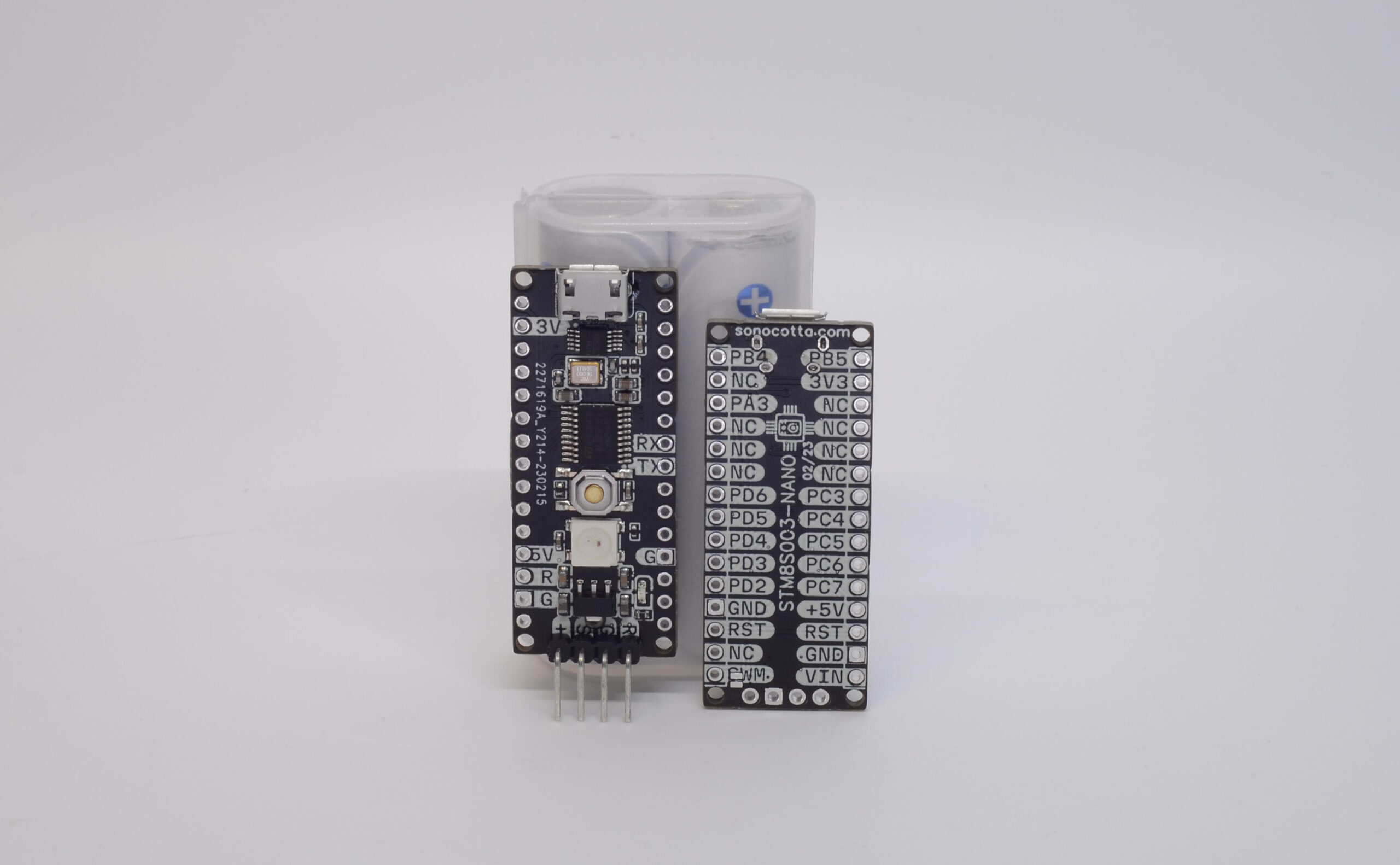
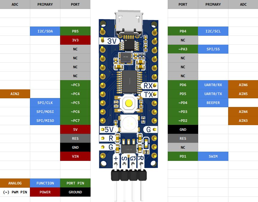
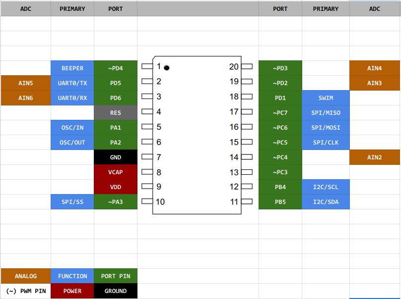
Andriy Malyshenko, a cloud architect and self-described “maker and tinkerer at nights,” has taken up the challenge of addressing component shortages during the chip crisis. In response to the inflated prices of Microcontroller Units (MCUs) due to the shortage, Malyshenko sought out affordable and readily available alternatives. His efforts have resulted in the creation of the STM8S003 Development Board, a compact and Arduino Nano-sized board based on the STM8S003F3 microcontroller. This board offers not only reasonable performance and low power consumption but also a range of features, including a 16MHz clock speed, 8kB of flash memory, 1kB of RAM, and 128 bytes of EEPROM. Communication protocols like SPI, I2C, and UART are also supported.
The primary objective behind designing this board was to ensure low-cost production combined with ease of use. The board’s pinout closely mimics that of the Arduino Nano, and it boasts compatibility with the Arduino IDE, making it a convenient drop-in replacement for the popular Arduino Nano and its compatible boards. As such, existing Arduino projects can be effortlessly ported to this STM8S003 Development Board.
Features
STM8S003F3 8-bit MCU in a 20-pin package
Up to 16 MHz CPU clock
8 KB Flash
1 KB SRAM
128B of EEPROM
SWIM interface for flashing and debugging
Onboard 5V LDO (disconnected for low power applications)
Flash using Arduino IDE, Platformio, or the IDE of your choice
Onboard USB-Serial bridge (CH340E) connected to hardware Serial port
One RGB LED (WS2812B)
One Push button
The board’s small form factor and integration-friendly design make it suitable for projects of all sizes. It includes essential components for the microcontroller, such as a micro-USB port for both power and data transfer, linked to a CH340E USB-UART bridge chip, and an STMicroelectronics SWIM single-wire programming and debug interface.
Overall, the STM8S003 Development Board provides an affordable and user-friendly platform for both hobbyists and professionals. With its impressive features and support for popular communication protocols, it meets the needs of various projects and applications. Moreover, its compatibility with the Arduino IDE opens up access to a vast community of developers, numerous libraries, and useful tools, making it an excellent choice for newcomers to programming as well.
In conclusion, Andriy Malyshenko’s STM8S003 Development Board is a noteworthy solution to tackle the challenges posed by component shortages. By providing a low-cost, high-performance, and versatile alternative to the Arduino Nano, it empowers enthusiasts and experts alike to bring their ideas to life easily and efficiently. Whether you’re a hobbyist or a professional, this board offers a promising platform for innovation and creativity.
The schematics and firmware can be found on the project’s GitHub repository under the reciprocal GNU General Public License 2.
IBASE Technology Inc., a leading provider of embedded computing solutions, introduces the IB837 3.5” single board computer that is designed for a wide range of IoT applications, including industrial automation, smart retail, healthcare, smart city and edge AI solutions, combining powerful processing capabilities with extensive connectivity options.
At the heart of the IB837 is the onboard Intel® Celeron® N & J series (formerly Elkhart Lake) processor, offering a good balance of performance and power efficiency. With support for up to 16GB of DDR4-3200 SO-DIMM memory, the SBC ensures smooth multitasking and efficient operation, delivering exceptional performance while consuming minimal power for applications requiring a compact form factor.
IB837 FEATURES:
Onboard Intel® Celeron® N & J series processor
1x DDR4-3200 SO-DIMM, Max. 16GB
Supports 1x DisplayPort & 2x dual channel LVDS
2x I226V PCI-E 2.5G LAN, 6x COM ports
4x USB 3.1, 2x USB 2.0, 1x SATA III (shared with M/2 B-key)
Watchdog timer, Digital I/O, fTPM, mSATA, 12V only DC-in
The IB837 is equipped with a comprehensive selection of I/O ports to facilitate seamless integration with various peripherals and devices. It features one DisplayPort and two dual-channel LVDS interfaces, enabling flexible display configurations for enhanced visual experiences. Additionally, the board offers two I226V PCI-E 2.5G LAN, four USB 3.1, two USB 2.0, and one SATA III port, which can be shared with the M.2 B-key slot, allowing for flexible storage options.
The IB837 incorporates two M.2 sockets (E-key & B-key) and one full-size Mini PCI-E slot, providing versatile expansion capabilities for wireless communication modules, storage devices, and other expansion cards. The inclusion of essential features such as 12V DC-in power input, extended temperature range, a watchdog timer, digital I/O, fTPM, and mSATA further enhances the functionality of the platform. For more information, please visit www.ibase.com.tw or contact sales@ibase.com.tw.
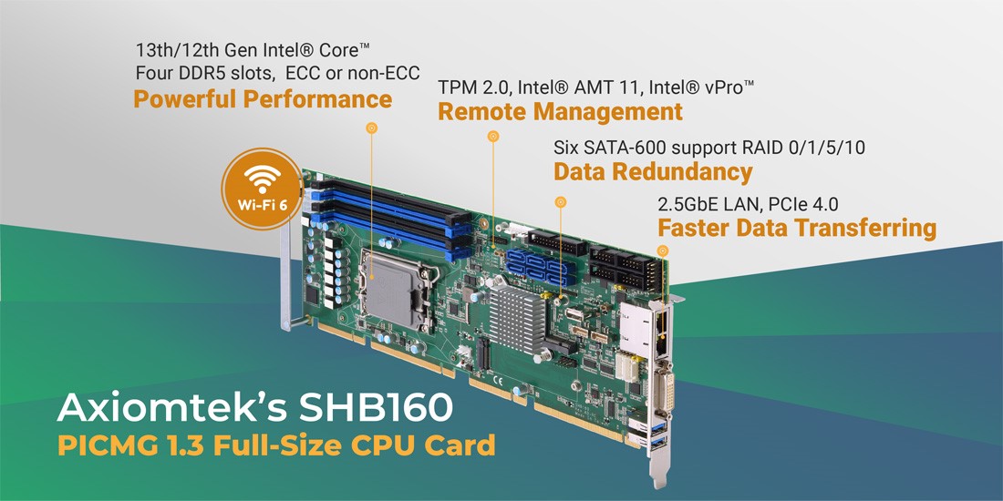
Axiomtek – a world-renowned leader relentlessly devoted to the research, development, and manufacture of series of innovative and reliable industrial computer products of high efficiency – is pleased to announce the SHB160, a new PICMG 1.3 full-size single-board computer powered by the LGA1700 13th/12th Gen Intel® Core™ i7/i5/i3, Pentium® or Celeron® processor with the Intel® R680E/H610E chipset. The industry-specific SBC supports dual 2.5GbE LAN for the ultimate connection experience with blazing data-transfer speed. It also supports PCIe 4.0 for more flexibility and higher bandwidth to GPUs, SSDs, and other peripherals. Offering superior computing performance, rugged design, flexible I/O expansion as well as enhanced graphics capabilities, the SHB160 aims to satisfy the requirements of AIoT applications such as vision inspection, objective classification, factory automation, intelligent video analysis, and smart city.
Advanced Features of SHB160
LGA1700 13th/12th Gen Intel® Core™ i7/i5/i3, Pentium® or Celeron® processor (up to 125W)
Intel® R680E/H610E chipset
DDR5 4400MHz U-DIMM up to 128GB ECC (R680E only)/non-ECC memory
Supports Intel® AMT and vPro (R680E)
Supports RAID 0/1/5/10 (R680E)
TPM 2.0 supported (optional)
Supports dual 2.5GbE
Supports LPT port
Supports M.2 Key M/ Key E (H610E only supports Key E)
Supports PCIe 4.0 through the gold fingers
Axiomtek’s SHB160 offers up to four DDR5-4400MHz ECC or non-ECC U-DIMM slots for up to 128GB of system memory. The full-size slot CPU card has six SATA-600 ports with software RAID 0/1/5/10 support (Intel® R680E chipset) or four SATA-600 ports (Intel® H610E chipset). In addition, the SHB160 has one M.2 Key M 2280 slot with PCIe 4.0 x4 signal for NVMe SSD (Intel® R680E chipset). It also delivers superior graphics performance with the Intel® UHD Graphics and offers dual display configurations via DVI-I and DisplayPort++ (internal header) ports. One PCIe x16 Gen4 slot, one PCIe x4 Gen4 slot or four PCIe x1 Gen4 slots, and four 32-bit PCI bus masters are available on the board to provide an optimum solution with a diverse range of configurations. Equipped with one M.2 Key E 2230 slot, the SHB160 also supports Wi-Fi 6 for faster data transferring while reducing latency and enhancing security.
“To meet the needs of demanding industrial environments, Axiomtek’s single board computer SHB160 is designed with advancing computing efficiency, large memory capacity with maximum four DDR5 slots, and high-speed transferring interfaces for a broad range of intensive computing applications. The SHB160 features optional Trusted Platform Module (TPM) 2.0 for optimum security and supports Intel® Active Management Technology (Intel® AMT) 11 and Intel® vPro™ for easy remote management and monitoring,” said Kasper Tsai, the product manager of AIoT Division at Axiomtek. “In addition, the powerful industrial single board computer supports watchdog timer, hardware monitoring function as well as smart CPU and smart system fans. To ensure reliable operation across platforms, the SHB160 can withstand a wide operating temperature range of 0°C to 60°C.”
Axiomtek’s SHB160 has rich I/O interfaces, including two RS-232, two RS-232/422/485, two 2.5G GbE LAN, two USB 3.2 Gen2x1, four USB 3.2 Gen1x1 (Internal box header), three USB 2.0, four USB 2.0 via golden fingers, one PS/2 keyboard internal connector, and one PS/2 mouse internal connector. The SHB160 is now available for purchase. For more product information or pricing, please visit our global website at www.axiomtek.com or contact one of our sales representatives at info@axiomtek.com.tw.
Exciting Announcement!!! A Brand New Free Functional Testing launched!
With the aim to guarantee superior product quality and enhance customer satisfaction, Seeed Fusion introduced Free Functional Testing Plan two years ago, which garnered tremendous positive responses. Today, we are thrilled to announce a major service upgrade: from now on, Free Functional Testing is available without any limitations on all PCBA orders! You can enjoy this enhanced service with every single PCBA order you place.
PCBA manufacturing is a complex process that involves multiple intricate steps. Consequently, functional testing emerges as a vital quality control method to guarantee optimal performance of the assembled PCB. At Seeed Fusion, we acknowledge the utmost significance of testing. That’s why we are thrilled to announce the official launch of our Free Functional Testing service for all PCBA orders.
Why is testing important?
Nothing is more disappointing than receiving a product dead on arrival, including PCB assemblies. The consequences are costly, both economically and in terms of time, and may be difficult to remedy, especially without the necessary re-work equipment. With small-batch manufacturing, it may not be feasible to utilize more expensive testing methods such as AOI, or x-ray inspection (AXI). That is where functional testing can help.
What is PCBA Functional Testing?
The final quality assurance step in the entire production process, functional testing verifies that the boards do what they are supposed to do, by simulating the real operating environment. This can be as simple as an on/off power test, LED test, or running of a comprehensive software program.
Seeed now provides free functional testing for all PCBA orders to ensure the quality of your PCBA products and avoid costly delays.
As always in manufacturing, the earlier problems are found, the cheaper and easier they are to remedy. By allowing Seeed engineers to take care of testing before the boards are shipped to you, any defective boards can be reworked on-site, ensuring that all boards leaving the production floor work as intended. Our technicians can also perform point-to-point voltage tests, create custom test jigs, and handle burning firmware in-house.
How to Get Free PCBA Functional Testing?
By testing a single piece, you can identify errors that may go unnoticed through visual inspection alone and validate the entire turnkey process. Be among the early adopters to benefit from this service, which is both straightforward and expeditious.
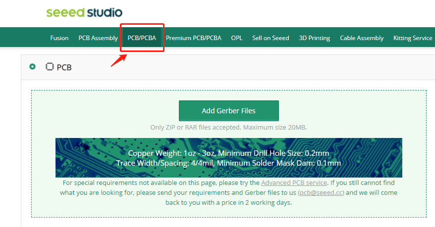
First, as usual, upload your Gerber files and BOM file to Seeed Fusion PCB/PCBA order page, and select the board’s parameters and any other features. The system will generate the PCBA quotation as usual.
After completing the above, navigate to the functional testing section below and select [100% Functional Testing]. Then, upload the test plan instructing us how to test the board functions as expected. You can also upload the test plan before the boards are completed later.
Notes: Functional testing for one piece will typically increase the lead time by around two working days. High precision testing and high voltage testing or any testing that poses a health risk to technicians will not be accepted. Customers will be expected to pay for any specialist tools or materials required for testing.
For more information on our testing procedures and capabilities, please refer to the PCBA functional test FAQ.
With the help of Seeed Fusion functional testing, realize improved yield, greater efficiency, and cheaper turnkey PCB assembly. Get a quotation now and become one of the first to take advantage of free Seeed PCBA functional testing.
Besides free Functional Testing with every PCBA order, Seeed also provides free DFM & DFA reviews to maximize yield and minimize assembly complications.
Seeed has been engaged in the electronic design and production industry for more than 12 years. With extensive manufacturing experience, and ISO9001 quality management standards, Seeed is well aware of the importance of eliminating errors as soon as possible in the production cycle.
That is why, in addition to free PCB Design for Manufacture (DFM) review, we also provide PCBA design for assembly (DFA) review for free with every PCBA order. Now, we are delighted to add free functional testing to our turnkey PCB assembly package. We sincerely hope you will realize the benefits!
If you are very interested in our product but do not want to draw the schematic and layout by yourself for some reason, you are welcome to experience our ODM service. For more information, please contact fusion@seeed.io for help.
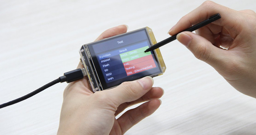
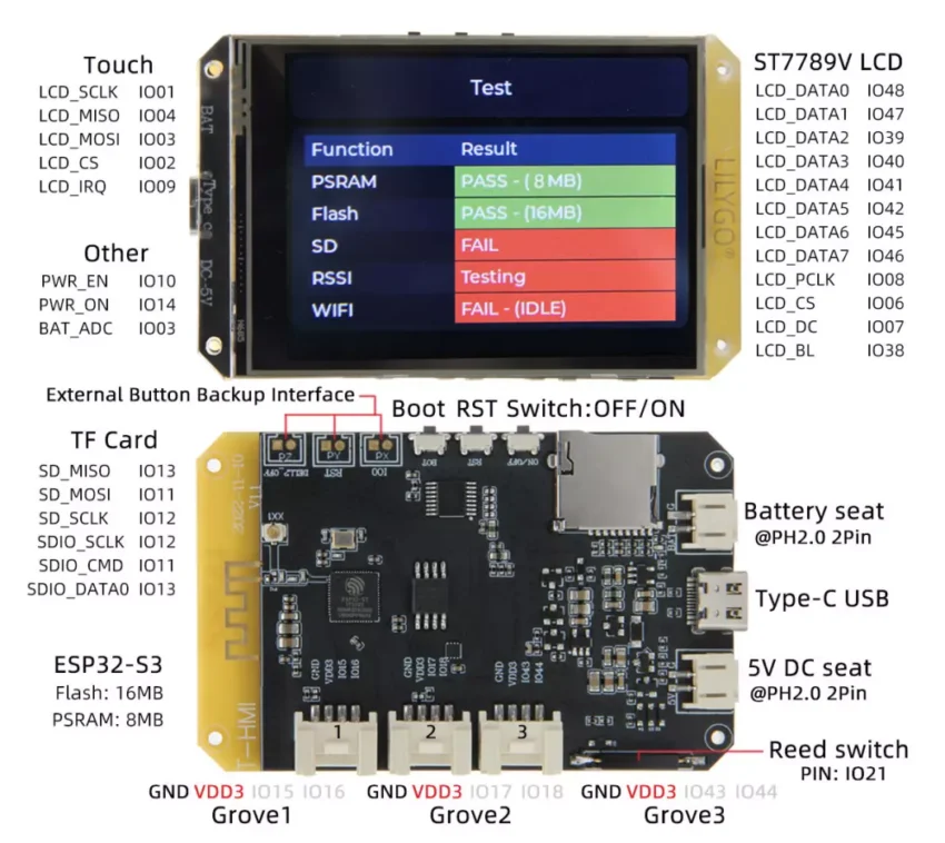
LILYGO, a well-known manufacturer of ESP32-S3 boards, has introduced its latest product, the LILYGO T-HMI board. This board is based on the ESP32-S3 and features a 2.78-inch color display with resistive touch technology, making it an excellent choice for HMI (Human Machine Interfaces) applications. Additionally, the board is equipped with Grove connectors, allowing for easy expansion with sensors or actuators.
Grove connectors are a standardized set of connectors used for rapid prototyping. The system consists of a Base unit, usually a microprocessor, and various Grove modules. The modules can connect to the Base unit to enable different inputs or outputs. Alternatively, if you do not have a Base unit, you can use Grove to Pin Header Converter and connect Grove modules directly to the pins on devices like Raspberry Pi or Arduino.
Regarding support, LILYGO provides a PDF schematic, Example code, Default Firmware, Arduino Library, PlatformIO Library, and a DXF file for reference. All these are available on their official GitHub repo.
Features of the LILYGO T-HMI color display board
The T-HMI is LILYGO’s touch display screen with an ESP32-S3 chip. The screen uses a 2.8-inch ST7789 LCD and is equipped with a resistive screen stylus/pen; more features are listed below,
wireless MCU – ESP32-S3 with dual-core Tensilica LX7 running up to 240 MHz
16MB SPI flash, 512KB RAM, 8MB PSRAM, and microSD card socket for expanded storage.
Connectivity – 2.4 GHz Wi-Fi 4 (802.11 b/g/n) with 40 MHz channel support, BLE 5.0 with long-range capabilities
Antenna – PCB antenna and external u.FL antenna support.
Display – 2.8-inch 320×240 color (RGB) display with resistive touch support
USB – USB Type-C port for power and programming.
Expansion – 3 Grove connectors for expansion modules.
Power Supply – 5V via USB Type-C port or 2-pin JST PH2.0 connector, support for LiPo battery.
Dimensions – Compact dimensions of 80 x 50 x 12.5mm.
One tiny problem with this board is that the USB port used for JTAG requires the CDC_ON_BOOT configuration to be enabled. If that is disabled or the port cannot be found during program upload, you must manually enter the upload mode by pressing and holding the BOOT button while connecting the USB and then clicking reset on the programming software.
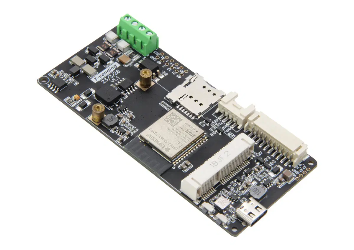
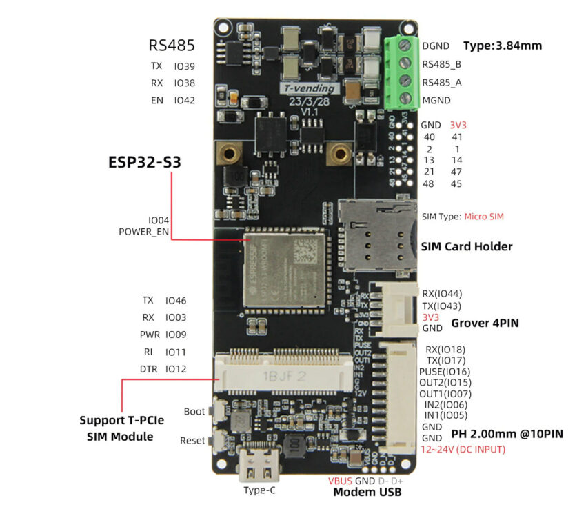
Undoubtedly, the ESP32 has become one of the most popular development platforms over the years. That is why the developer’s community has used this microcontroller to build many cool boards like UNIT DualMCU, Banana Pi Centi, M5Stack CoreS3, Seeed Studio XIAO, and many more. But what piqued our interest is the LILYGO T-Vending Board, a vending machine board developed on top of ESP32-S3, and it has support for RS485, 4G connectivity, and even an SD card to log data.
The LILYGO board is designed to be connected to the vending machine through the RS485 terminal block, so this board will act as the master board driving a slave motor controller board to run the machine. Additionally, there is a 10-pin connector to power the coin mechanism and other parts. The board incorporates a Grove connector and includes an unpopulated 12-pin GPIO header, allowing further expansion and customization.
Adding a sim card to the LILYGO T-Vending Module
To use 4G cellular functionality you need to install a T-PCIe module such as the SIM7600 model, but doing so completely covers the ESP32-S3 module with its antenna so it’s unclear what effects it might have with the WiFi and Bluetooth signals.
In terms of support, LILYGO provides a PDF schematic and some example code like Factory, Modem_ATDebug, RS485_Master, RS485_Slave, SPIExample, and WireExample showing how to use I2C. all this is available on their official GitHub repo.
One major drawback of this board is that this board doesn’t come with a complete example project. So, if you plan to use this board in your project, you’ll have to figure out the integration part and write the program from scratch. It’s a bit hard to do, but it’s possible to make this work with some quality time with the coding.
Features of LILYGO T-Vending Board
This little board comes packed with features, so we have listed those in the section below,
Dual-core Tensilica LX7 microcontroller with up to 240 MHz clock speed
2.4 GHz 802.11n WiFi 4 and Bluetooth 5.0 LE connectivity with ESP32-S3
8MB PSRAM and 16MB SPI flash memory
PCB antenna for wireless communication
MicroSD card slot data storage
RS485 A/B terminal block for serial communication
USB Type-C port for programming and a 4-pin header for Modem USB 2.0 interface
A 4-pin Grove connector (UART), a 12-pin GPIO header, and a 10-pin connector for UART, PULSE, GPIOs, and DC input
Reset and Boot buttons for convenience
Powered by a 12-24V DC supply via a 10-pin connector
Compact dimensions of 102 x 46 x 12.5mm.
You can buy the T-Vending board from LILYGO on Aliexpress for a price of $25.72, and that includes free shipping! If you’re in need of cellular connectivity, you can opt for one of their T-PCIe modules like the SIM7600 series. The price of this ranges from $36 to $51, depending on where you’re at. So, you’ve got options to deck out your board and get it up and running without breaking the bank!
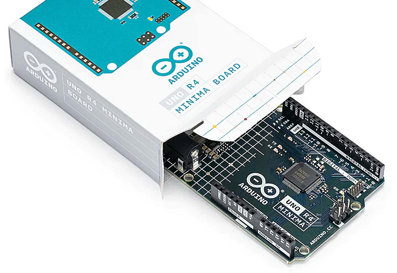
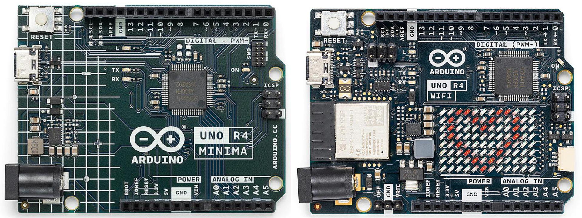
The Arduino Uno has been the “go-to” board for beginners for its simplicity and versatility as it makes a great choice for professionals to develop a proof of concept for their target use cases. Continuing the legacy, Arduino has recently announced the Arduino Uno R4 Minima and R4 Wi-Fi, the successor to the Arduino Uno R3.
While the R4 Minima is a generational upgrade to the R3’s overall power and features, the R4 Wi-Fi adds the features of Wi-Fi communication and a matrix display to the R4 Minima for IoT application implementation.
Technical Specifications of the R4 and R4 Wi-Fi
The 32-bit RA4M1 microprocessor, 32 kB of quicker RAM, and 256 kB of faster Flash memory are all included in the Arduino Uno R4 Minima. The R4 Minima keeps the same amount of PWM-enabled digital I/O pins and analog input pins.
Additionally, the R4 Minima includes a 12-bit DAC, CAN Bus, and an OP-AMP, which are upgrades for customers seeking greater adaptability in the same R3-compatible design. The inclusion of the CAN Bus is particularly beneficial for Internet of Things applications since it permits connecting to other devices in the network – without a host device.
Through the barrel jack connector, the R4 Minima improves the power specifications of its predecessor by supporting a voltage range of 6V to 24V. The seamless connectivity of relatively high-power equipment like motors, LED strips, etc. is made possible thanks to this. In order to continue working with older devices, the R4 Minima core’s operating voltage is 5V. Additionally, Arduino has added the traditional 5V and 3.3V power connectors for compatibility and relevant applications.
R4 Wi-Fi Adds More to the R4 Minima
Using the ESP32-S3, which operates at 240 MHz and 3.3 V, the R4 Wi-Fi combines all the functionality of the R4 Minima, and it adds many more features. With a separate 384 KB of ROM and 512 KB of SRAM, this microcontroller equips the R4 Minima with Wi-Fi, Bluetooth, and BLE networking features.
The ESP32-S3 microcontroller provides AI acceleration through vector calculation instructions, making the R4 Wi-Fi a reliable AIoT device if these characteristics weren’t enough. Moreover, the inclusion of the 12 x 8 matrix display is a key addition to the utility of the IoT functions enabled by the R4 Wi-Fi.
Software and IoT Integration of Arduino Uno R4
The Arduino family of devices has become a solid platform for the development of projects because of its IDE features and easy-to-use programming language.
With the addition of the SWD debugging port, native support for the Qwiic ecosystem of devices, HID device support, and wireless connectivity, the R4 Wi-Fi aims to amplify the abilities of the platform and become a universal option for microcontroller-based projects for beginners and professionals alike. Additionally, the AI-accelerated vector instructions help in the execution of repeated tasks much faster than normal processing to reduce latency and give a much more responsive human interaction experience.
Despite developing such a formidable platform for IoT, Arduino has attempted to take things further by announcing an online API service named Arduino IoT Cloud. The service enables users to code, visualize, monitor, and debug IoT-connected Arduino devices remotely and without achieving much expertise in wireless communication systems and protocols.
On a conclusive note, Arduino has a very strong portfolio of microcontrollers. The addition of processing power, IoT support and various other features to the R4 Minima and R4 Wi-Fi give Arduino a wider sense of appeal as a universal platform for beginners and professionals alike.
The Arduino Uno R4 Minima and R4 Wi-Fi are on sale for $20.oo and $27.50, respectively. For more information, visit the official product pages of Uno R4 Minima and Uno R4 Wi-Fi.
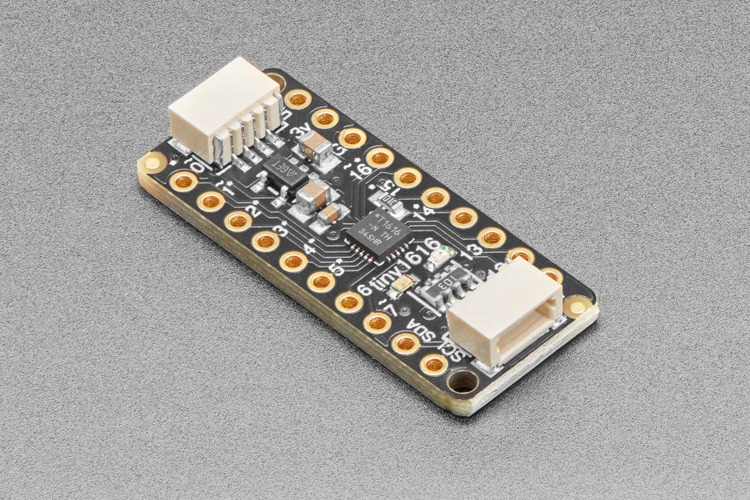
Adafruit’s latest ATtiny1616-basedbreakoutboard is slightly more unique than the average breakout board you can commonly find in the market. Not only this board features the SeesawFirmware, but it also features the STEMMAQT/ Qwiic connector, through which you can use this board as a plug-and-play I2C controller or peripheral.
So, why would you need a separate microcontroller as an I2C peripheral? Does the main microcontroller already have all the necessary functionality? Well, it all depends on the project requirements. Sometimes, you may need additional GPIOs; sometimes, there could be a need for extra ADC. In other cases, there could be a situation where strict timing requirements need to meet for a peripheral to work.
When discussing strict timing requirements, the WS2812B is a great example. The LEDs will only light up if the timing is managed correctly. Speaking of Neopixel, this board is perfect for driving Neopixel LEDs because it has a dedicated Neopixel driver capable of driving up to 250 LEDs.
So, having an I2C expansion board on top of your microcontroller is cool and all, but doesn’t make the coding part more complicated? Well, it turns out that Adafrut is also taking care of that by giving us custom software libraries for Arduino and Python which is the two most used embedded development platforms.
The seesaw firmware runs on a microcontroller, like Microchip’s ATtiny1616 breakout board, and handles all the communication processes, the ATtiny1616 comes preloaded with the seesaw firmware and you have custom libraries available for Arduino and Python. The code is pretty simple, here is an example code for setting up PWM on the ATTiny1616 breakout board:
# SPDX-FileCopyrightText: 2021 ladyada for Adafruit Industries
# SPDX-License-Identifier: MIT

# Simple seesaw test for writing PWM outputs
# On the SAMD09 breakout these are pins 5, 6, and 7
# On the ATtiny8x7 breakout these are pins 0, 1, 9, 12, 13
#
# See the seesaw Learn Guide for wiring details.
# For SAMD09:
# https://learn.adafruit.com/adafruit-seesaw-atsamd09-breakout?view=all#circuitpython-wiring-and-test
# For ATtiny8x7:
# https://learn.adafruit.com/adafruit-attiny817-seesaw/pwmout

import time
import board
from adafruit_seesaw import seesaw, pwmout

i2c = board.I2C()  # uses board.SCL and board.SDA
# i2c = board.STEMMA_I2C()  # For using the built-in STEMMA QT connector on a microcontroller
ss = seesaw.Seesaw(i2c)

PWM_PIN = 12  # If desired, change to any valid PWM output!
led = pwmout.PWMOut(ss, PWM_PIN)

delay = 0.01
while True:
    # The API PWM range is 0 to 65535, but we increment by 256 since our
    # resolution is often only 8 bits underneath
    for cycle in range(0, 65535, 256):  #
        led.duty_cycle = cycle
        time.sleep(delay)
    for cycle in range(65534, 0, -256):
        led.duty_cycle = cycle
        time.sleep(delay)
The example code is taken from Adafruit’s website and you can check that out for more information.
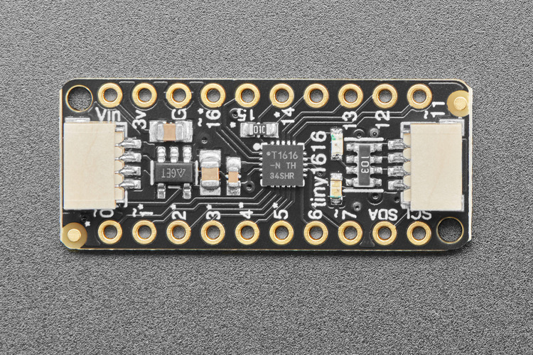
The Adafruit ATtiny1616 breakout is interesting because it uses Microchip’s new family of microcontrollers the ATtiny1616. Despite its compact size, it offers 16 kilobytes of flash memory, 2 kilobytes of RAM, and 256 bytes of program-accessible EEPROM. Furthermore, it features an internal oscillator clocked at 20 MHz.
By default, the breakout board operates at 5V, but the operating voltage range of the ATtiny1616 microcontroller is between 2V to 5V. That is why there is a 3.3v regulator onboard; the regulator provides flexibility allowing seamless interfacing with 3.3V devices.
Features of the Adafruit ATtiny1616 Breakout Board
The ATtiny1616 breakout board from Adafruit offers many features designed to extend the capabilities of microcontrollers. Here are the key specifications:
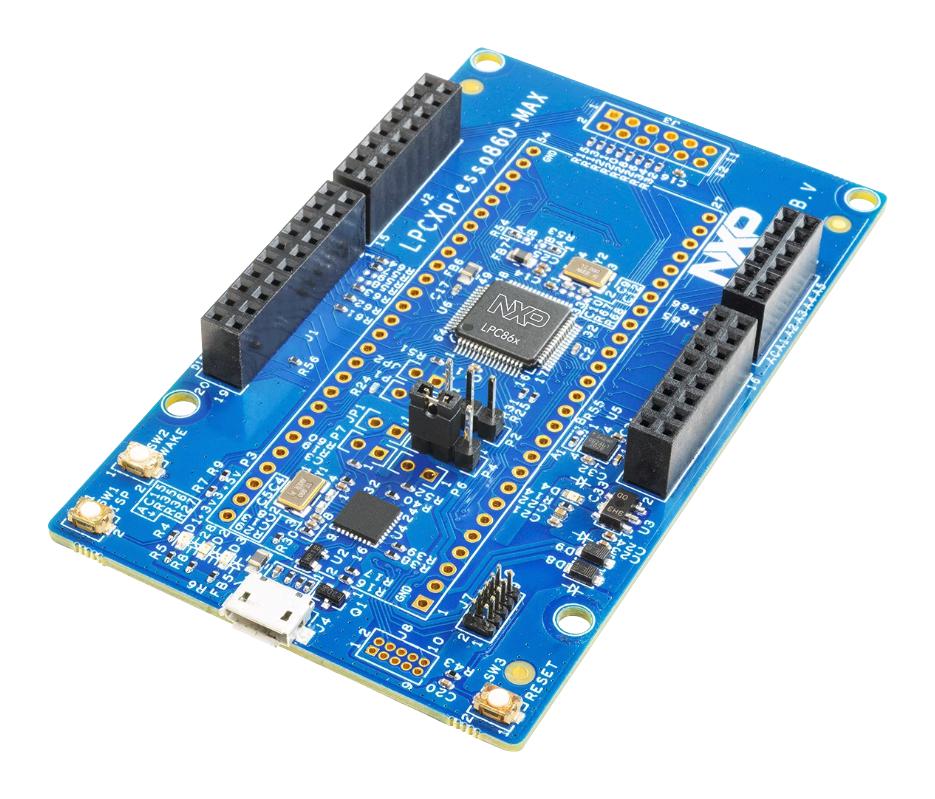
NXP, a leading semiconductor manufacturer, has recently announced its new evaluation board with the LPC86x processor. This evaluation board features the LPC860-MAX chip, which includes a 32-bit ultra-low-power Arm Cortex-M0 processor which has 54 GPIO pins. With a net cost of $15, this board supports a range of moderate to lightweight applications such as Battery Management Systems(BMS), Building Safety, Motor Drives, Smart Lighting, Smart Speakers, and more.
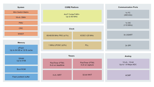
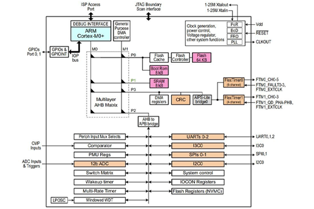
This new development board features the LPC860-max at its core. With a maximum clock speed of 60MHz, the Cortex-M0 processor offers impressive processing capabilities and a fast single-cycle I/O port. Additionally, this processor provides 64kB of Flash memory and 8kB of RAM, ensuring sufficient storage and computational power for a wide range of applications.
Specifications of the NXP LPC860-MAX Microcontroller
32-bit Arm Cortex-M0+ processor with 60MHz Clock
Single-cycle multiplier and fast single-cycle I/O port
6-channel FlexTimer with motor fault control
4-channel FlexTimer with quadrature encoder
64kB flash memory with 8kB RAM
Windowed Watchdog Timer (WWDT)
Self-Wake-up Timer (SWT)
1x comparator with 5 inputs and internal/external reference voltage
1x DMA with 16 channels and 13 trigger inputs
1x 12-bit ADC (Analog-to-Digital converter)
3x USART , 2x SPI and 1x I2C
1x I3C port (a mid-speed alternative to SPI and compatible with I2C)
Supported by NXP’s software and tools
Compatible with Keil MDK IAR EWARM development environments
Equipped with up to 54x GPIOs (General Purpose Input/Output pins)
Looking at connectivity, this evaluation board offers a wide range of options. It includes a Comparator with five inputs and support for internal/external reference voltages. The board also features a 16-channel DMA with13 trigger inputs, which further enhances its data transfer capabilities. other than that it has, a 12-bit ADC, 3 USART, 2 SPI, 1 I2C, and 1 I3C (>10MHz) providing developers with multiple communication interfaces to suit their specific requirements.
To simplify the development process, NXP support for the LPC860-MAX evaluation board through its MCUXpresso Software and Tools. These software development tools offer a development environment for programming Kinetis, LPC, and i. MX RTmicrocontrollers. The MCUXpresso SDK also provides project files for Keil,MDK, and IAR EWARM, offering flexibility to developers who prefer these development environments.
With NXP’s commitment to providing innovative solutions for the embedded systems market, the LPC860-MAX evaluation board empowers developers to unlock new possibilities and deliver cutting-edge products to consumers across various industries.
In the previous parts of the article, we considered how to convert an analog signal to digital by PCM method, as a binary encoding process. Now we want to consider the reverse process as binary decoding. This combination of binary encoding/decoding procedures is an essential part of signal processing in thousands of applications in the industry and the world of technology.
The purpose of digital-to-analog conversion is to take discrete numerical data (which represent an analog signal) as the input and reproduce the original continuous waveform as the output. Digital-to-analog converters (DACs) are used in transforming digital processing data, back to ‘real-world’ values for further analog processing.
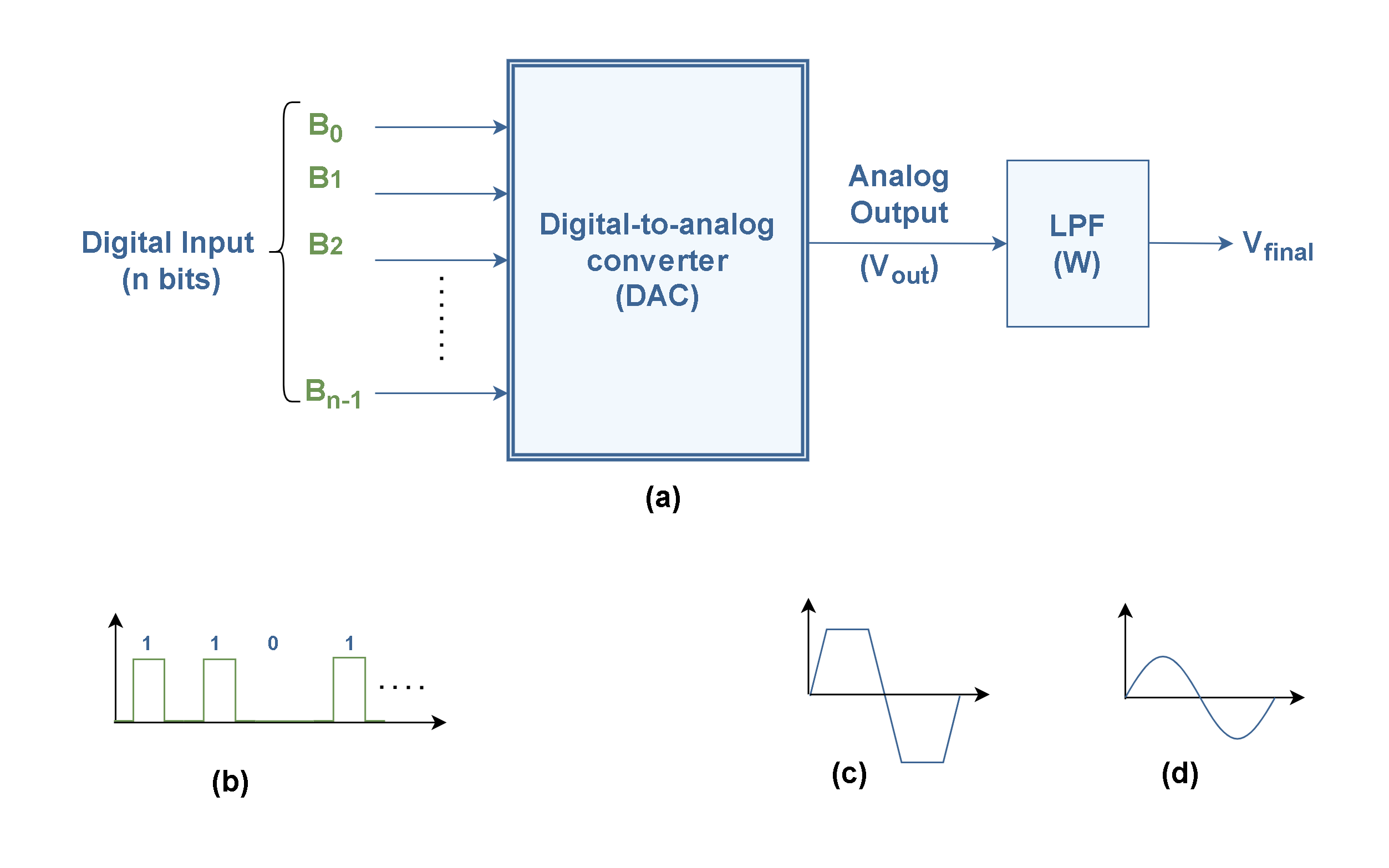
Digital-to-analog converters actually perform the role of re-constructing the original continuous electrical waveform. Since DACs in their configuration are much simpler than ADCs (analog-to-digital converters), they are correspondingly cheaper. Figure 1 shows the schematic of an n-bit DAC.
Figure 1: (a) An n-bit DAC with an LPF after the output terminal (b) Digital waveform at the input (c) Unfiltered analog waveform at the output (Vout) (d) Filtered analog waveform (Vfinal)
Figure 1 (a) shows the main function of an n-bit DAC system to convert binary words [Bn-1 … B1B0] to analog signals at the output (Vout). The typical input waveform is plotted in Figure 1 (b). Although the output analog signals are usually not perfectly reconstructed, as it shown in the typical waveform in Figure 1 (c), a low pass filter (LPF) is almost always necessary to correct the final waveform to be more similar to the original, as shown in Figure 1 (d).
Reconstruction Of The Original Continuous Signal
There are many applications that require the construction of analog waveforms from the digital sequence of numbers. The most common digital-to-analog converter is multiplying DACs. The name arises because the output is constructed by summation of the products of the binary code values and voltage sources. Each bit of the binary code turns on or off a corresponding voltage source. The sum of all the available voltages produces a resultant voltage for output.
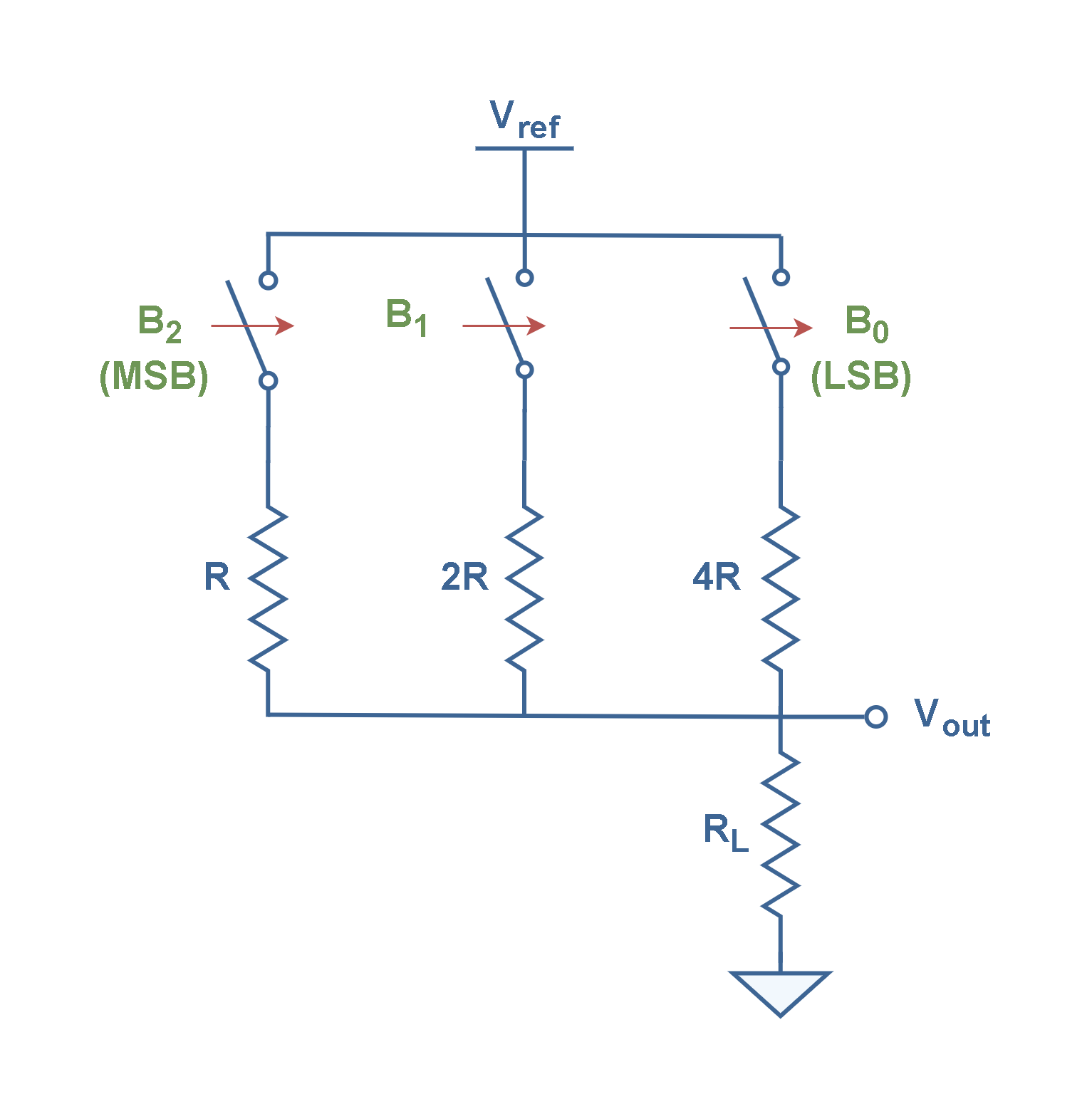
For this purpose, simple resistive networks can be used. Figure 2 shows the concept of converting a three-bit digital input into an analog output by such a resistive network. The resistors are scaled specifically to represent weights for the different input bits. The bits are assumed as electronic switches which may close the circuit while their values are ‘1’ and may also open branches while their values are ‘0’.
Figure 2: Weighted resistive circuit for 3-bit digital to analog conversion
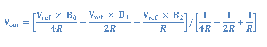
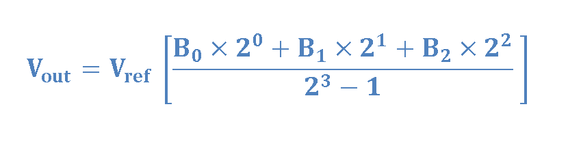
Figure 2 shows the network with a main voltage source (Vref) and three voltage dividers. With the help of simple circuit analysis, like Millman’s theorem, it can be proved that the output voltage is given by Equation 1.
Equation 1: Calculation of the output voltage for the 3-bit weighted resistive DAC
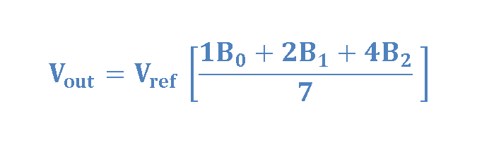
In this expression, B0, B1, and B2 are numerical values of input bits which may be 0 or 1. This expression can be simplified to Equation 2.
Equation 2: The output voltage of the 3-bit weighted resistive circuit
It can be further expressed by considering the weight of bits as Equation 3.
Equation 3: The output voltage of the 3-bit weighted resistive circuit
Thus, Vout is a voltage waveform as the counterpart of the digital word of [B2 B1 B0] at the time of exiting this word (T).
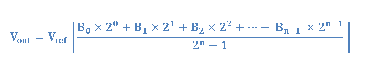
The configuration in Figure 2 can be extended to an n-bit weighted resistive D/A converter to get the following generalized expression in Equation 4.
Equation 4: Generalized calculation of the output voltage for an n-bit weighted resistive DAC circuit
According to Equation 4, a logic ‘1’ at LSB (the least significant bit) position (B0) would contribute Vref /(2n −1) to the output voltage. The contributions of successive higher bit positions in the case of a logic ‘1’ would be 4Vref /(2n −1), 8Vref /(2n −1), and so on. Finally, a logic ‘1’ in MSB (the most significant bit) position would deliver (2n-1. Vref )/(2n −1) to the output, as the most contribution.
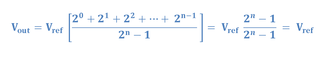
When all input bit positions have a logic ‘1’, the maximum analog output is given by Equation 5.
Equation 5: Maximum value of Vout for the n-bit weighted resistive circuit
In the case of all inputs being in the logic ‘0’ state, Vout = 0. Therefore, the analog output Vout of the resistive DAC varies from 0 to Vref volts as the digital input varies from an all 0s to an all 1s input. Equation 6 explains the range of the output amplitude Vout .
Equation 6: The minimum and maximum ranges of Vout
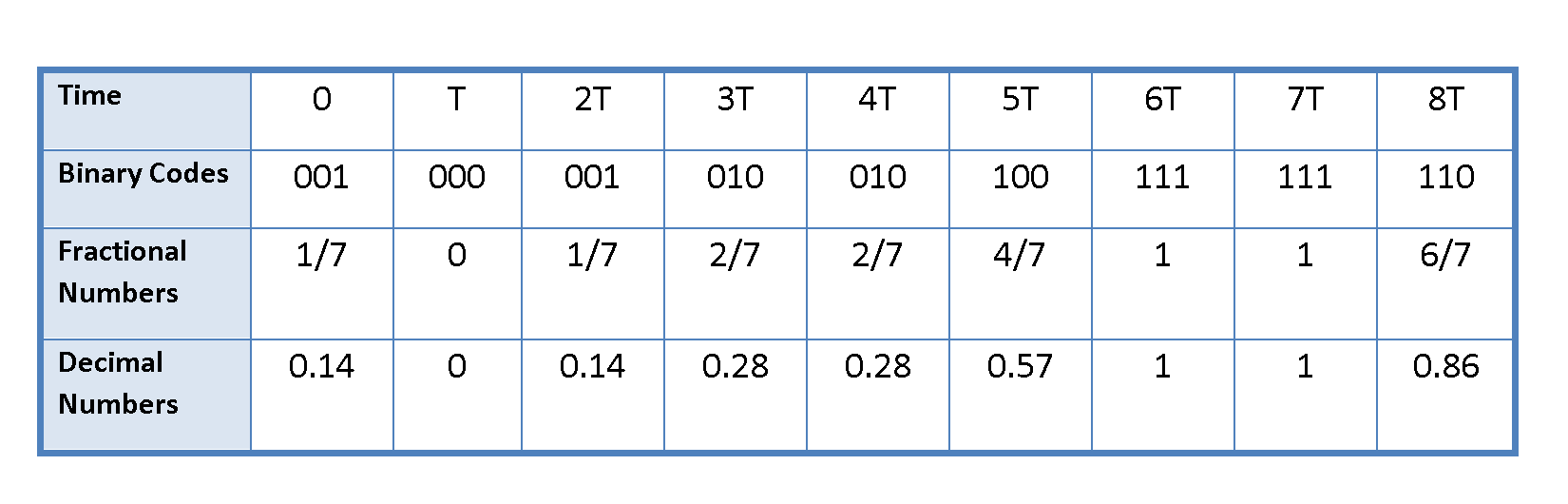
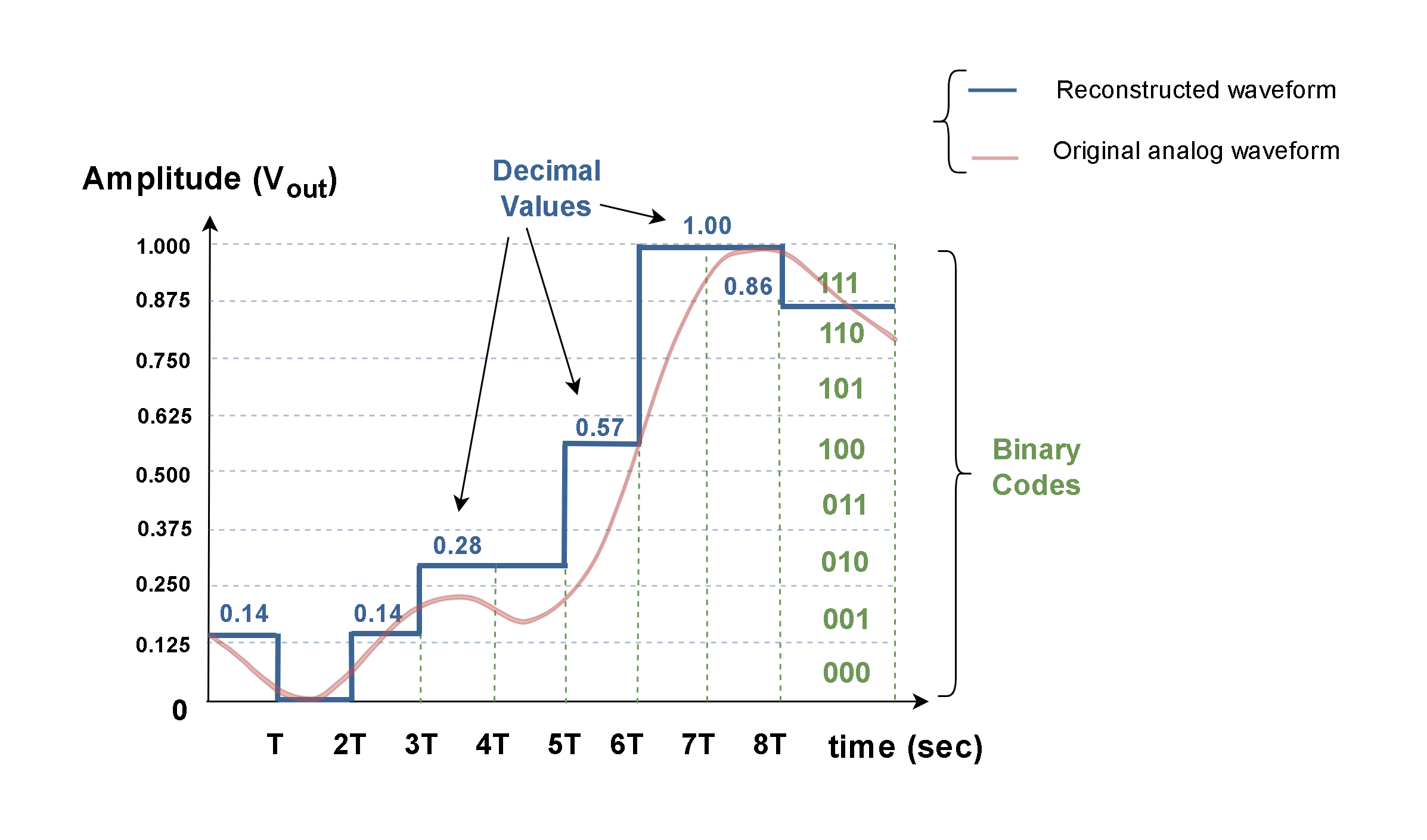
Let’s recall our previous example in the second part of the article:
If we take the results of the ADC conversion in that example as our new input binary data and apply the weighted resistive D/A converter to that binary numbers, the new decimal values result in Table 1 (Vref = 1 V).
Table 1: The decimal output results of DAC corresponding to the digital codes from the previous example
If we plot the results of Table 1 in terms of time, the original analog waveform is reconstructed approximately as shown in Figure 3.
Figure 3: Reconstructed analog waveform by the 3-bit weighted resistive DAC
Obviously, this approximation of the original waveform is not perfect! As we have already considered, the precise conversion of analog waveforms to digital (or from digital domain to analog) needs a large number of bits (3-bit words are normally not enough). A better approximation will be achieved by increasing the number of bits (n).
Also, this waveform is before the stage of filtering. To achieve a smoother curve, an LPF is applied after the output in practical DAC systems.
Weighted-Resistor Network For D/A Conversion
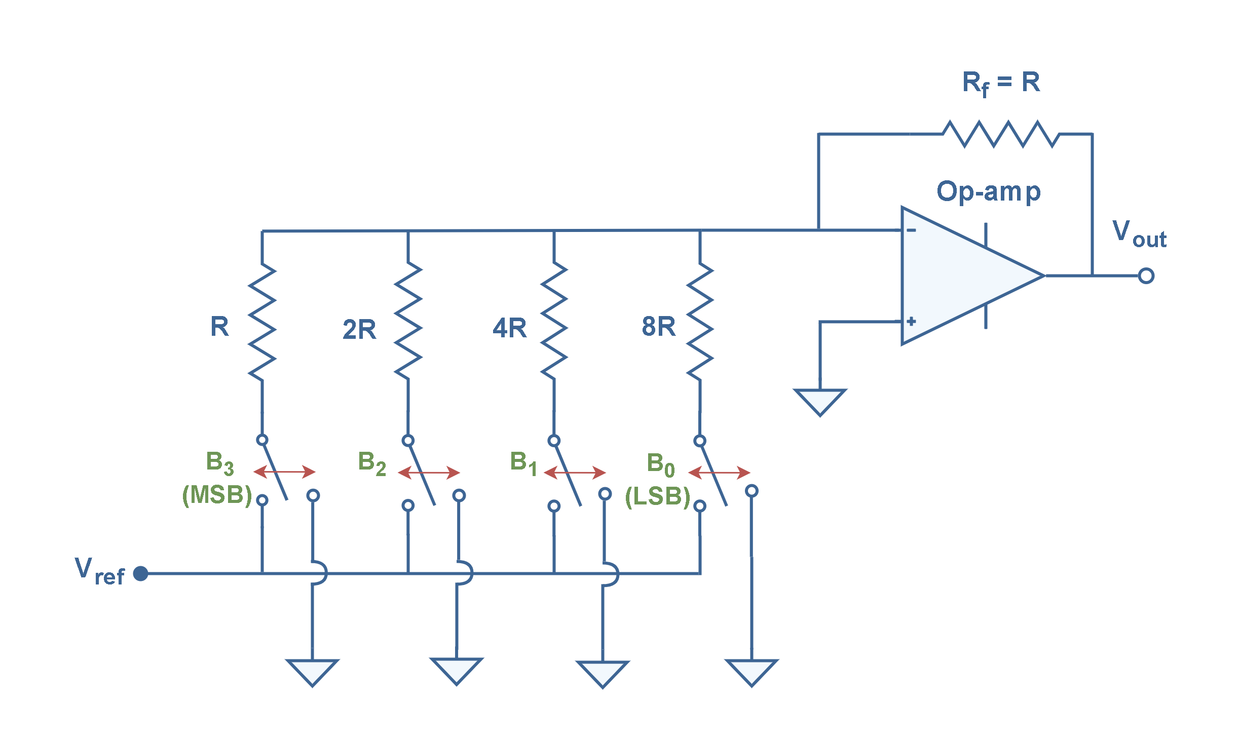
Based on the prior resistive DAC concept, Figure 4 shows a more realistic configuration for a DAC circuit utilizing an operational amplifier.
Figure 4: A 4-bit weighted resistive DAC with a summing amplifier
Essentially, this configuration is a weighted-resistor decoder that converts a 4-bit code from digital to analog. The values of resistors are chosen such that the resistance in each branch is double the previous one, i.e. the current reduces by a factor of 2 for each branch or bit path. This arrangement confirms a proper conversion from a binary number to a decimal value. The overall circuit simultaneously uses the ideas of a summing amplifier and an inverting amplifier, with the output voltage Vout.
The voltage source (Vref), as the reference of logic ‘1’ or ‘on’, is applied to a series of scaled resistors. The voltages at one end of the resistors are either switched ‘on’ or ‘off’ relating to the status of input bits as shown in Figure 4. The ‘off’ voltages are grounded to zero and the ‘on’ voltages are summed. The output is proportional to the weighted sum of the input voltages.
The resistor with the lowest value R corresponds to the highest weighted binary input B3 (MSB) with a weight of 23 (= 8). The other resistors with values of 2R, 4R, and 8R respectively correspond to the binary weights of 22 (B2) and 21 (B1), and 20 (B0 which is LSB).
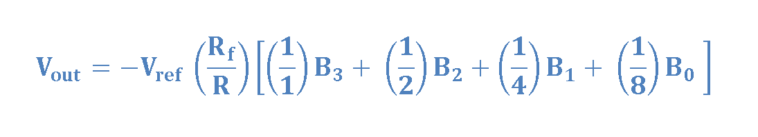
The relationship between the digital input sequence [B3 B2 B1 B0] and the analog output Vout is as Equation 7.
Equation 7: Calculation of Vout for a 4-bit DAC Converter with a summing amplifier
If Vref is originally selected by negative polarity, the positive Vout will be achieved. Some DAC devices have a built-in reference voltage source. Other ones allow the user to provide an external reference voltage, thereby setting the accuracy of the output.
Binary Ladder Network For D/A Conversion
The simple resistive decoder concept of Figure 2 has two serious practical disadvantages:
Each resistor in this network has a different value. Specifically, there is a large difference in resistor values between the LSB and MSB for a large number of bits (n). Such networks usually use precision resistors. Precision resistors are designed for applications where fitted resistance tolerance and stability are primary considerations. Therefore, such a configuration causes extra expenses.
The resistor used for the most significant bit (MSB) is required to handle a much larger current than the LSB resistor. So, for a larger number of bits, we need a set of resistors with different sizes and current characteristics.
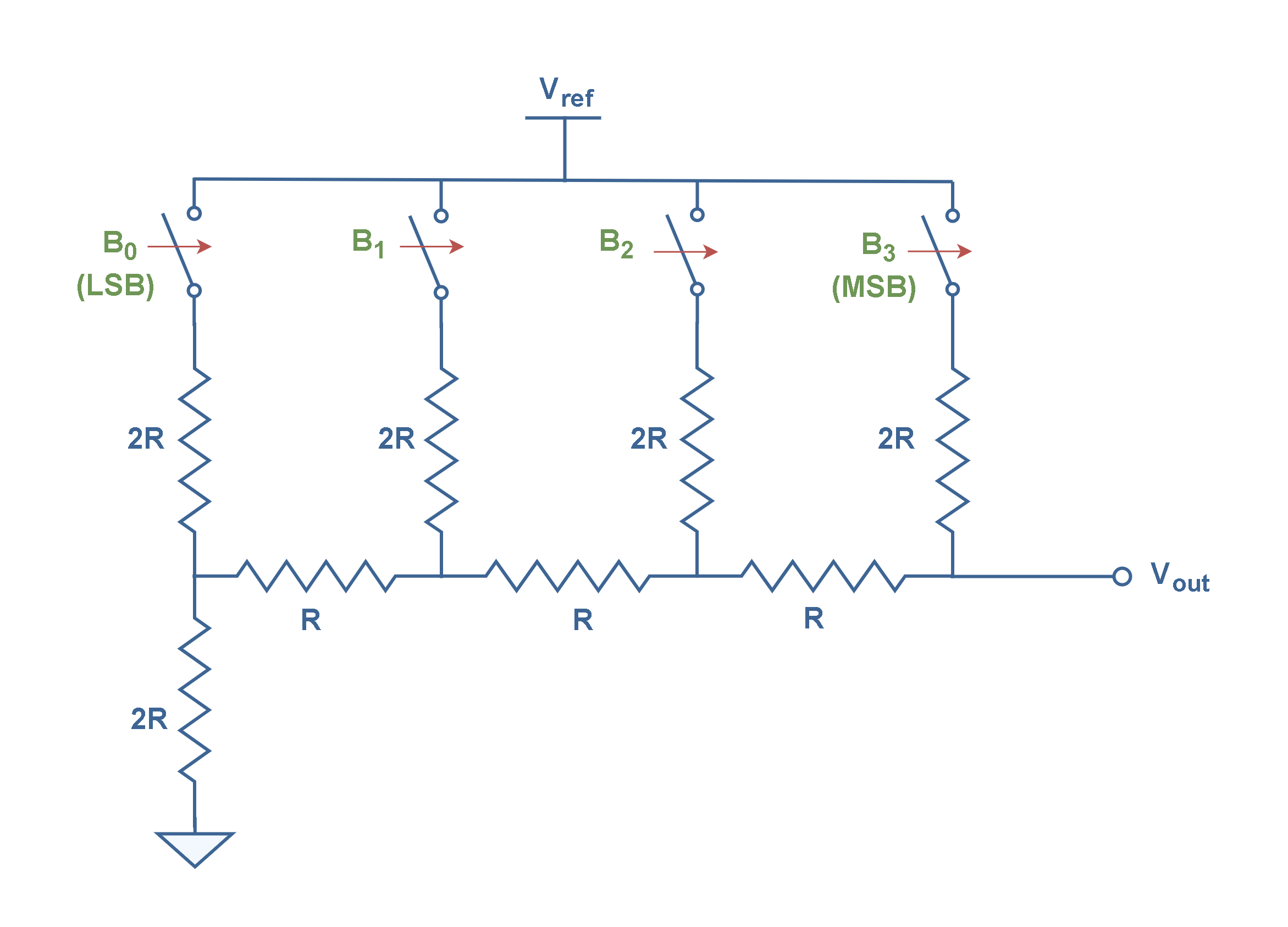
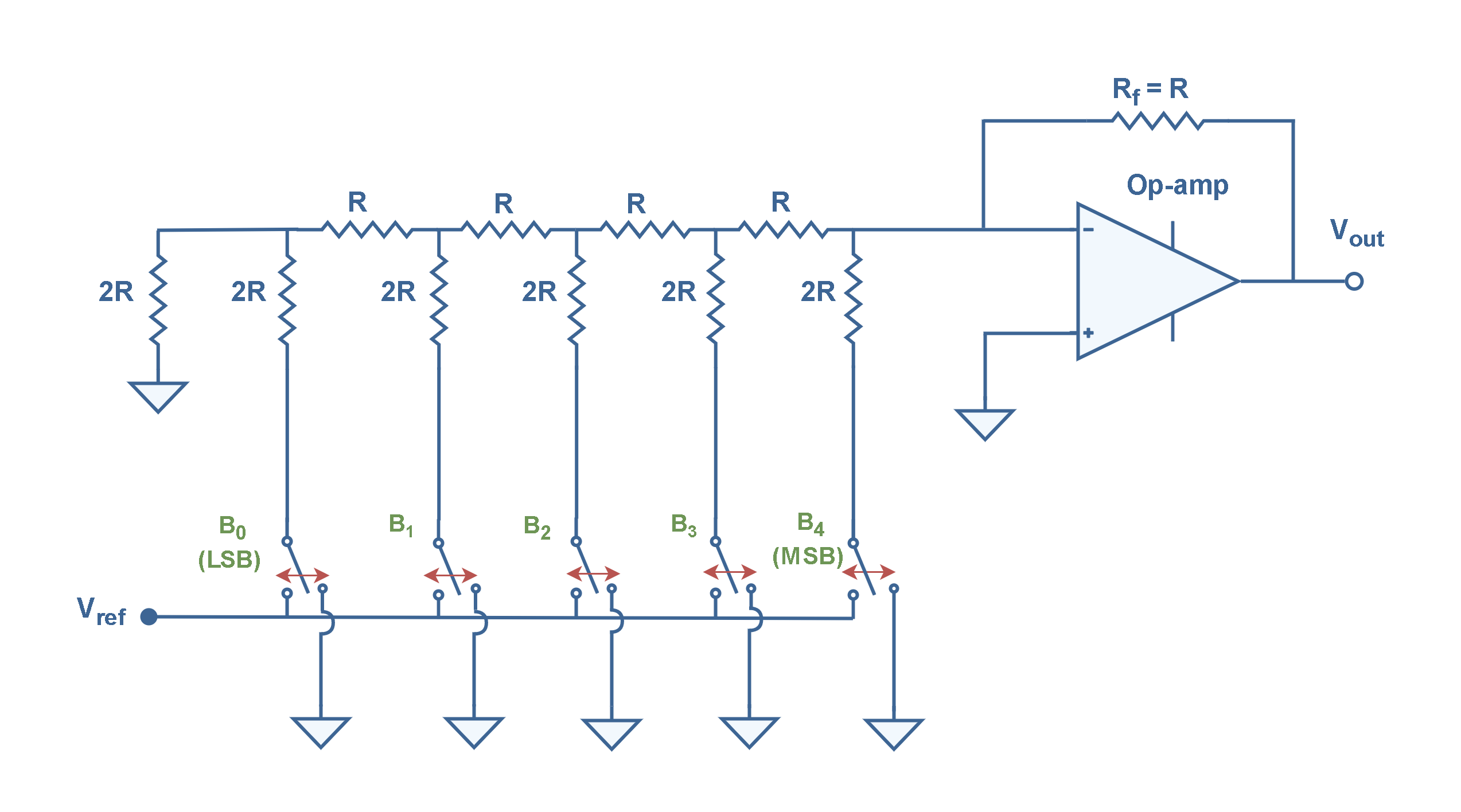
To overcome these disadvantages, a second type of resistive network called the binary ladder (or R/2R ladder) is used in practice. The binary ladder is also a resistive network that produces an analog output equal to the weighted sum of digital inputs. Here the resistance values span a range of only 2 to 1.
Figure 5 describes the concept of the basic R/2R binary ladder network for a four-bit D/A converter.
Figure 5: R/2R binary ladder resistive circuit for digital-to-analog conversion
The “ladder” description comes from the ladder-like topology of the network. This configuration operates as an array of voltage dividers whose output accuracy is exclusively dependent on how well each resistor is matched to the others.
Note that the network consists of only two resistor values; R and 2R (twice the value of R) no matter how many bits make up the ladder. For this reason, the R/2R ladder is inexpensive and relatively easy to manufacture. All bits pass through resistance of 2R. The less weighty the bit, the more resistors the signal must pass through before reaching the output.
The digital inputs or bits range from LSB (B0) to MSB (B3). The bits are switched between 0 Volt and Vref and each binary input adds its own weighted contribution to the analog output Vout depending on the state and position of the bit. The MSB causes the greatest effect in output voltage and the LSB causes the smallest.
By methodical application of Thevenin’s Equivalent circuits and Superposition Principle, it is possible to analyze the R-2R circuit. With the help of simple mathematics, it can be proved that the analog output voltage Vout in the case of binary ladder network of Figure 5 is given by Equation 8.
Equation 8: Analog output voltage of the binary ladder network (R/2R)
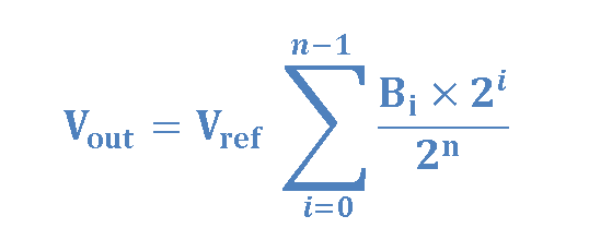
This configuration is easily extendable. Equation 9 explains how to calculate the analog output voltage Vout for a ladder network with n bits.
Equation 9: Calculation of Vout for an n-bit R/2R binary (R/2R) ladder
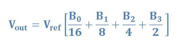
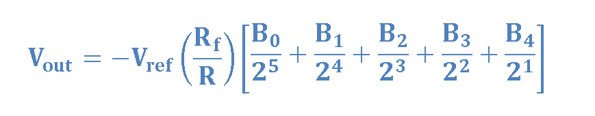
Figure 6 shows a more practical implementation of the R/2R resistor ladder network as a digital-to-analog converter using an op-amp as an inverting summing amplifier.
Figure 6: A 5-bit R/2R DAC with an op-amp summing amplifier
This type of DAC is also known as a multiplying converter. The output voltage is linearly proportional to the digital input states and the range can be adjusted by changing the reference voltage Vref. The Thevenin resistance of an R/2R ladder is always R –regardless of the number of bits in the ladder. Therefore, in this configuration, the source impedance as seen by the op-amp is always constant and equal to R.
The output voltage is the result of Equation 10.
Equation 10: Calculation of Vout for a 5-bit R/2R DAC with op-amp summing amplifier
A binary ladder R/2R network is the most widely used network for digital-to-analog conversion for obvious reasons:
Easily scalable to any desired number of bits
Uses only two values of resistors which makes for easy and accurate fabrication and integration
Having a fixed output impedance of the ladder (R) simplifies filtering and further analog signal processing and circuit design
The R/2R network provides an accurate method of digital-to-analog conversion.
Such D/A converters of different sizes (eight-bit, 12-bit, 16-bit, etc.) are available in the form of monolithicintegrated circuits.
Summary
A digital-to-analog converter (DAC) takes digital data at its input and converts them into analog voltage or current that is proportional to the weighted sum of digital inputs.
Digital codes are typically converted to analog voltages by assigning a voltage weight to each bit in the digital code. This function can be done by a simple resistive network.
By summing the voltage weights of the entire code, the analog voltage is reconstructed.
The most popular networks are the binary-weighted resistive and the R/2R ladder.
Both circuits will convert digital voltage information to analog, but the R/2R ladder has become the most popular due to the network’s inherent accuracy superiority, and ease of manufacture.
The R/2R ladder is made up of only two different values of the resistor. This overcomes one of the drawbacks of using precision resistors in the weighted resistive network.
The R/2R ladder networks provide a simple, inexpensive way to perform digital-to-analog conversion.