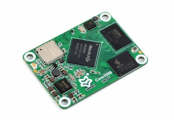
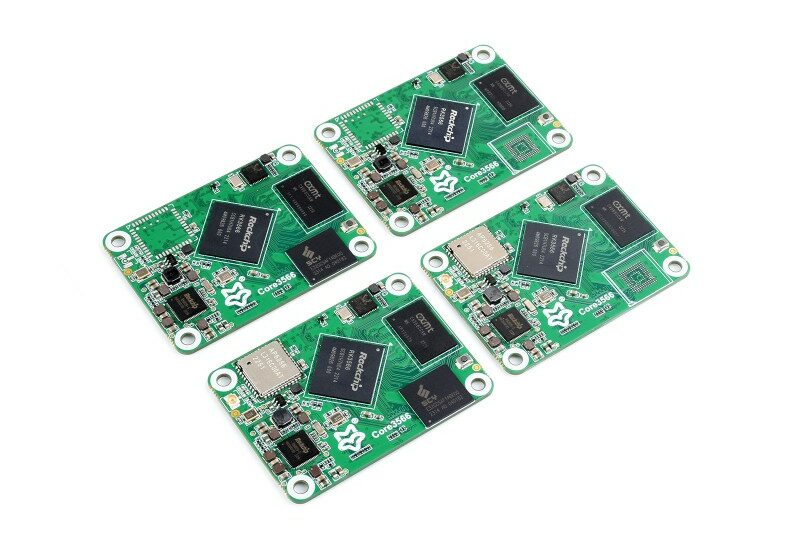
The LuckFox Core3566 Module is designed to become a compelling alternative to the widely popular Raspberry Pi Compute Module 4 (CM4), offering compatibility with CM4 baseboards while delivering powerful performance and advanced features. Designed to cater to the needs of developers, hobbyists, and enthusiasts, this module boasts a range of capabilities, making it a good option for advanced visual applications.
At the heart of the LuckFox Core3566 Module is the Rockchip RK3566 system-on-a-chip (SoC). This quad-core Cortex-A55 processor has a clock speed of up to 1.8 GHz, ensuring efficient execution of tasks. Additionally, the SoC incorporates a 32-bit RISC-V MCU, enhancing its compatibility with various applications.
Complementing its processing power, the Arm Mali-G52 GPU, supporting OpenGL ES 1.1/2.0/3.2, OpenCL 2.0, and Vulkan 1.1, ensures advanced graphics performance. Moreover, the integrated NPU (Neural Processing Unit) provides AI acceleration capabilities, offering a performance of 0.8 TOPS (Trillions of Operations Per Second). NPU supports one-click switching of mainstream frameworks such as Caffe and TensorFlow. The one-click switching capability allows users to easily switch between AI frameworks based on their specific project requirements and preferences.
The LuckFox Core3566 Module comes with advanced wireless connectivity options. Equipped with dual-band Wi-Fi and Bluetooth AP6256 module, users can experience high-speed internet access and seamless Bluetooth connectivity. With dual-band Wi-Fi, this module enables users to surf the web from anywhere, offering increased flexibility and convenience. It is important to note that the Wi-Fi function is optional, and the module requires an additional antenna for the Wi-Fi module as it does not feature an onboard antenna.
The LuckFox Core3566 Module also has an integrated VPU (Video Processing Unit). The VPU is designed to handle demanding video encoding and decoding tasks, ensuring high-quality video playback and efficient video processing. The Core3566 Module’s VPU supports 4K resolution at 60 frames per second and offers hardware decoding for popular video codecs such as H.265, H.264, and VP9.
The LuckFox Core3566 Module is available for purchase, starting at $23.99 for the 2GB RAM variant without flash storage and wireless connectivity.
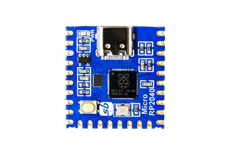
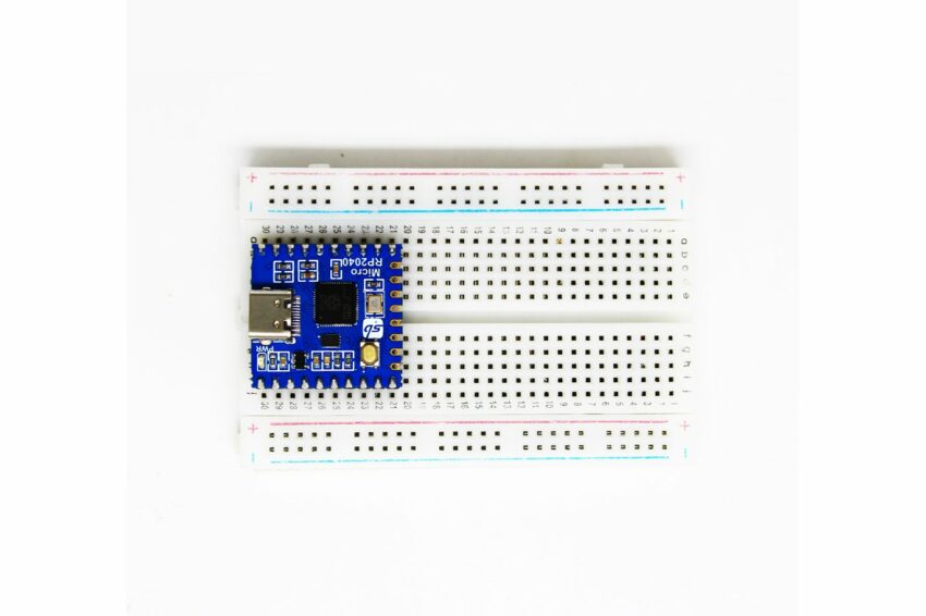
The Micro RP2040 microcontroller board is a powerful development tool that includes most of the features of the Raspberry Pi Pico in a smaller and more compact form factor. The board is designed for hobbyists, students, and professionals, for a wide range of projects, from building robots and controlling smart home devices to experimenting with electronics.
Inside the Micro RP2040 is the RP2040 MCU, a dual-core Arm Cortex M0+ processor. With a clock speed of up to 133 MHz, this microcontroller can handle demanding tasks while keeping power consumption to a minimum. The RP2040 MCU also features a variety of built-in peripherals and interfaces, including USB, SPI, I2C, and UART, providing seamless connectivity options for your projects. You can find more detailed technical information about the RP2040 MCU in the datasheet available here.
Interestingly, the Micro RP2040 has 23 multifunction GPIO pins, which provide sufficient options for connecting sensors, displays, and other peripherals. These pins can be easily programmed to suit your specific project requirements, offering flexibility and expandability. Additionally, the board comes equipped with a USB Type-C connector, enabling straightforward connections to a computer or power source, making it incredibly convenient to use.
Specifications of Micro RP2040 microcontroller board:
Microcontroller: Raspberry Pi RP2040 featuring dual-core Arm Cortex-M0+ processor, clocked at a frequency of 133 MHz
Memory: 264kB of SRAM
Storage: 2MB QSPI flash
Interfaces: 23x multifunction GPIO pins
Serial communication: PWM, I2C, SPI, and UART
Power: USB Type-C port for the power source of 5V
Button: Boot button can be used to enter bootloader mode when the board is powered on
Software: C, C++, and MicroPython
Dimensions: 25 x 24.95 mm
Weight: Approximately 4 grams
When it comes to software support, the Micro RP2040 has you covered. It offers compatibility with a wide range of programming languages and development environments, ensuring that you can work with the tools you’re most comfortable with. Whether you prefer C, C++, or MicroPython, you can unleash your creativity and bring your ideas to life with ease.
The Micro RP2040 microcontroller board is available for purchase at an affordable price of $6.99 on Tindie, making it accessible to enthusiasts and professionals alike. With its compact size, powerful performance, and extensive connectivity options, it allows the user to explore the capabilities of RP2040 to create innovative IoT projects.
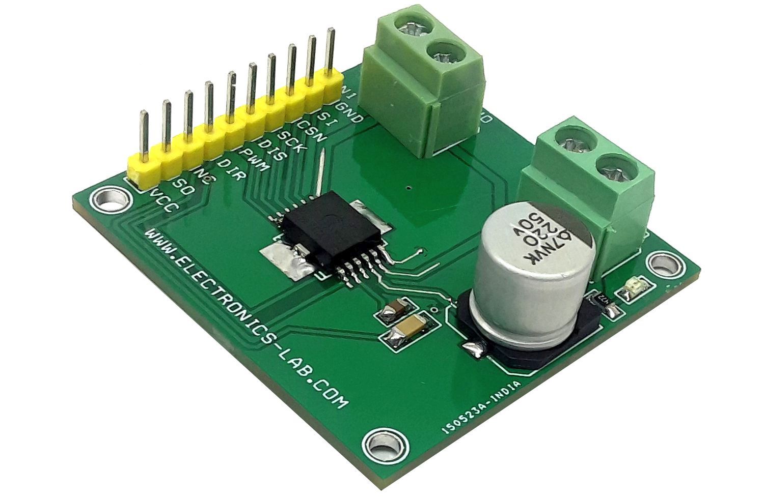
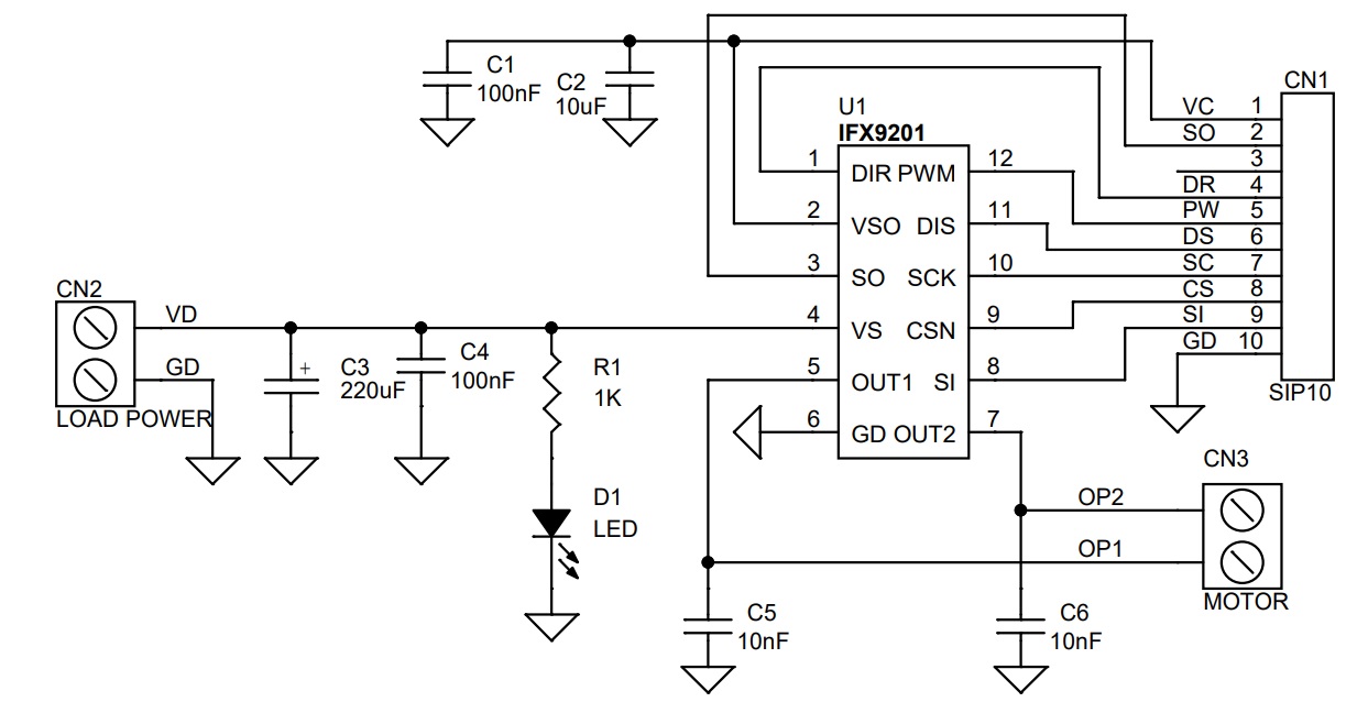
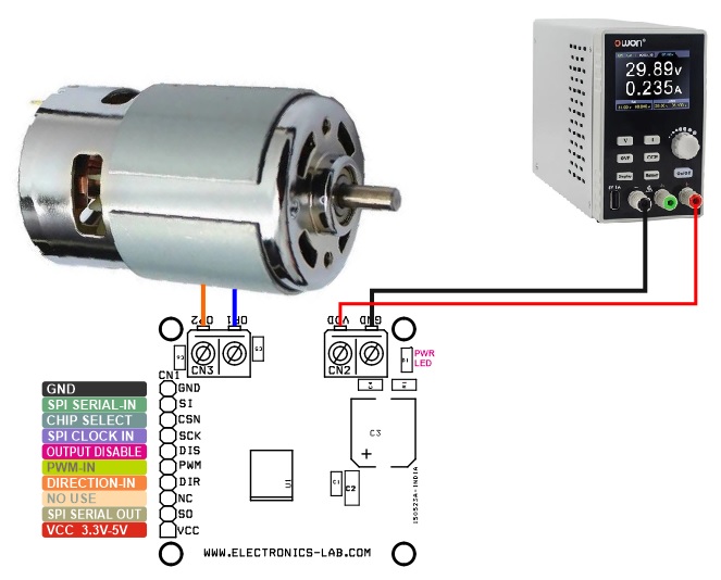
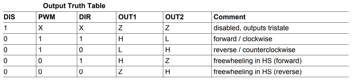
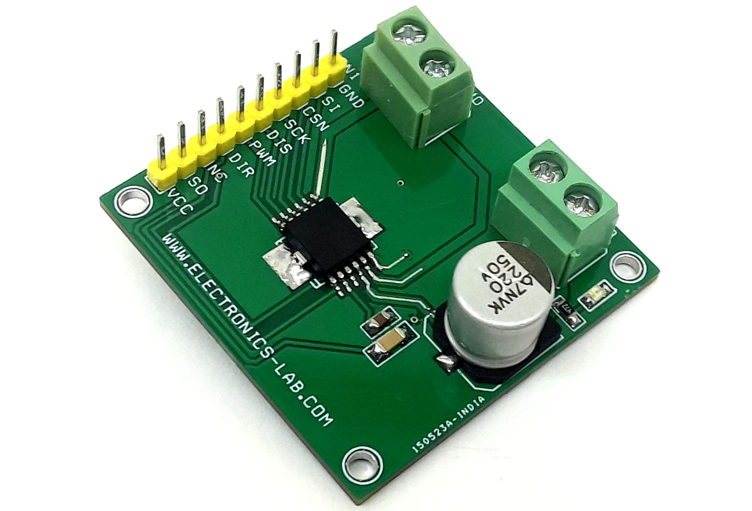
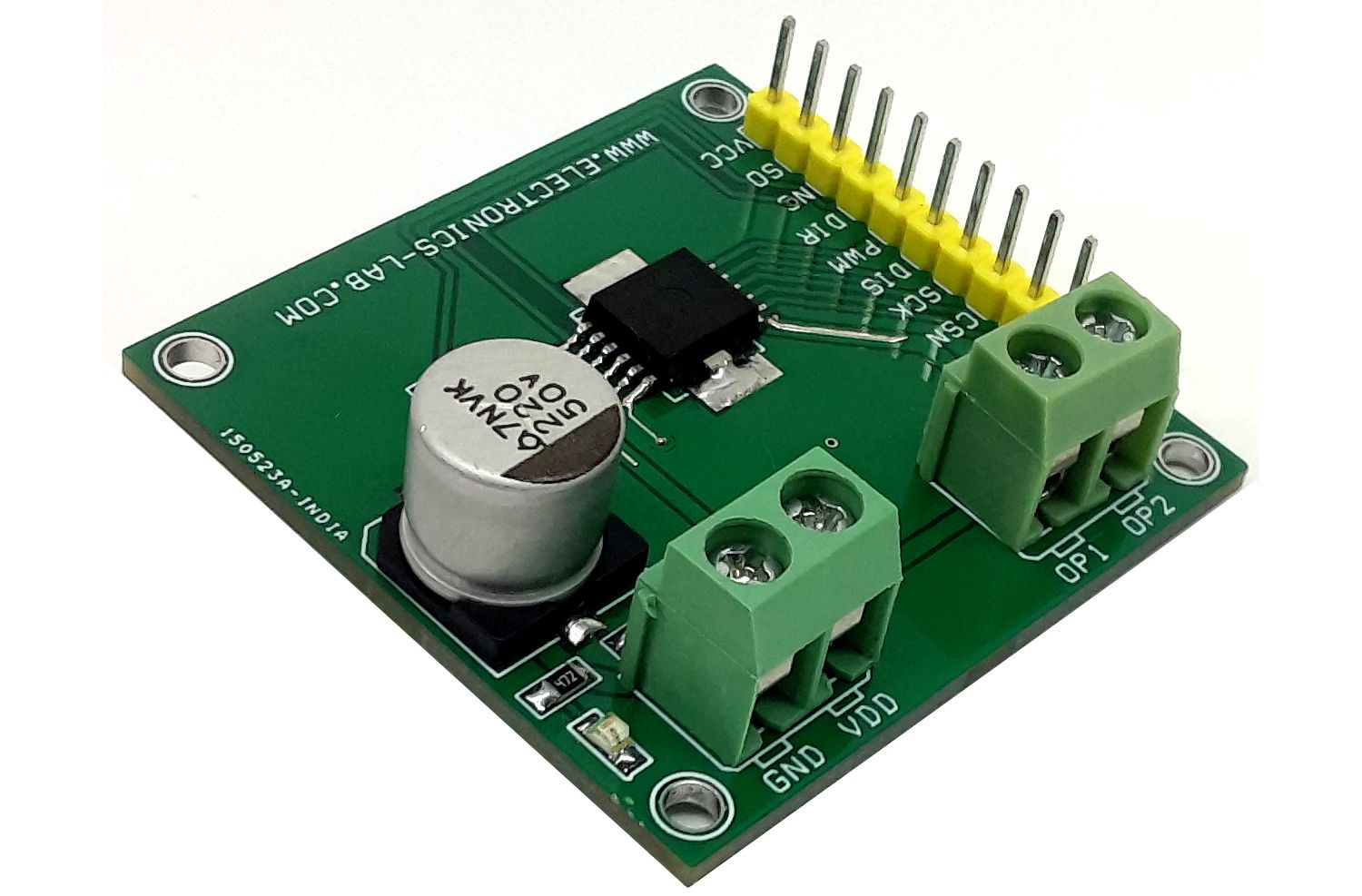
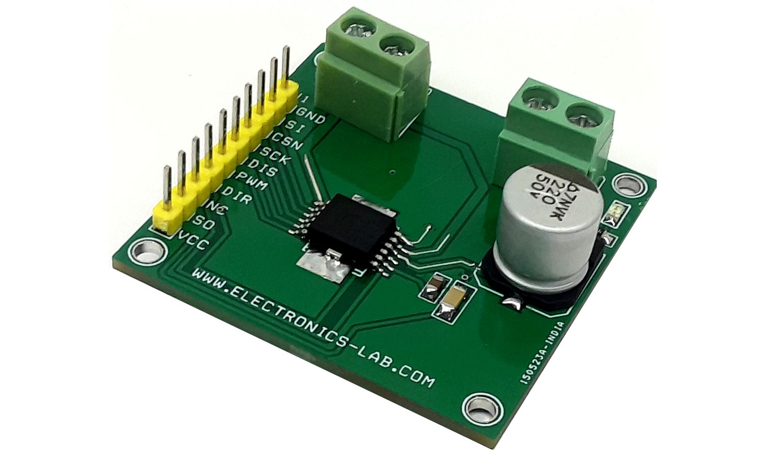
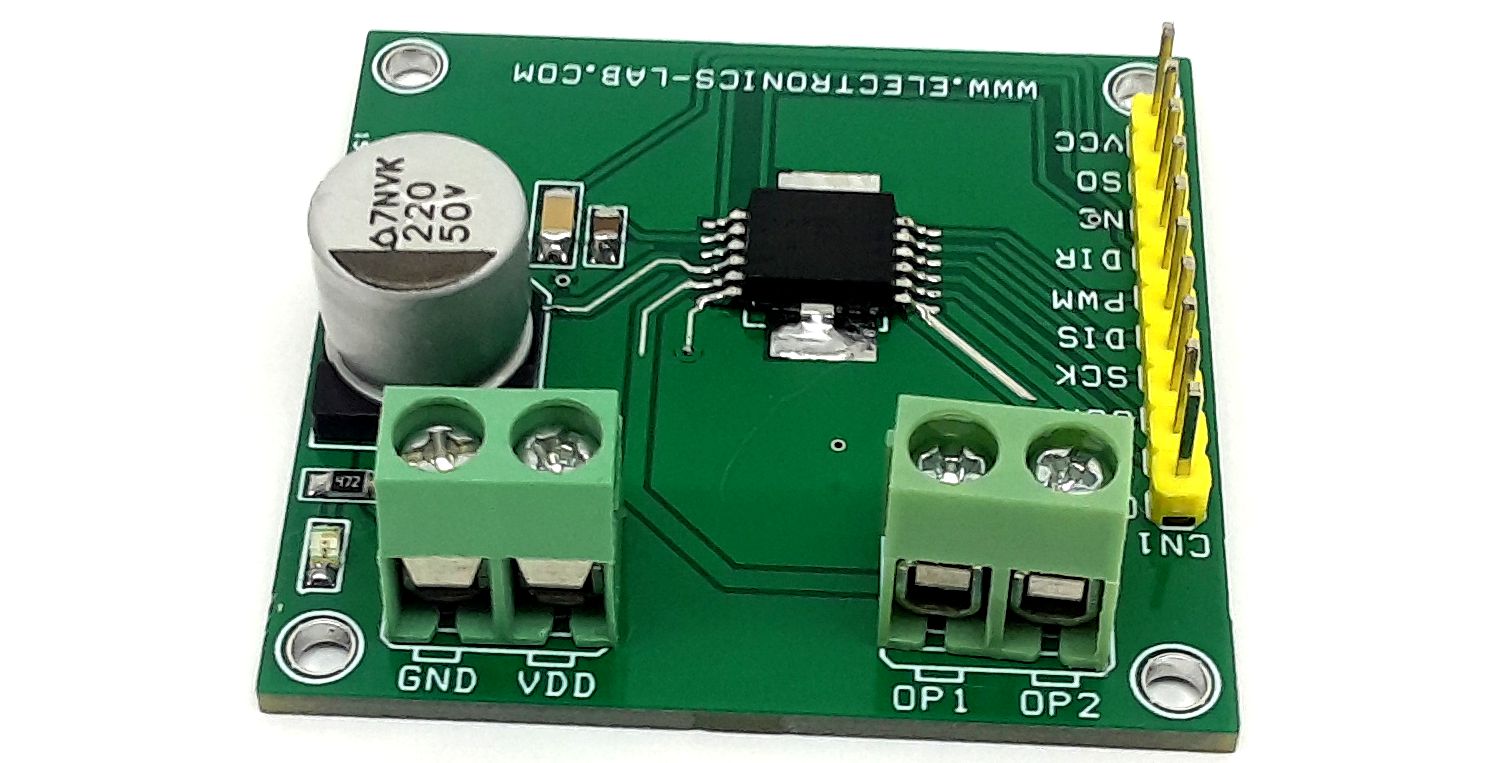
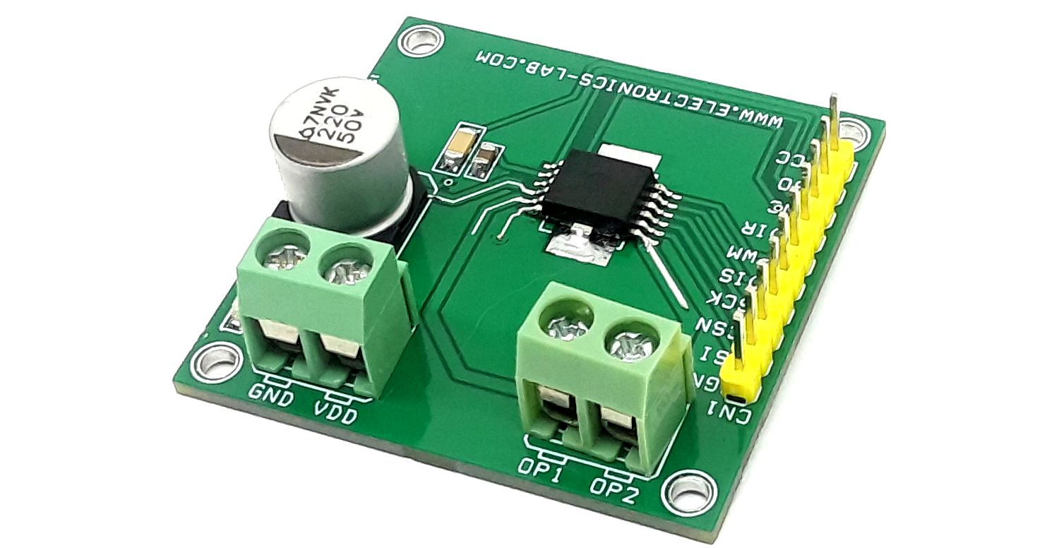
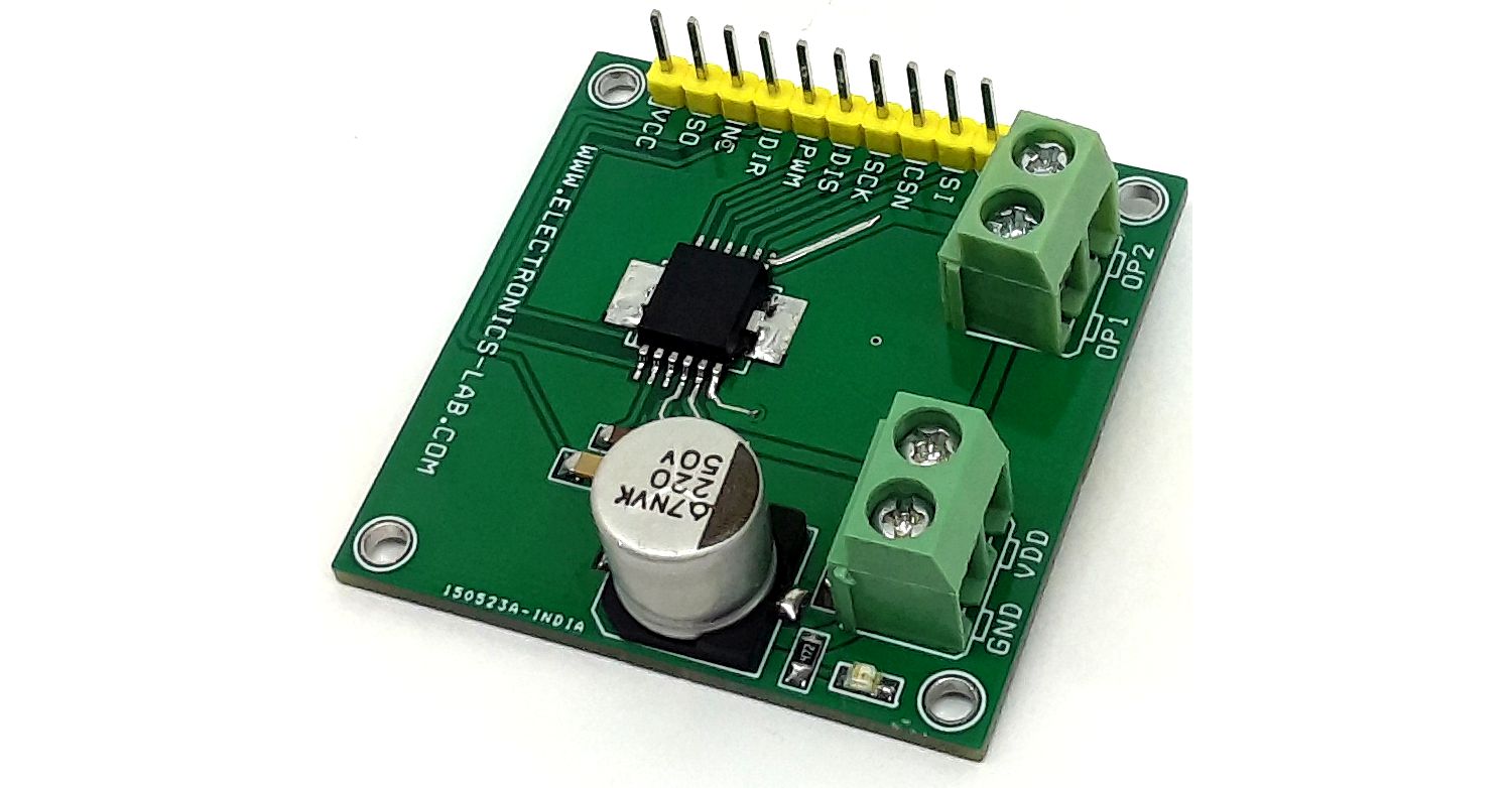
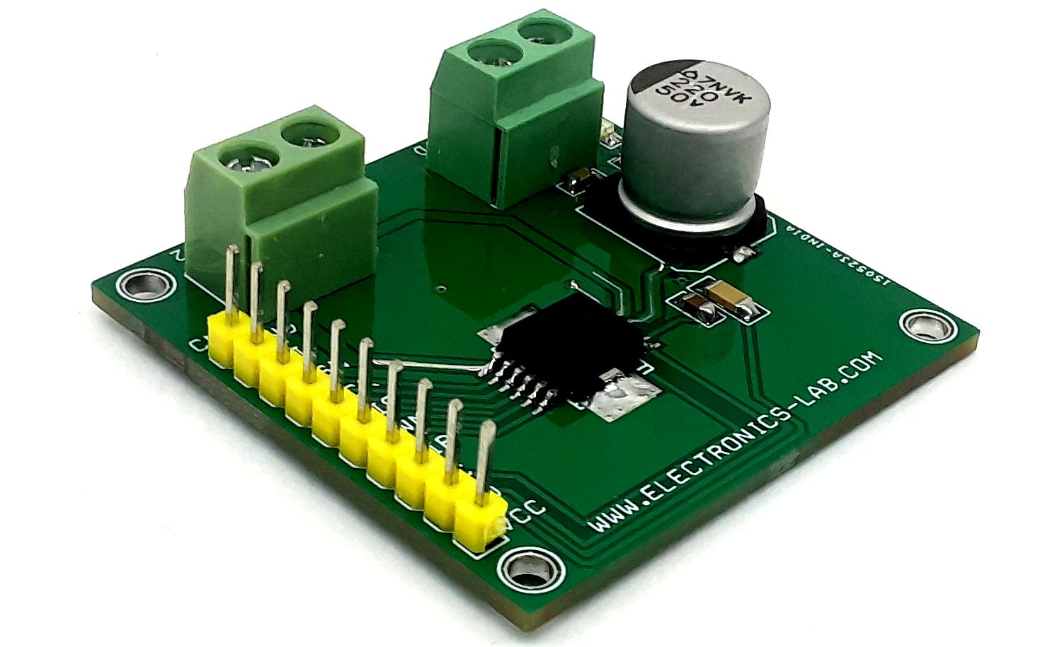
This 6A H-Bridge is designed for the control of DC motors or other inductive loads. The outputs can be pulse width modulated at frequencies up to 20kHz. PWM/DIR control reduces the number of PWM-capable pins needed on the microcontroller side. For load currents above the current limitation threshold (8A typ.) the H-Bridge goes into chopper current limitation mode. It is protected against short circuits and overtemperature and provides extensive diagnosis via SPI or basic feedback via an error flag. An open load can be detected when the bridge is disabled or during the PWM operation of inductive loads. The project is controlled using the inputs PWM and DIR. The signal at DIR is defining the direction of the driven DC motor whereas the PWM signal sets the duty cycle. The outputs can be set tristate (i.e. high side and low side switches are turned off) by setting DIS to high level.
Selecting a DC motor
The board can drive small DC motors with peak currents of up to 6 A. The achievable continuous drive current is lower and depends on supply voltage, switching frequency, and cooling conditions. Realistic continuous drive currents for this project are in the range of 1 A to 2.5 A. Many motors for toys, RC models, or robotics fall in this range.
Features
Power Supply for the Load 8V to 30V DC (Max 36V)
RDSon of 100 mΩ per switch typ. at Tj=25 °C
Logic inputs 3.3 V and 5.0 V TTL/CMOS-compatible
PWM Frequency up to 20Khz, Duty Cycle 0 to 100%
PWM and DIR signal 3.3V to 5V Level
Low standby current
Chopper current limitation
Short circuit shut down with latch behavior
Overtemperature shut down with latch behavior
VS undervoltage shutdown
Open load detection in ON and OFF state
Detailed SPI diagnosis or simple error flag
PCB Dimensions 43.18 x 41.91 mm
4 x 2.5 mm Mounting Holes
Protection and Diagnostics; Both output stages of the IFX9201SG are equipped with fault diagnostic functions:
Short-to-supply voltage (SCVS)
Short to ground (SCG)
Open load (OL)
Over-temperature (OT)
Current Limitation
To limit the output, current a chopper current limitation is integrated. Current measurement for current limitation is done in the high side path. When the current in high-side switch of OUT1 (HS1) exceeds the limit IL longer than the blanking time tb, the low side switch of OUT2 (LS2) is switched off, independent of the input signal at PWM. This leads to freewheeling through the bulk diode of HS2 and therefore to a decrease of the load current. As soon as the current falls below IL, OUT2 is switched back to normal operation, i.e. the outputs follow the inputs according to the truth table. To avoid high switching frequencies in case of low inductive loads the minimum time between two transitions is limited to t-trans.
The short circuit to ground detection is activated when the current through one of the high side switches rises over the threshold ISC and remains higher than ISC for at least the filter time tsdf within the blanking time tb. Both outputs will be switched off and the failure will be reported in the SPI diagnosis register. The outputs can be re-activated by disabling and enabling the bridge via the disable signal DIS, pulling VSO to GND or by a reset command via SPI
Serial Peripheral Interface (SPI)
For diagnosis purposes, the IFX9201SG is equipped with a “Serial Peripheral Interface “(SPI). The SPI of several IFX9201SGs can be connected in daisy chain configuration in order to save microcontroller interface pins. The IFX9201SG is configured as a “slave” device. This means that the µC as the master is providing the chip select (CSN) and the clock signal (SCK). A data transfer on the SPI bus is initiated with a falling edge on CSN and is terminated by a rising edge on CSN.
The data on the serial input pin SI is sampled with the falling edge of SCK, and the serial data output at SO is determined by the rising clock edge. The data is transferred “MSB first”. The word length of the SPI is 8 bit. Please note that there is no check for the number of clocks within a SPI frame. Any low pulse at CSN will be regarded as one frame
Short Circuit to Supply
A short circuit to the supply voltage VS is detected in the same way as a short circuit to ground, only in the low side switch instead of the high side switch.
Short Circuit over Load
Short circuit overload will trigger the short circuit detection either of the high side or the low side switch (whichever is faster).
Overtemperature
In case of high DC currents, insufficient cooling, or high ambient temperature, the chip temperature may rise above the thermal shut-down temperature TjSD. In that case, all output transistors are turned off. Overtemperature shutdown is latching. The outputs can be re-activated as soon as the junction temperature has fallen below the switch-on temperature TjSO.
Undervoltage Shut-Down
If the supply voltage at the VS pins falls below the undervoltage detection threshold VUV_OFF, the outputs are turned off. The undervoltage detection is not latching. That means that as soon as VS rises above VUV_ON again, the device is returning to normal operation.
Open Load Detection in OFF state
When the bridge is disabled (DIS=high) the open load in OFF detection becomes active. Two diagnostic current sources will then be connected to the outputs, a pull up current source at OUT1 and a pull-down current source at OUT2. The pull-down current source is stronger than the pull up current source and therefore will pull down OUT1 if a load is present. If no load is present OUT1 will be pulled high by the pull up current source. This is detected by a comparator and reported in the SPI diagnosis register. Please note that capacitors placed at the outputs for EMC reasons first have to be discharged by
the pull-down current source at OUT2 for the open load detection to work properly. Also, if current is flowing through the load at the time of disabling the freewheeling current will force the outputs towards supply voltage VS. This may lead to an erroneous reporting of open load. Therefore, the first diagnostic reading after disabling should be discarded and a second reading should be taken after the load is deenergized and the output capacitors are discharged completely. The open load detection can be disabled by setting the OLDIS bit in the CTRL_REG register. This will disconnect the diagnostic current sources and suppress the reporting of open load in the DIA_REG register
Sleep Mode
In order to minimize current consumption during inactive phases the device can be put into sleep mode by pulling the VSO pin to GND. This functionality can also be used to provide a second switch off path for the outputs similar to an enable pin, simply by driving VSO directly from a microcontroller output. Since VSO is supplying also the output buffer of the SO signal it has to be ensured that the microcontroller output can provide sufficient current.
Please note that the push-pull stage of the SO output provides a current return path to VSO via the bulk diode of the high side MOSFET. Therefore, it has to be ensured that the voltage at SO never exceeds the voltage at VSO by more than 0.3V.
Connections CN1
Pin 1 VCC 3.3V-5V
Pin 2 SO SPI Serial Output
Pin 3 NC (Not Connected)
Pin 4 Direction Control Input
Pin 5 PWM Input (For Motor Speed Control), Frequency up to 20Khz, PWM Duty Cycle 0 to 100%
Pin 6 Disable (Disable the Outputs)
Pin 7 SPI Clock Input
Pin 8 SPI Chip Select
Pin 9 SPI Serial In
CN2: Pin 1 = Load Power Supply Input 8V to 30V DC, Pin 2 = GND
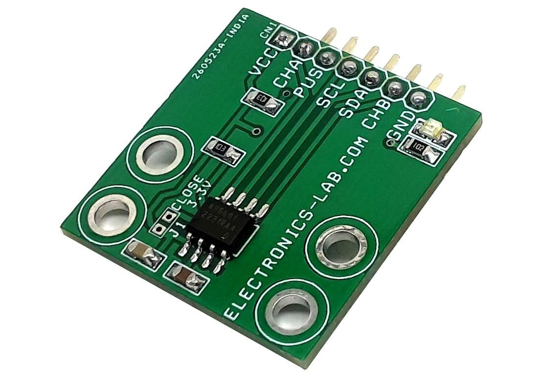
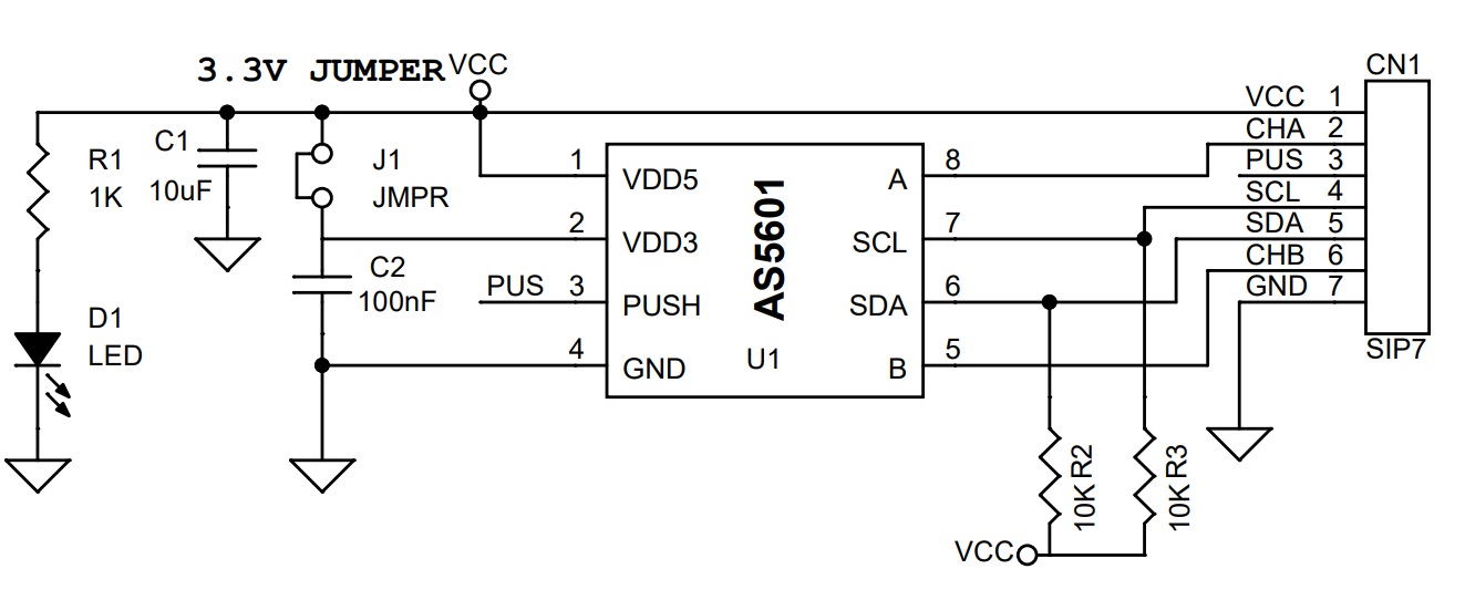
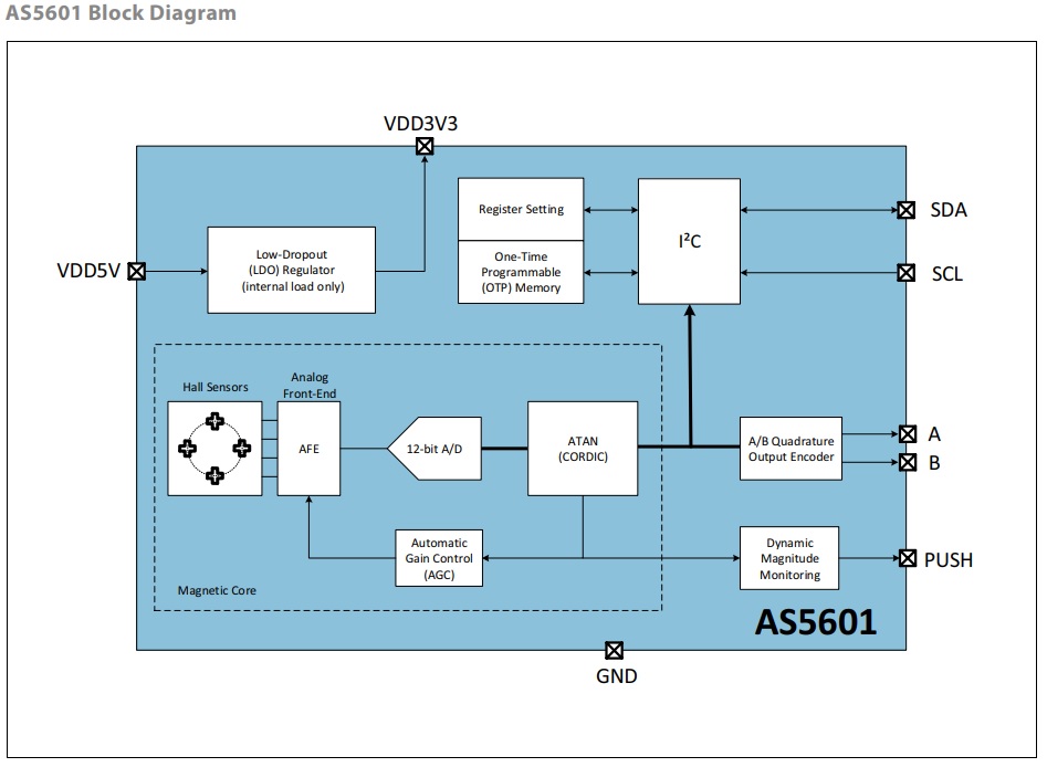
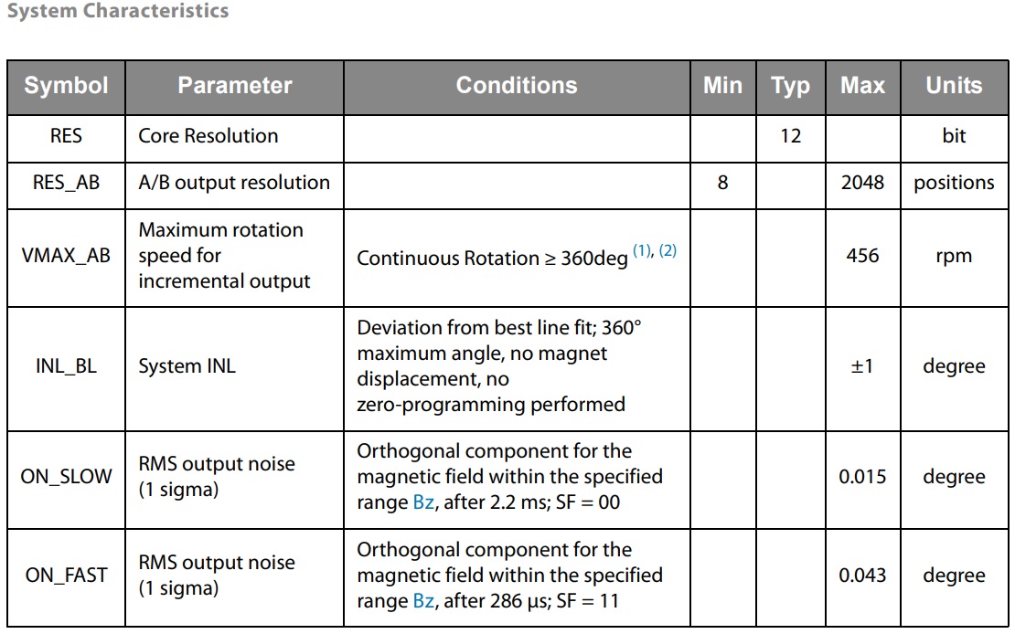
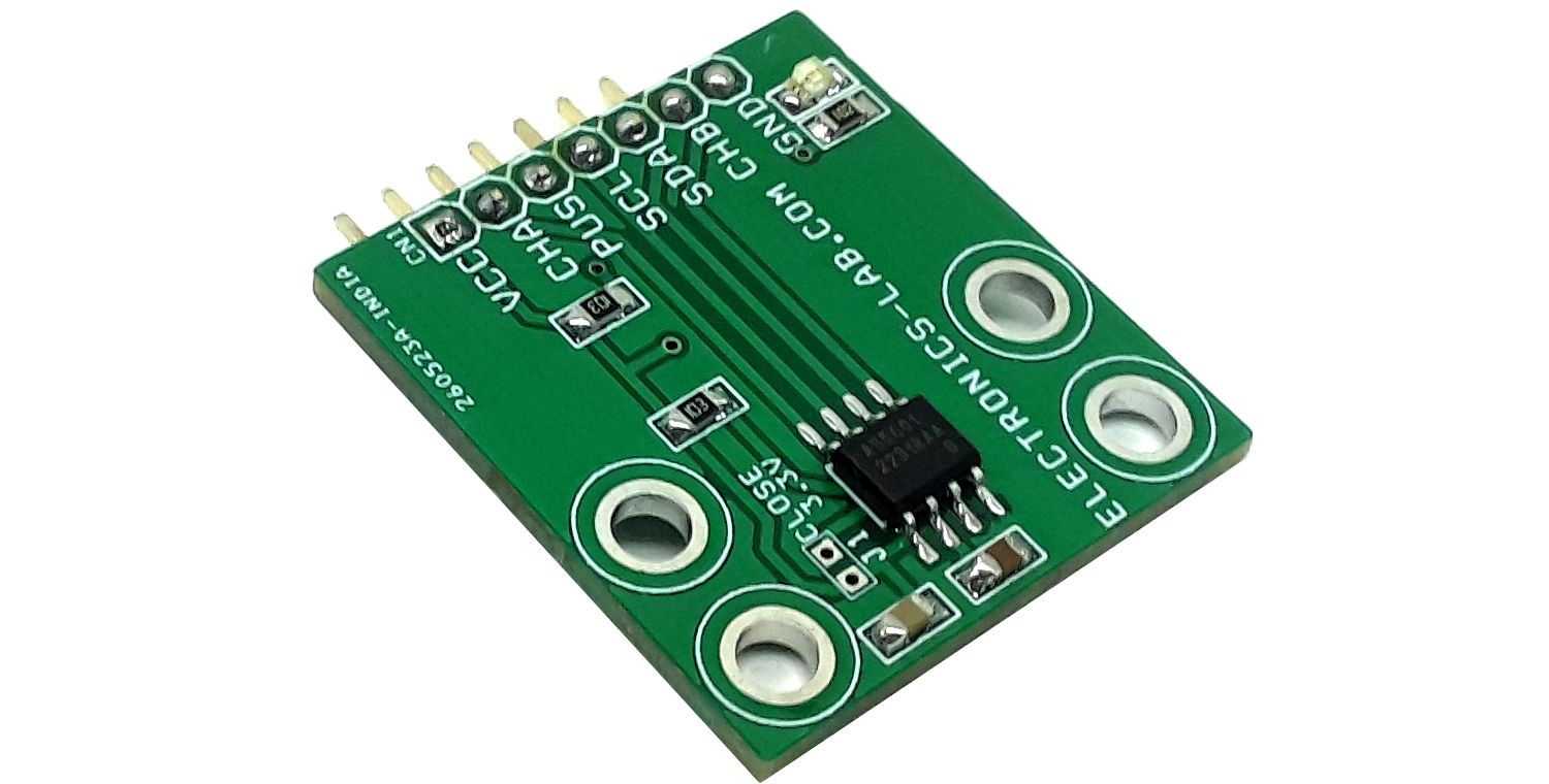
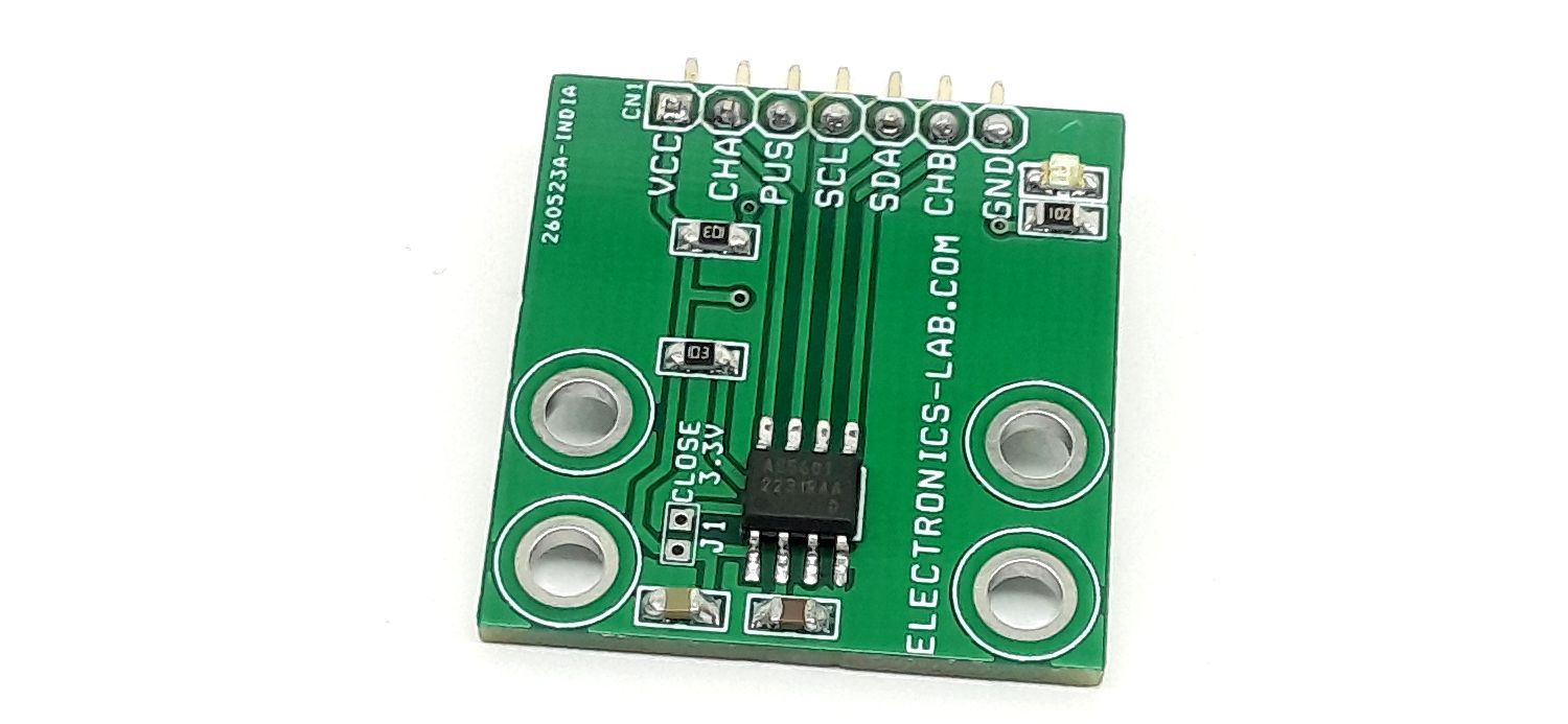
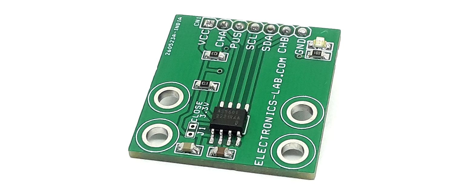
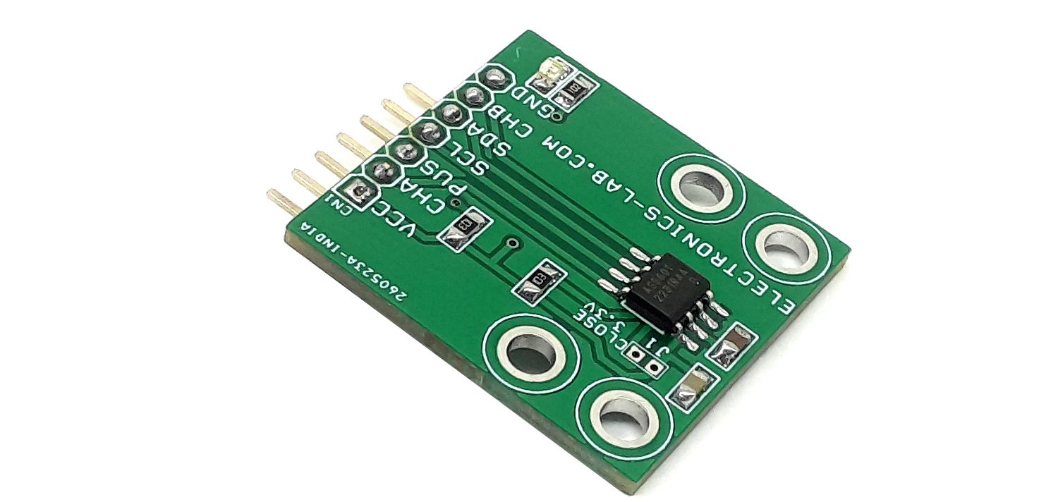
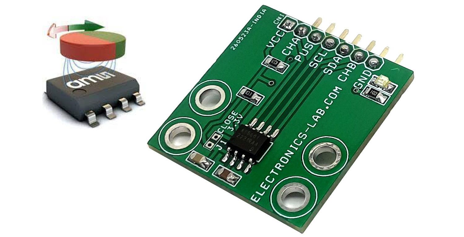
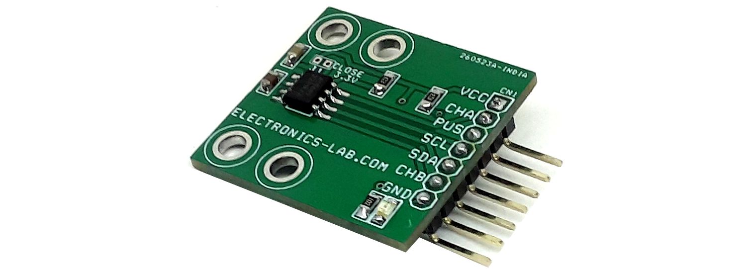
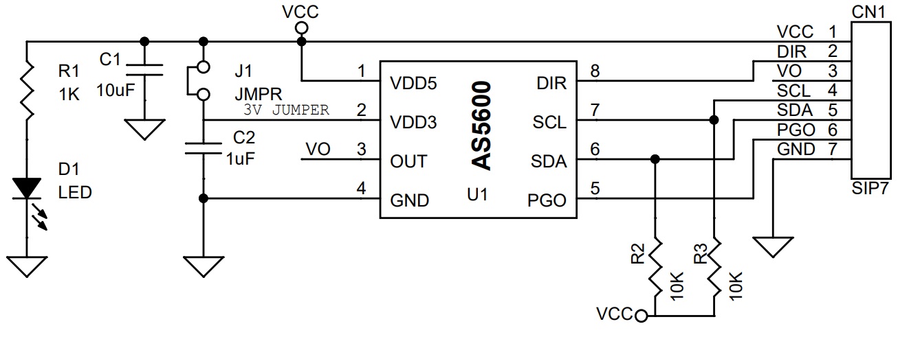
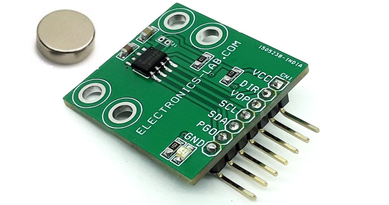
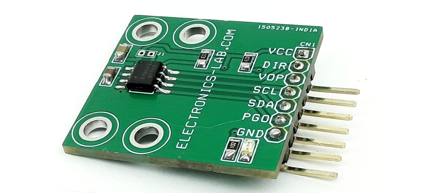
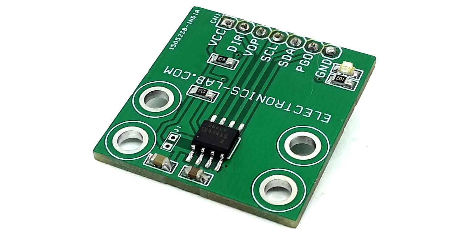
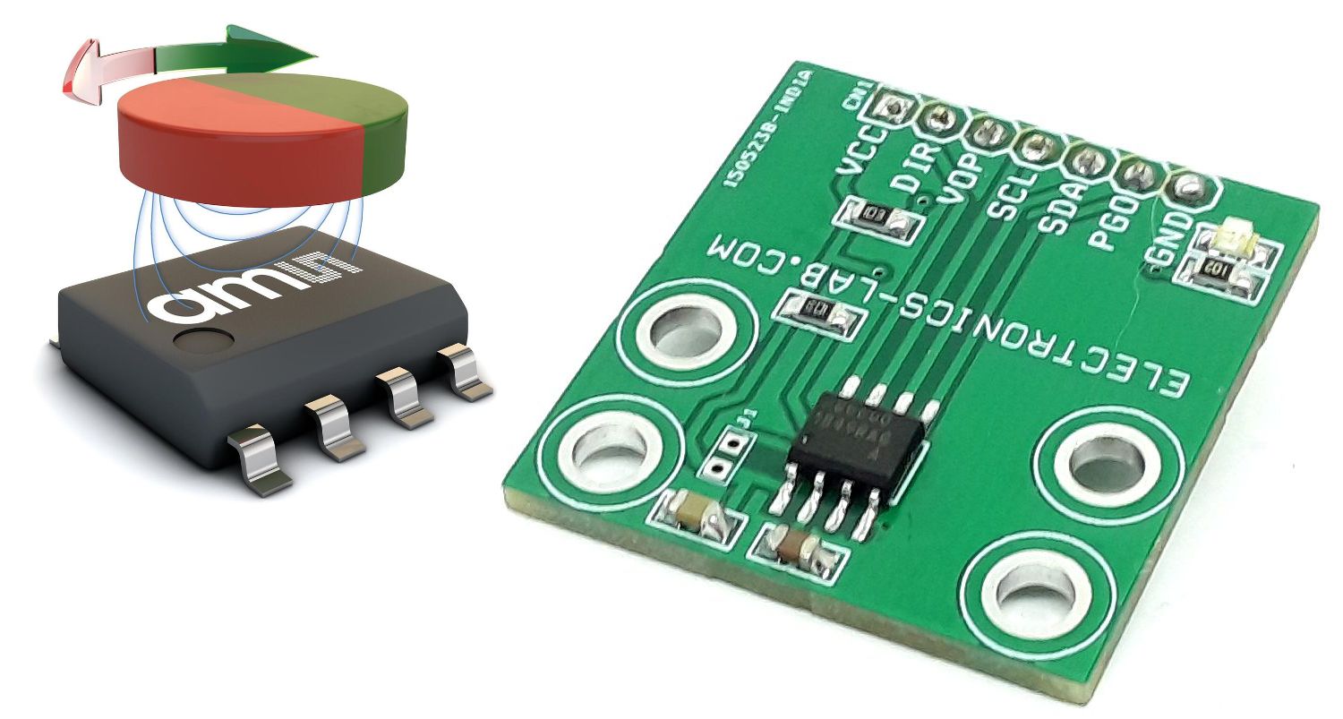
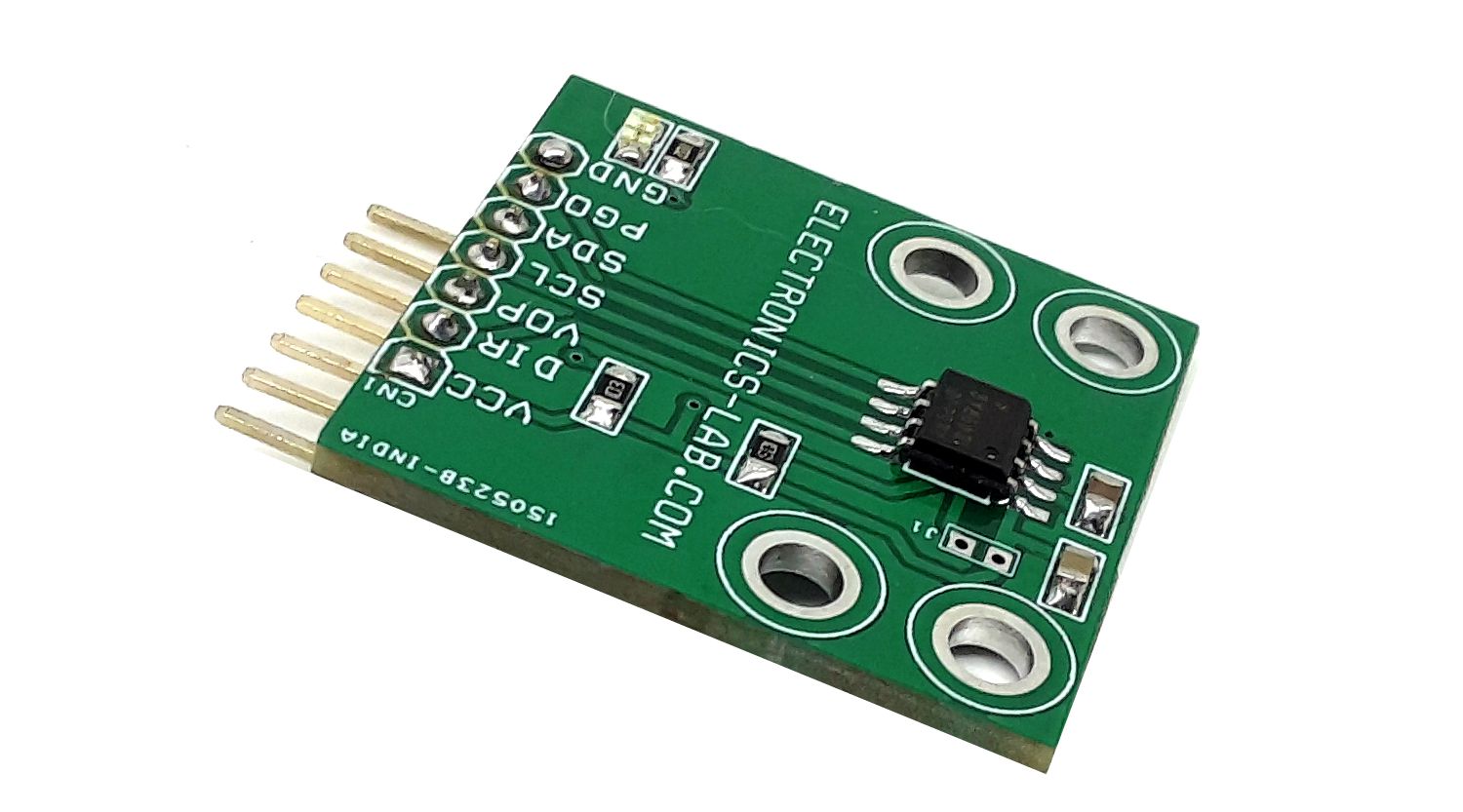
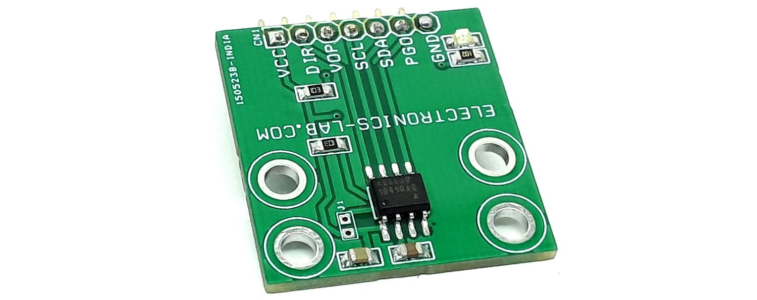
The 12-Bit programmable contactless encoder project presented here is based on AS5601 chip. This is an easy-to-program magnetic rotary position sensor module with incremental quadrature (A/B) and 12-bit digital outputs. Additionally, the PUSH output indicates fast airgap changes between the AS5601 and magnet which can be used to implement a contactless pushbutton function in which the knob can be pressed to move the magnet toward the AS5601 chip. This module is designed for contactless encoder applications, and its robust design rejects the influence of any homogenous external stray magnetic fields. Based on planar Hall sensor technology, this device measures the orthogonal component of the flux density (Bz) from an external magnet. The industry-standard I²C interface supports user programming of non-volatile parameters in the AS5601 without requiring a dedicated programmer. The AS5601 also provides a smart low-power mode which automatically reduces power consumption.
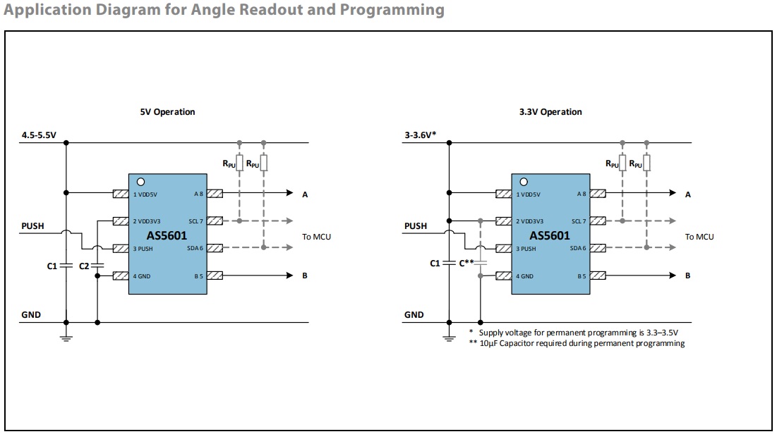
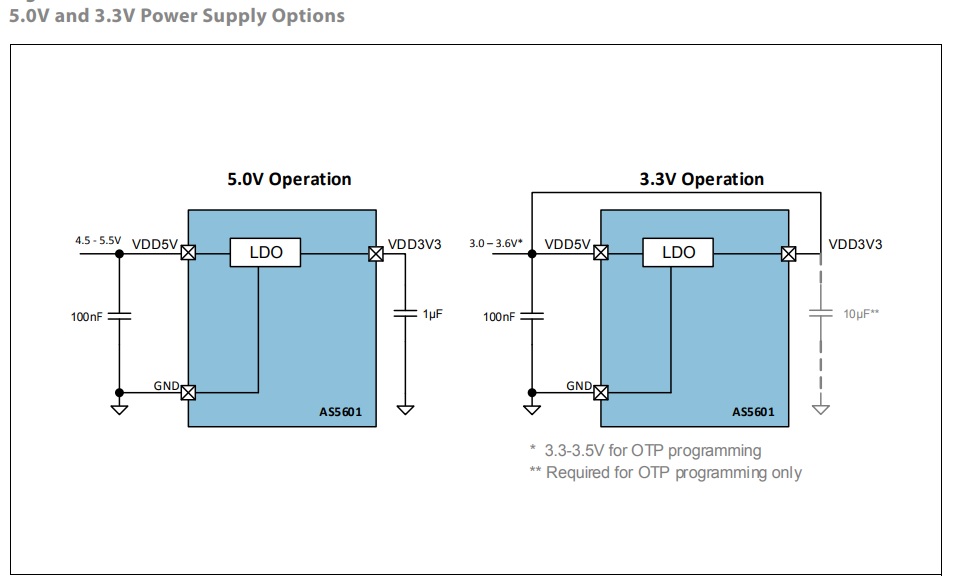
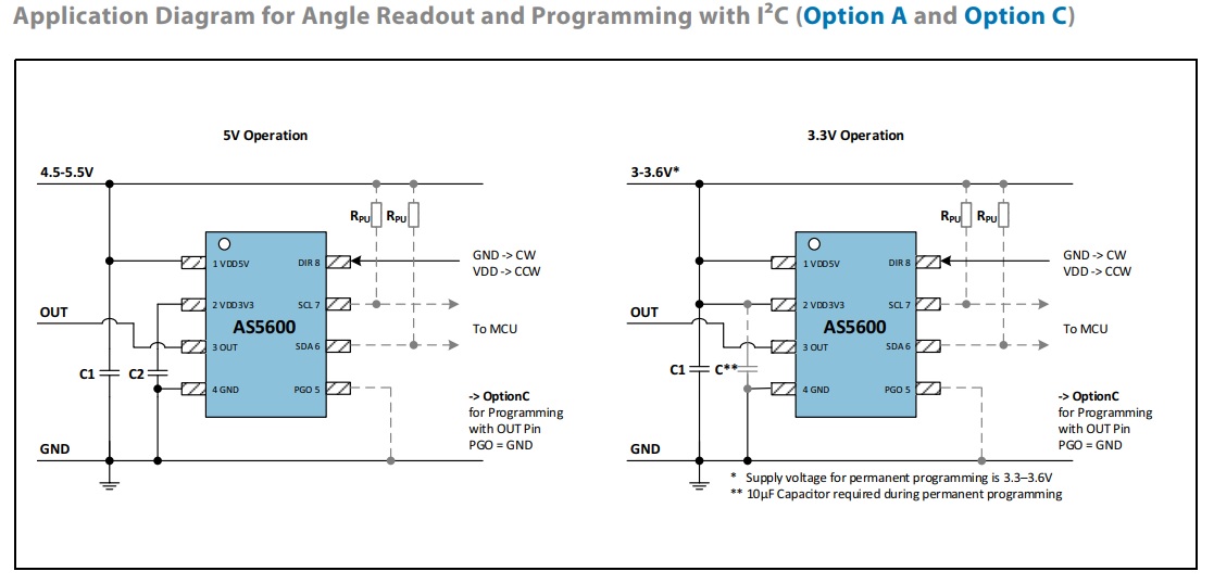
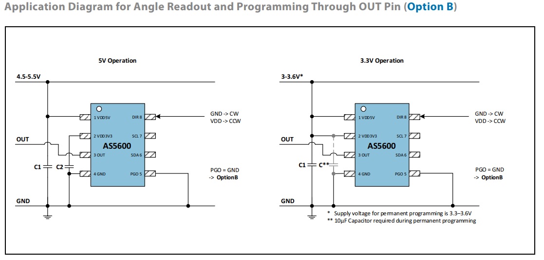
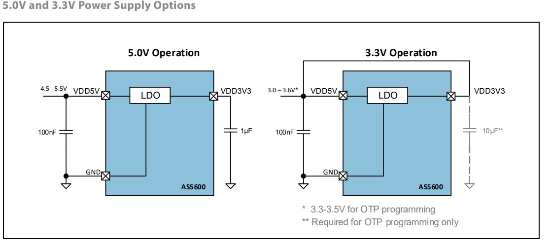
Power Management: The AS5601 is powered from a 5.0V supply using the on-chip LDO regulator, or it can be powered directly from a 3.3V supply. In 3.3V operation, the VDD5V and VDD3V3 pins must be tied together using Jumper J1. VDD is the voltage level present at the VDD5V pin.
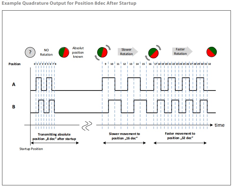
Absolute Position Feature for Quadrature Output The absolute angular position of the magnet is transmitted on the quadrature output of the position sensor after startup. By counting these pulses after startup, the absolute position within one turn of an encoder knob is known without separate initialization as shown in the Figures below.
I2C Mode: Refer to the datasheet of AS5601 chip for more information about I2C programming.
Features
Power Supply 5V or 3.3V DC
PCB Solder Jumper for 5V or 3.3V Supply Selection
Contactless angle measurement insensitive to dust and dirt
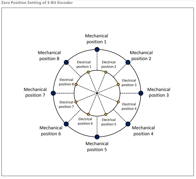
Simple user-programmable zero position and device configuration
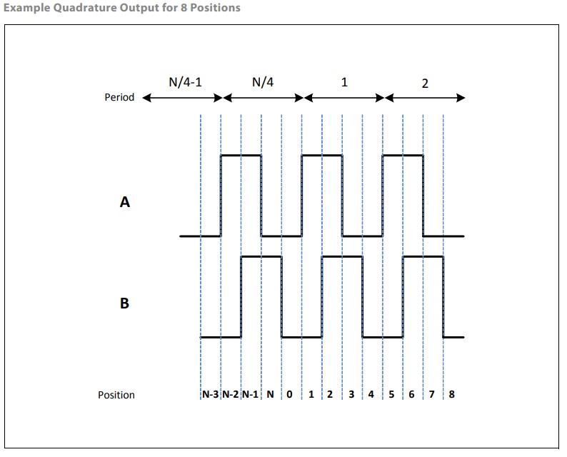
Quadrature output configurable from 8 up to 2048 positions
Pushbutton output by detecting sudden airgap changes
Automatic entry into low-power mode
Automatic magnet detection
Flexible choice of the number of A/B pulses per revolution
Simple programming
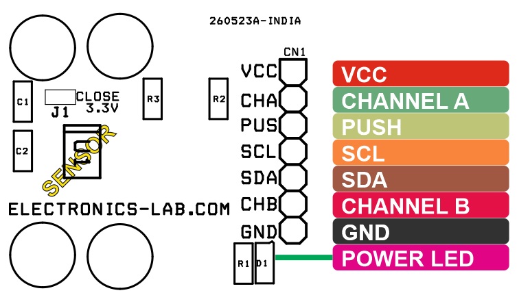
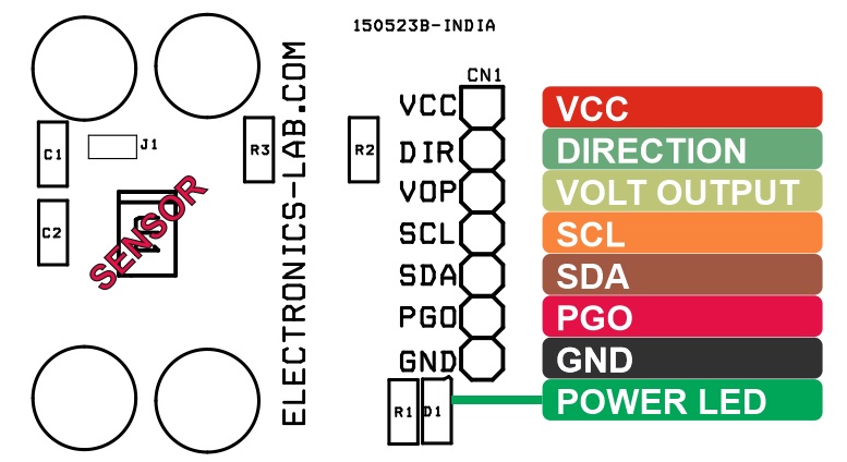
4 x 3 mm Mounting Holes
PCB Dimensions 29.21 x 27.31 mm
Applications
The AS5601 Module is ideally suited for:
Encoder replacement
Contactless rotary knobs with push buttons
Other angular position measurement solutions
Magnet Requirements
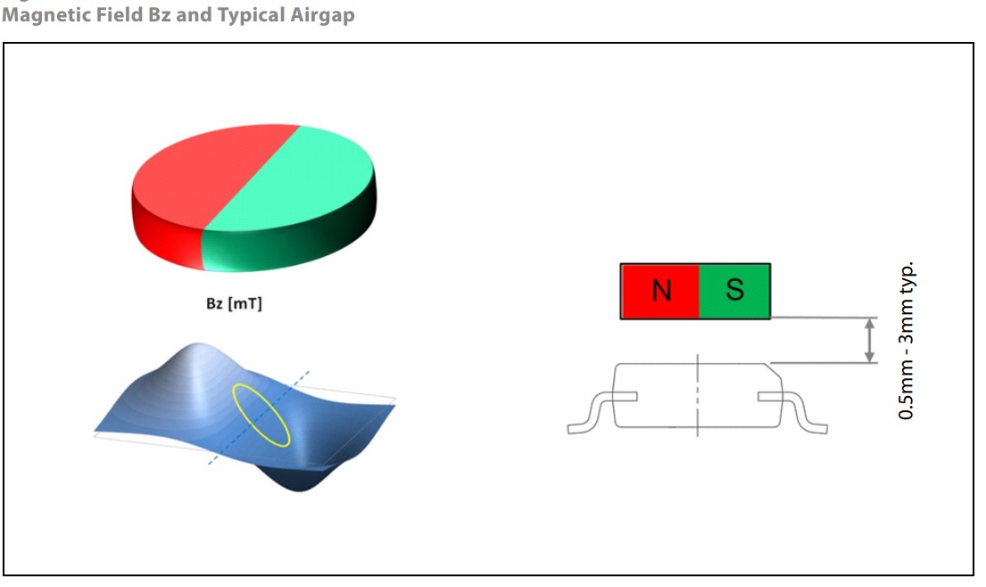
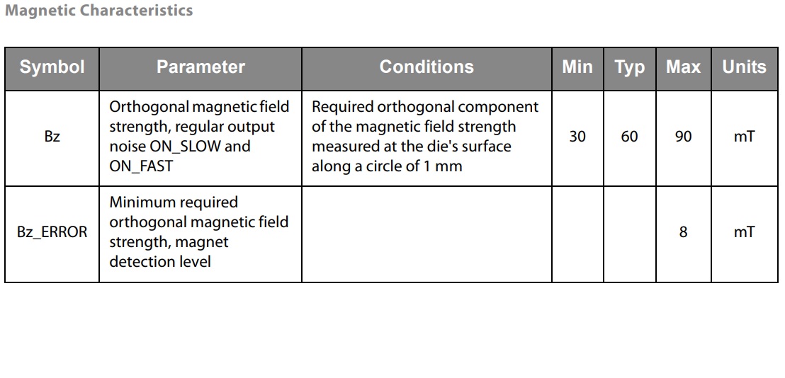
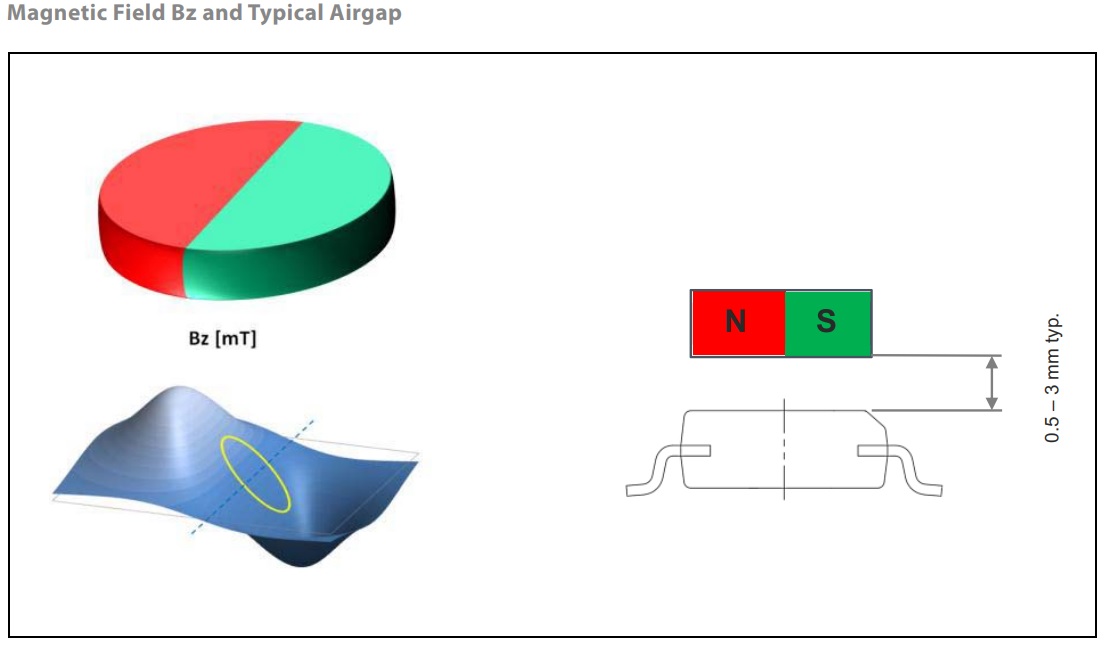
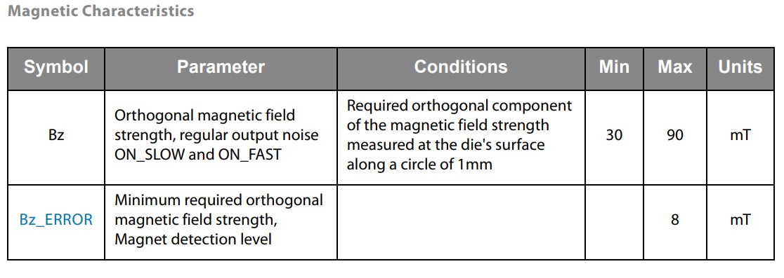
The AS5601 requires a minimum magnetic field component Bz perpendicular to the sensitive area on the chip. The center of the sensitive area is in the center of the package. Along the circumference of the Hall element circle the magnetic field Bz should be sine-shaped. The magnetic field gradient of Bz along the circle’s radius should be in the linear range of the magnet to eliminate displacement error by the differential measurement principle. The typical airgap is between 0.5 mm and 3 mm, and it depends on the selected magnet. A larger and stronger magnet allows a larger airgap. Using the AGC value as a guide, the optimal airgap can be found by adjusting the distance between the magnet and the AS5601 so that the AGC value is in the centre of its range. The maximum allowed displacement of the rotational axis of the reference magnet from the centre of the package is 0.25 mm when using a magnet with a diameter of 6mm.
Connections and Other Details
CN1: Pin 1 = VCC 5V or 3.3V, Pin 2 = Quadrature incremental signal A, Pin 3 = Push Digital Output (Contactless Push Button Function Output, Pin 4 = I2C Clock (Digital Input), Pin 5 = SDA I2C Data (Digital Input and Output), Pin 6 = Quadrature incremental signal B, Pin 7 = GND
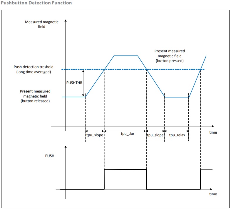
The AS5601 implements a pushbutton detection function through a dynamic and relative measurement of the orthogonal magnetic field strength. This pushbutton detection function drives the PUSH output pin high when the AS5601 detects a fast increase of the magnetic field (decrease of the airgap between the magnet and the AS5601). After a fast decrease in the magnetic field, the PUSH output is driven low.
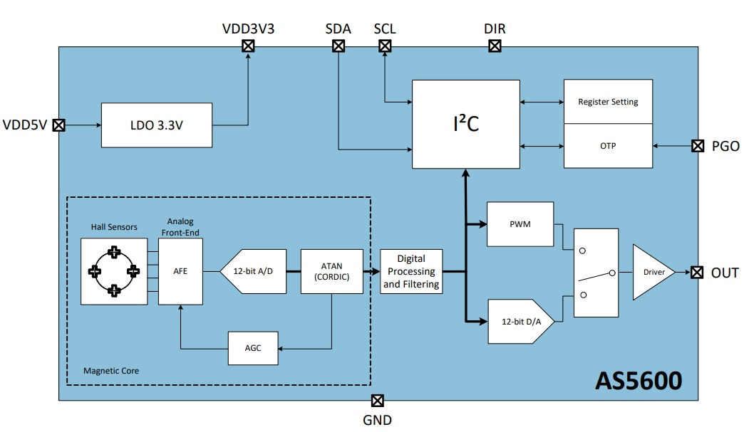
The AS5601 is a Hall-based rotary magnetic position encoder that converts the magnetic field component perpendicular to the surface of the chip into voltages which are used to produce incremental A/B outputs and absolute position indication in registers that can be read over an industry-standard I²C bus. The analog signals from the Hall sensors are first amplified and filtered before being converted by the analog-to-digital converter (ADC) into binary data. The output of the ADC is processed by the hardwired CORDIC block (Coordinate Rotation Digital Computer) to compute the angle and magnitude of the magnetic field vector. The intensity of the magnetic field is used by the automatic gain control (AGC) to adjust the amplification level to compensate for temperature and magnetic field variations. The angle value provided by the CORDIC algorithm is used by the internal logic to generate the incremental quadrature signals A and B. The magnitude and AGC value is dynamically monitored and generates the PUSH output for fast changes of the airgap between the magnet and the AS5601. Very slow changes are suppressed to provide a robust and reliable pushbutton output that tolerates temperature variation and magnet degradation. The AS5601 is programmed through an industry-standard I²C interface to write an on-chip one-time programmable (OTP) memory. This interface can be used to program a zero angle and to configure the chip.
I²C Interface
The AS5601 supports the 2-wire Fast-mode Plus I²C-slave protocol in device mode, in compliance with the NXP Semiconductors (formerly Philips Semiconductors) specification UM10204. A device that sends data onto the bus is a transmitter and a device receiving data is a receiver. The device that controls the message is called a master. The devices that are controlled by the master are called slaves. A master device generates the serial clock (SCL), controls the bus access, and generates the START and STOP conditions that control the bus. The AS5601 always operates as a slave on the I²C bus. Connections to the bus are made through the open-drain I/O lines SDA and the input SCL. Clock stretching is not included. The host MCU (master) initiates data transfers. The 7-bit slave address of the AS5601 is 0x36 (0110110 in binary).
Supported Modes
Random/Sequential read
Byte/Page write
Automatic increment (ANGLE register)
Standard-mode
Fast-mode
Fast–mode Plus
The SDA signal is the bidirectional data line. The SCL signal is the clock generated by the I²C bus master to synchronize sampling data from SDA. The maximum SCL frequency is 1 MHz Data is sampled on the rising edge of SCL.
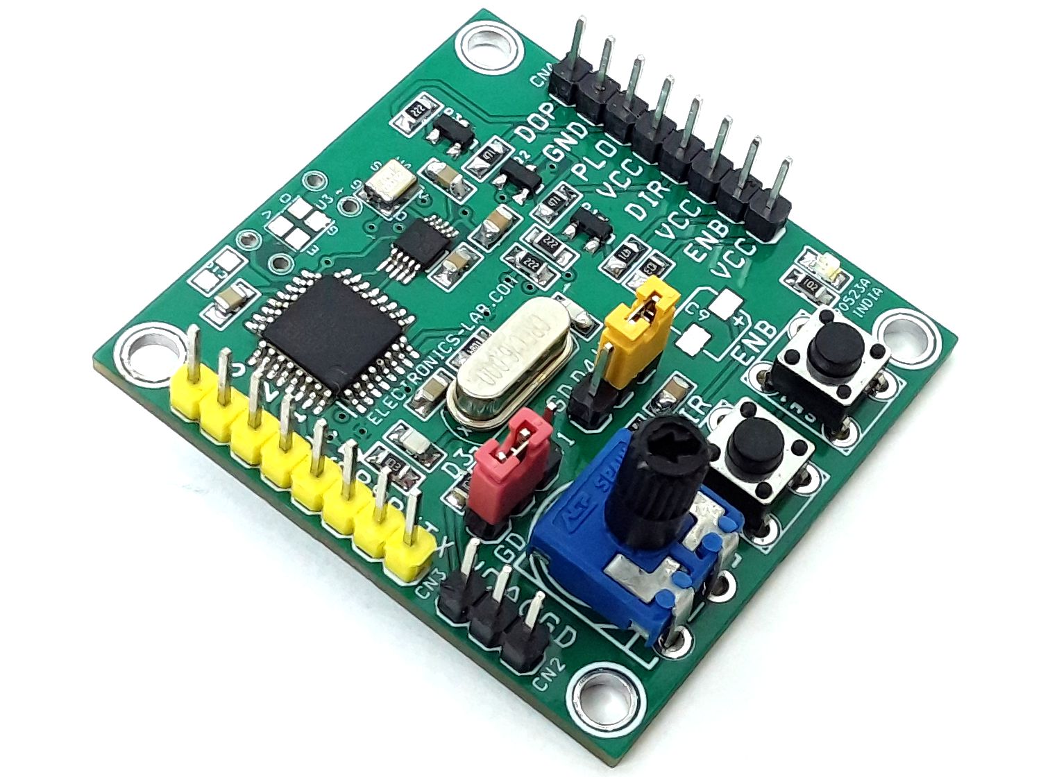
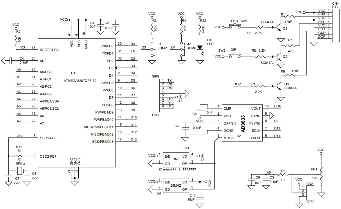
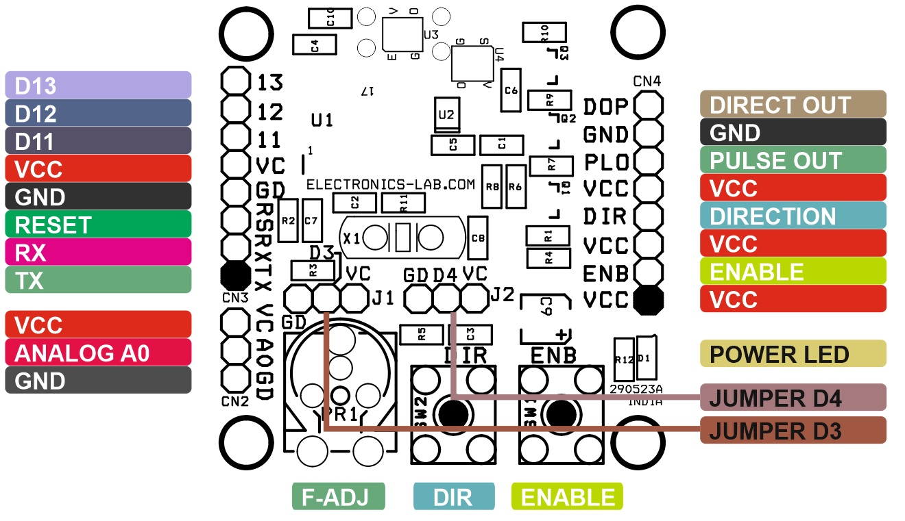
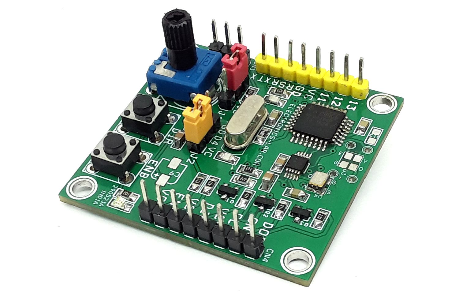
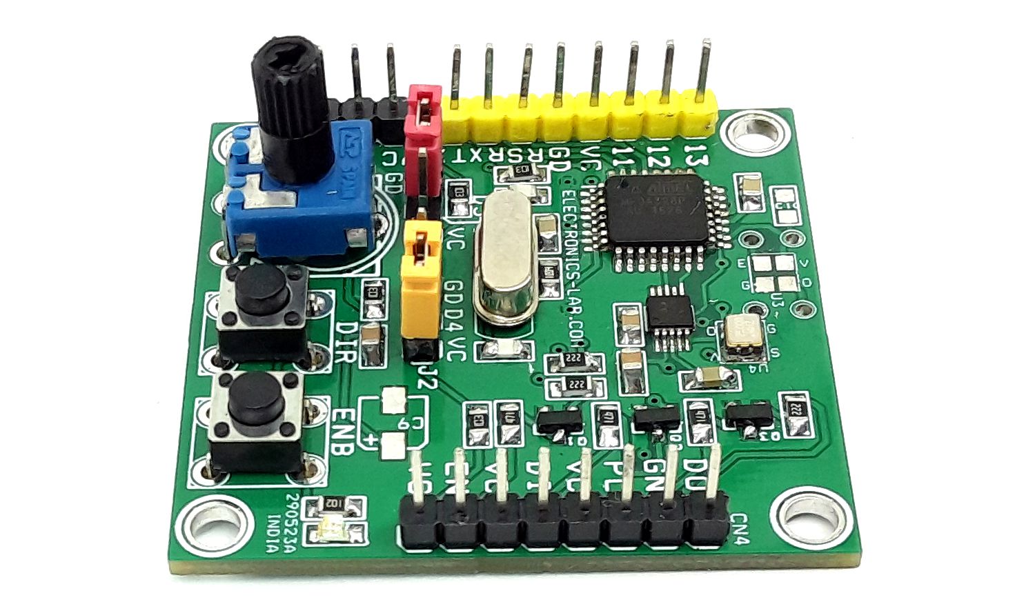
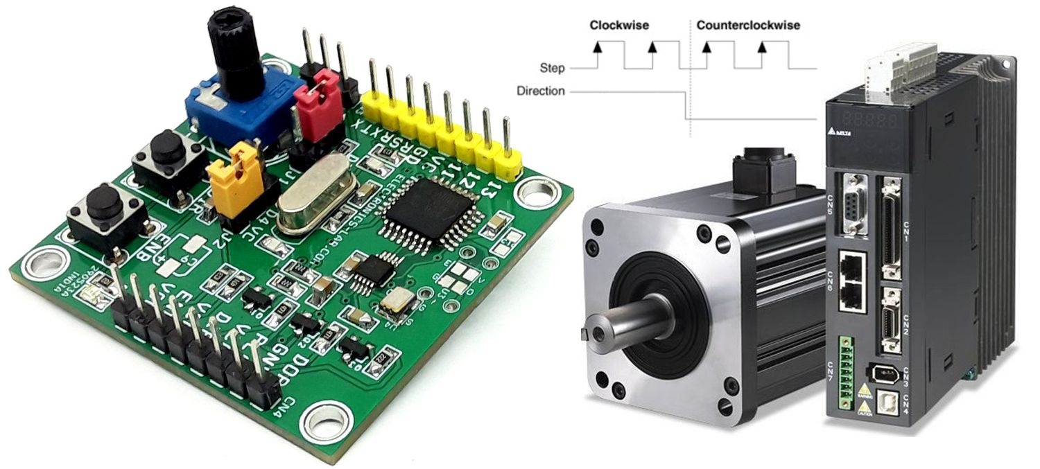
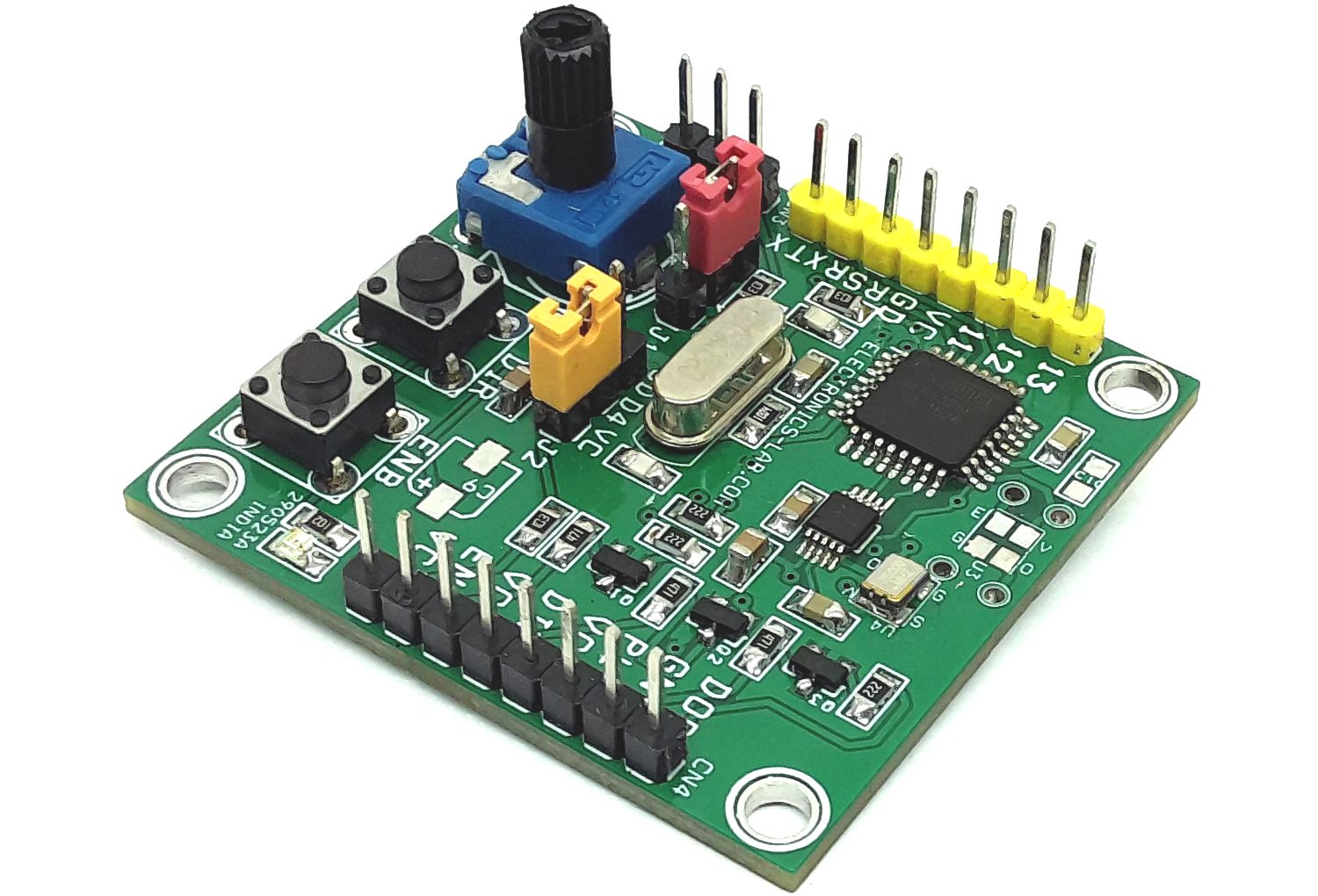
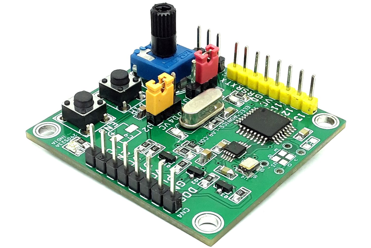
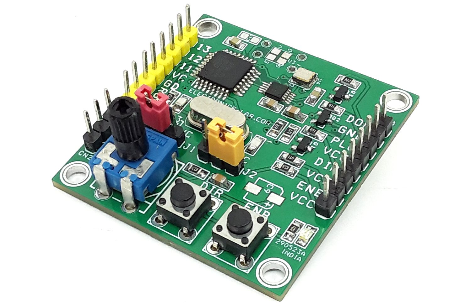
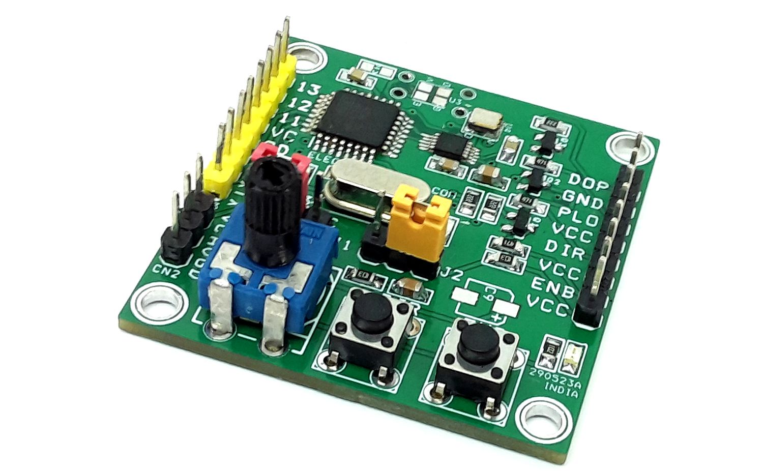
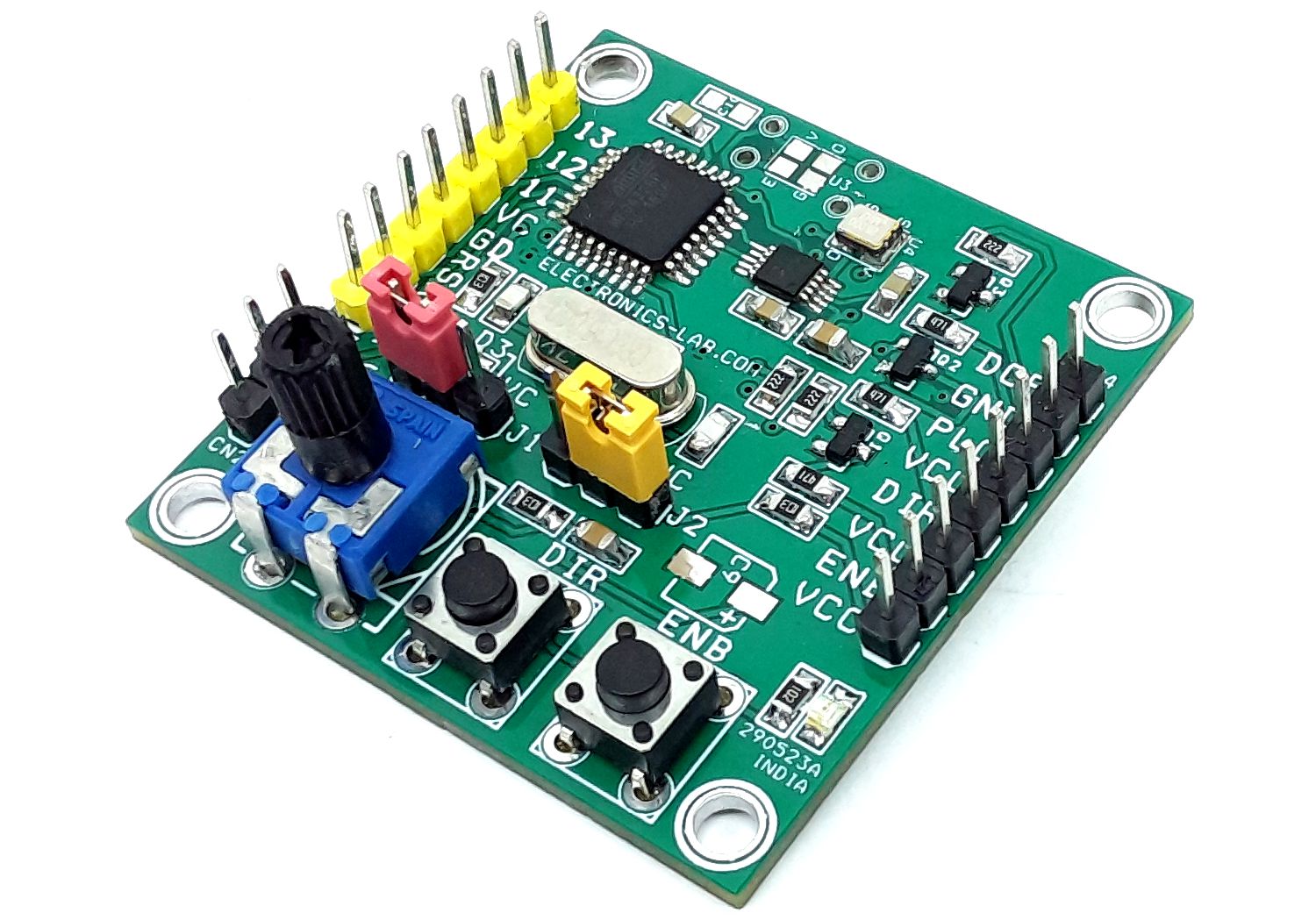
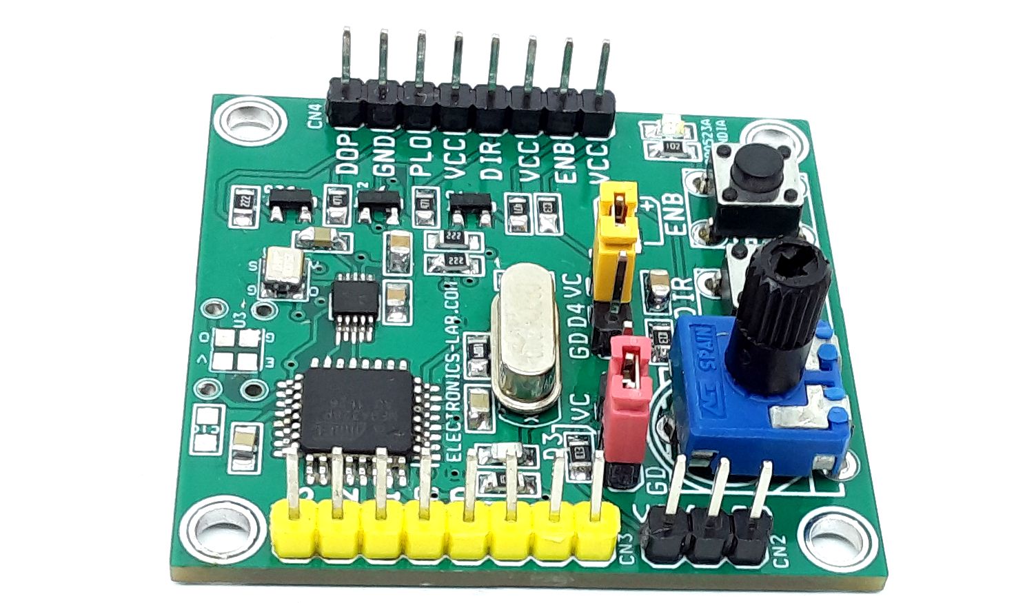
A programmable pulse generator is a very useful tool for stepper, BLDC, and AC servo drivers. Various stepper and servo drivers work with step and direction inputs. This project is the right solution to drive such drivers since it can provide a high-frequency output which is important for most AC servo drivers. The project provides a jitter-free high-frequency pulse, direction, and enable signal. The output frequency can be configured up to 12 MHz since the project is Arduino-compatible. All outputs are open collector types (5V). 2 x tactile switches are provided to set the direction and enable. An onboard trimmer potentiometer is provided to adjust the step frequency.
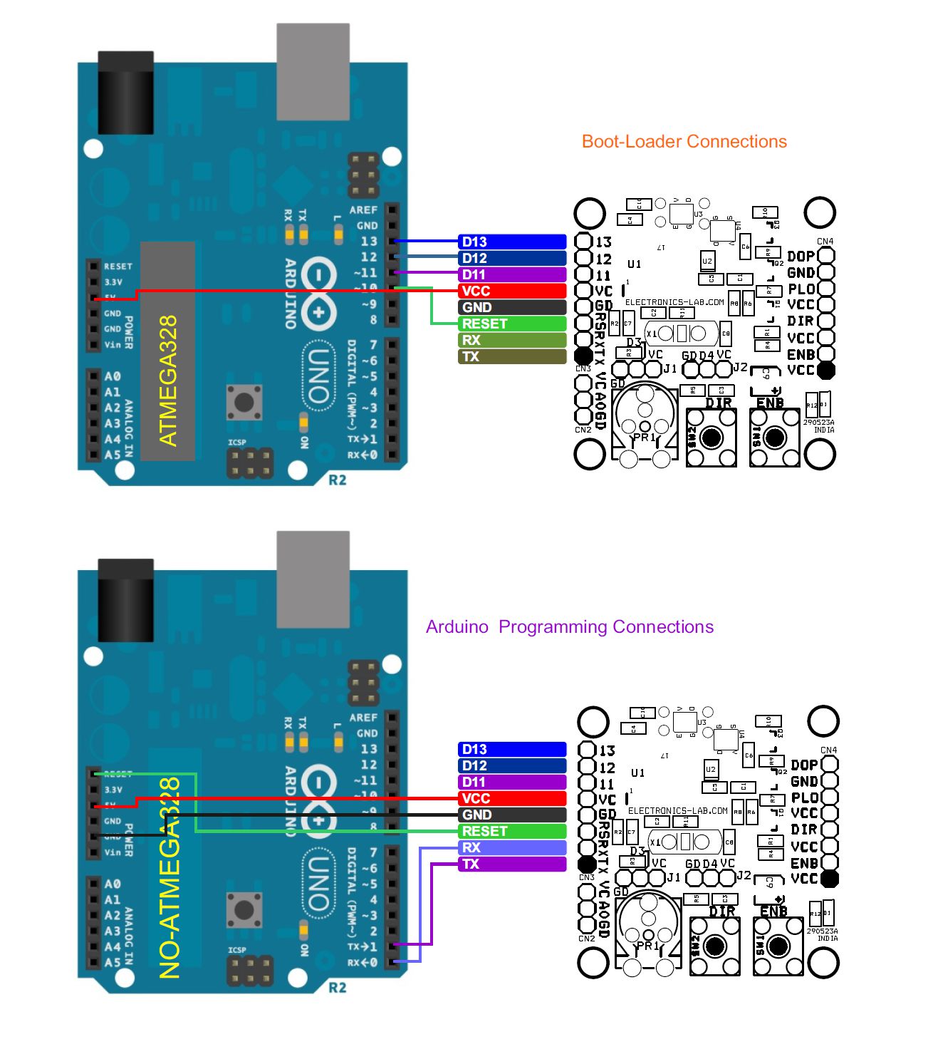
The project is Arduino compatible and consists, of an ATMEGA328 micro-controller, AD9833 DDS chip, tactile switches, and onboard trimmer pot. On-board connector provided for boot-loader and Arduino programming connector. 2 x Jumpers are connected to D3 and D4 pins of ATMEGA328. DDS chip can output high frequency up to 12Mhz.
Arduino Code
The Arduino code is available as a download below. Burn the bootloader and upload the code. The default output is 200Khz with this example code. The output frequency can be changed in Arduino code.
Arduino Pins: Digital Pin D3 and D4 Jumper J1 and J2, D9 = AD9833 FYNC, D11 = AD9833 SDATA, D13 = AD9833 SCLK
Features
Supply 5V DC
Current Consumption 30mA
Output Frequency 200Khz (Range Up to 12Mhz) – Open Collector
Pulse, Enable, Direction Outputs are Open Connector TTL Type
Direct Output from AD9833 Square wave TTL, (Triangular Wave, Sine wave = 0.6V)
On Board Enable Switch
On Board Direction Switch
On Board Power LED
On Board Trimmer Potentiometer to Adjust the Frequency
Jumpers to select the Triangular Wave, Sine Wave, Square Wave, Half Square Wave
Optional Components for Hardware Acceleration/Deacceleration (Resistor R5, and Capacitor C9)
PCB Dimensions 43.34 x 41.43 mm
4 x 3MM Mounting Holes
Frequency Generator
The board also can be used as a frequency generator. Jumpers J1 and J2 are provided to select the pulse type output. Use pin 8 of CN4 for direct output. Square output is TTL 5V, but tringle and sinewave output is lower.
Pulse Frequency
The default frequency output is 200Khz, this can be increased or decreased in Arduino code as per requirements. AD9833 supports frequencies up to 12Mhz. The output frequency is depended on the stepper driver micro-stepping setup and drive requirement; it is important to configure the required frequency in Arduino code.
Ramp
Example code doesn’t have the option to adjust the Acceleration and Deceleration. Users may include this in Arduino code. Little acceleration can be achieved with hardware changes. Install R5 10K to 100K, Install Capacitor C9 electrolytic value between 10uF to 33uF to include hardware acceleration.
Outputs
Step Pulse, Direction, and enable outputs are open collector type and TTL compatible, Direct Output of AD9833 (CN4 pin 8) is TTL for square wave and 0.6V Sinewave and Triangular Wave.
Connections and Other Details
CN1: Not Configured
CN2: External Analog Input/External Potentiometer (In this case don’t install PR1)
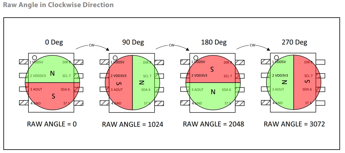
This is an easy-to-program magnetic rotary position sensor with high-resolution12-bit analog or PWM output. This contactless system measures the absolute angle of a diametric magnetized on-axis magnet. The project is designed for contactless potentiometer applications and its robust design eliminates the influence of any homogenous external stray magnetic fields. The industry-standard I²C interface supports simple user programming of non-volatile parameters without requiring a dedicated programmer. By default, the output represents a range from 0 to 360 degrees. It is also possible to define a smaller range to the output by programming a zero angle (start position) and a maximum angle (stop position). The AS5600 is also equipped with a smart low-power mode feature to automatically reduce power consumption. An input pin (DIR) selects the polarity of the output with regard to rotation direction. If DIR is connected to the ground, the output value increases with clockwise rotation. If DIR is connected to VDD, the output value increases with counterclockwise rotation.
Applications
The AS5600 Module is ideally suited for contactless potentiometers, contactless knobs, pedals, RC servos, and other angular position measurement solutions.
Standalone Operation: The module provides approx. 0 to 5V output with 0 to 360 degrees Magnet movement in standalone mode. Please refer to the datasheet of the ASM5600 chip for PWM output and programming.
Power Management: The module may be powered from a 5.0V supply using the on-chip LDO regulator, or it can be powered directly from a 3.3V supply. In 3.3V operation, the VDD5V and VDD3V3 pins must be tied together with onboard PCB solder jumper J1. VDD is the voltage level present at the VDD5V pin.
Direction (clockwise vs. counterclockwise): The AS5600 allows controlling the direction of the magnet rotation with the DIR pin. If DIR is connected to GND (DIR = 0) a clockwise rotation viewed from the top will generate an increment of the calculated angle. If the DIR pin is connected to VDD (DIR = 1) an increment of the calculated angle will happen with counterclockwise rotation.
Features
Supply 5V DC or 3.3V DC
Output 12Bit Analog or PWM Output
Default Output 0 to 5V with 0 to 360 degrees Magnet movement
Sensing Range 0 to 360 degrees
Simple user-programmable start and stop positions over the I²C interface
Maximum angle programmable from 18° up to 360°
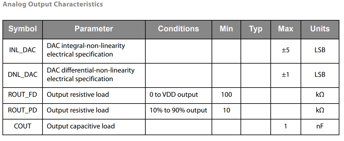
12-bit DAC output resolution
Analog output ratiometric to VDD or PWM-encoded digital output
I2C Interface for Easy Programming
Output Polarity Selection Using Dir Pin, By pulling down or Pulling Up
Automatic magnet detection
4 x 3.3MM Mounting Holes
PCB Dimensions 29.21 x 27.31 mm
Analog Output Mode
By default, the AS5600 output stage is configured as an analog ratiometric output. The Digital to Analog Converter (DAC) has 12-bit resolution. In default mode, the lower reference voltage for the DAC is GND, while the upper reference voltage is VDD. The output voltage on the OUT pin is ratiometric between GND and VDD. The maximum angular range can be programmed from 18 degrees to 360 degrees. The default range is 360 degrees. As shown below, if the range is 360 degrees, to avoid discontinuity points exactly at the limit of the range, a 10-LSB hysteresis is applied. This hysteresis suppresses toggling the OUT pin when the magnet is close to zero or 360 degrees.
PWM Output Mode
The AS5600 output stage can be programmed in the OUTS bits of the CONF register for a PWM-encoded digital output (OUTS = 10). In this mode, the OUT pin provides a digital PWM signal. The duty cycle of each pulse is proportional to the absolute angle of the rotating magnet. The PWM signal consists of a frame of 4351 PWM clock periods as shown in Figure 30. This PWM frame is composed of the following sections: • 128 PWM clock periods high • 4095 PWM clock periods data • 128 PWM clock periods low The angle is represented in the data part of the frame, and one PWM clock period represents one 4096th of the full angular range. The PWM frequency is programmed with the PWMF bits in the CONF register.
I²C Interface
The AS5600 Module supports the 2-wire Fast-mode Plus I²C-slave protocol in device mode, in compliance with the NXP Semiconductors (formerly Philips Semiconductors) specification UM10204. A device that sends data onto the bus is a transmitter and a device receiving data is a receiver. The device that controls the message is called a master. The devices that are controlled by the master are called slaves. A master device generates the serial clock (SCL), controls the bus access, and generates the START and STOP conditions that control the bus. The AS5600 always operates as a slave on the I²C bus. Connections to the bus are made through the open-drain I/O lines SDA and the input SCL. Clock stretching is not included. The host MCU (master) initiates data transfers. The 7-bit slave address of the AS5600 is 0x36 (0110110 in binary). Supported Modes • Random/Sequential read • Byte/Page write • Automatic increment (ANGLE register) • Standard-mode • Fast-mode • Fast–mode plus The SDA signal is the bidirectional data line. The SCL signal is the clock generated by the I²C bus master to synchronize sampling data from SDA. The maximum SCL frequency is 1 MHz. Data is sampled on the rising edge of SCL.
I²C Modes
Invalid Addresses There are two addresses used to access an AS5600 register. The first is the slave address used to select the AS5600. All I²C bus transactions include a slave address. The slave address of the AS5600 is 0x36 (0110110 in binary) The second address is a word address sent in the first byte transferred in a write transaction. The word address selects a register on the AS5600. The word address is loaded into the address pointer on the AS5600. During subsequent read transactions and subsequent bytes in the write transaction, the address pointer provides the address of the selected register. The address pointer is incremented after each byte is transferred, except for certain read transactions to special registers. If the user sets the address pointer to an invalid word address, the address byte is not acknowledged (the A bit is high). Nevertheless, a read or write cycle is possible. The address pointer is increased after each byte. Reading When reading from an invalid address, the AS5600 returns all zeros in the data bytes. The address pointer is incremented after each byte. Sequential reads over the whole address range are possible including address overflow. Automatic Increment of the Address Pointer for ANGLE, RAW ANGLE and MAGNITUDE Registers These are special registers which suppress the automatic increment of the address pointer on reads, so a re-read of these registers requires no I²C write command to reload the address pointer. This special treatment of the pointer is effective only if the address pointer is set to the high byte of the register. Writing A write to an invalid address is not acknowledged by the AS5600, although the address pointer is incremented. When the address pointer points to a valid address again, a successful write accessed is acknowledged. Page writes over the whole address range is possible including address overflow. Supported Bus Protocol Data transfer may be initiated only when the bus is not busy. During data transfer, the data line must remain stable whenever SCL is high. Changes in the data line while SCL is high are interpreted as START or STOP conditions.
Accordingly, the following bus conditions have been defined: Bus Not Busy Both SDA and SCL remain high. Start Data Transfer A change in the state of SDA from high to low while SCL is high defines the START condition. Stop Data Transfer A change in the state of SDA from low to high while SCL is high defines the STOP condition. Data Valid The state of the data line represents valid data when, after a START condition, SDA is stable for the duration of the high phase of SCL. The data on SDA must be changed during the low phase of SCL. There is one clock period per bit of data. Each I²C bus transaction is initiated with a START condition and terminated with a STOP condition. The number of data bytes transferred between START and STOP conditions is not limited, and is determined by the I²C bus master. The information is transferred byte-wise and each receiver acknowledges with a ninth bit. Acknowledge Each I²C slave device, when addressed, is obliged to generate an acknowledge after the reception of each byte. The I²C bus master device must generate an extra clock period for this acknowledge bit. A slave that acknowledges must pull down SDA during the acknowledge clock period in such a way that SDA is stable low during the high phase of the acknowledge clock period. Of course, setup and hold times must be taken into account. A master must signal an end of a read transaction by not generating an acknowledge bit on the last byte that has been clocked out of the slave. In this case, the slave must leave SDA high to enable the master to generate the STOP condition.
The AS5600 is a Hall-based rotary magnetic position sensor using planar sensors that convert the magnetic field component perpendicular to the surface of the chip into a voltage. The signals coming from the Hall sensors are first amplified and filtered before being converted by the analog-to-digital converter (ADC). The output of the ADC is processed by the hardwired CORDIC block (Coordinate Rotation Digital Computer) to compute the angle and magnitude of the magnetic field vector. The intensity of the magnetic field is used by the automatic gain control (AGC) to adjust the amplification level to compensate for temperature and magnetic field variations. The angle value provided by the CORDIC algorithm is used by the output stage. The user can choose between an analog output and a PWM-encoded digital output. The former provides an output voltage that represents the angle as a ratiometric linear absolute value. The latter provides a digital output which represents the angle as the pulse width. The AS5600 is programmed through an industry-standard I²C interface to write an on-chip non-volatile memory. This interface can be used to program a zero angle (start position) and a maximum angle (stop position) which maps the full resolution of the output to a subset of the entire 0 to 360 degrees range.
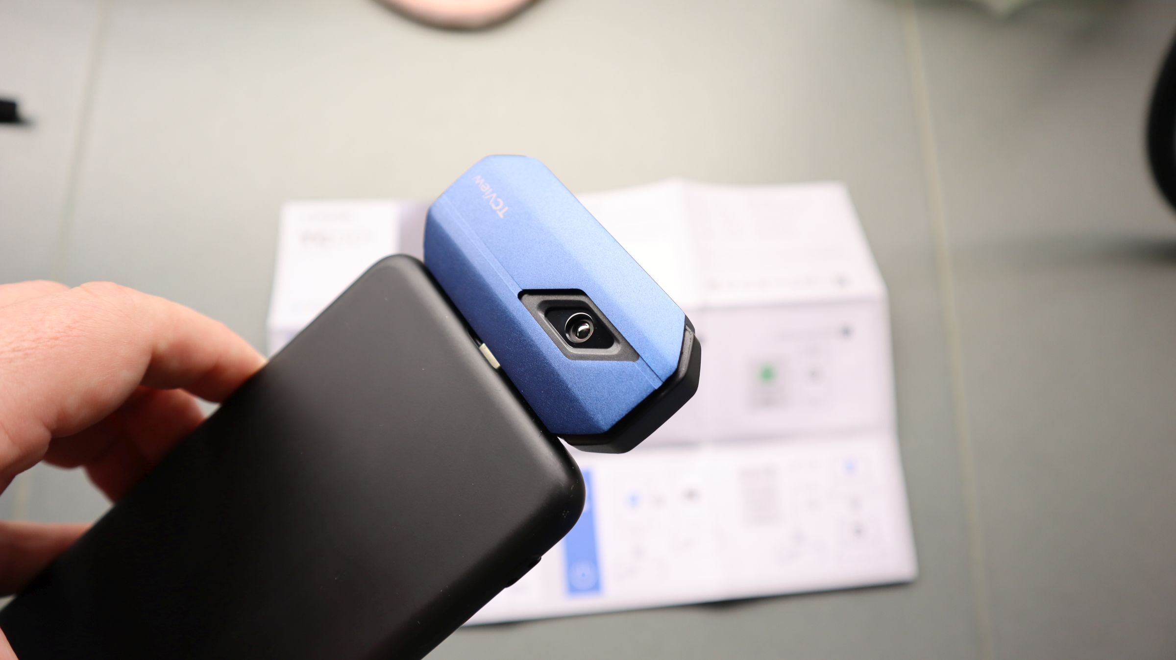
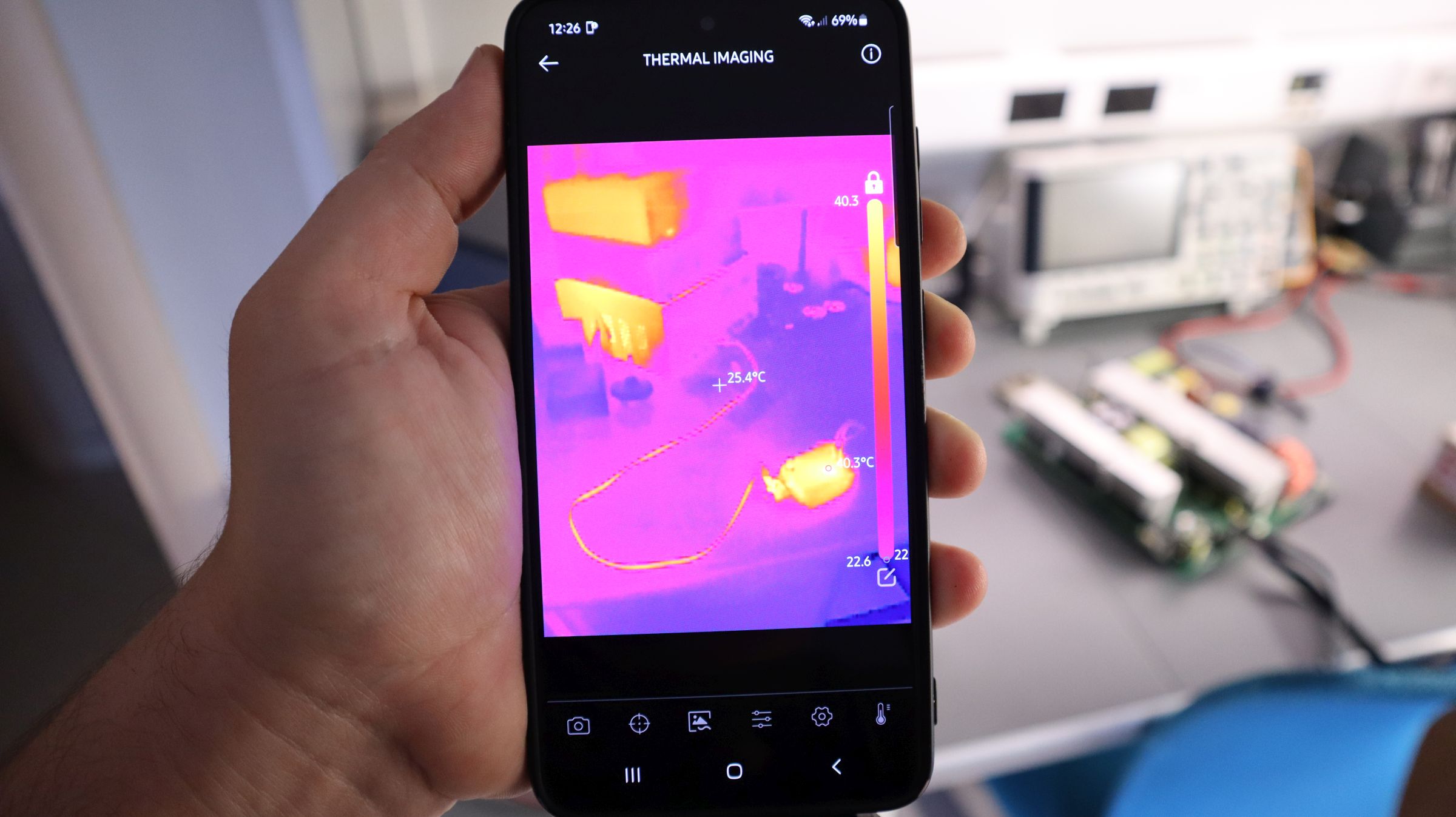
Having your very own infrared thermal camera is very desirable. Previously, it was quite challenging to come across any options priced below $500. Even among those options, many had limited vertical resolutions of 100 pixels or less and subpar screens. However, there is now an intriguing alternative available: the TOPDON TC001 Thermal Camera. It offers nearly half the cost of smartphone-attached thermal cameras.
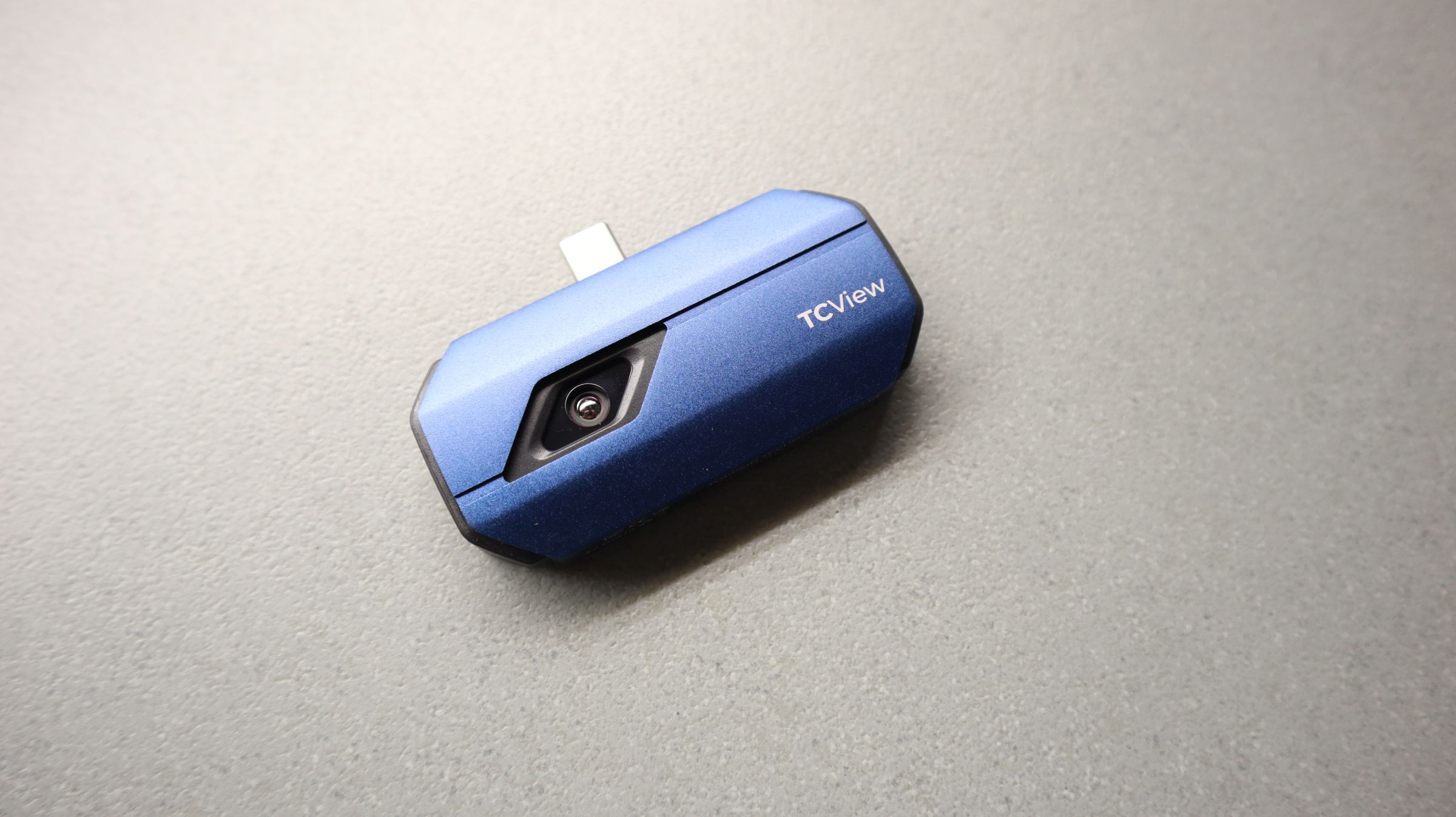
TOPDON TC001 Thermal Camera
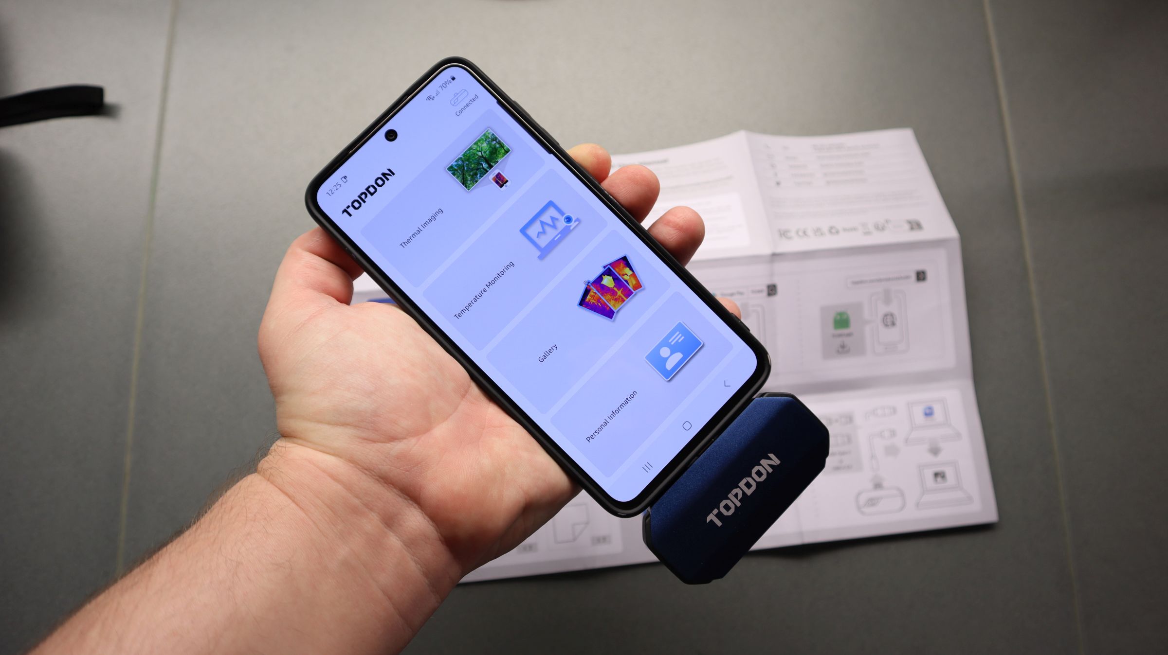
The TOPDON TC001 Thermal Camera is specifically developed as an infrared thermal camera, intended for compatibility with Android phones, Windows computers, and laptops. It conveniently connects to a phone using a USB-C connection. By utilizing the TOPDON software, users can view a thermal representation of the scene they are observing. The camera enables capturing images and videos, monitoring temperature changes over a period, and offers a variety of additional features through the accompanying app.
Features
Display a clear thermal image with an ultra-high infrared resolution of 256×192 pixels.
View detailed temperature changes with high heat sensitivity of 40mk.
Perform temperature detection with extreme accuracy, with a maximum of ±3.6℉ (2℃) temperature variance.
Read temperatures on objects ranging from -4℉ to 1022℉ (-20℃ to 550℃).
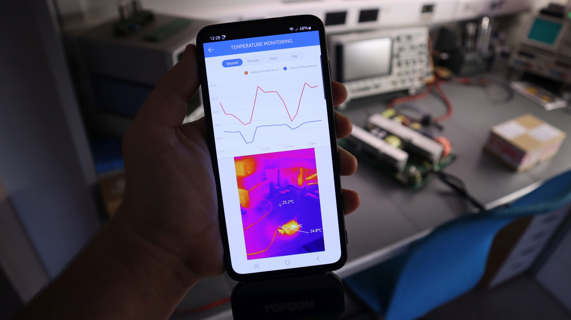
Manually select 3 dimensions to check the temperature: Point, Line (Highest and Lowest), and Surface (Highest and Lowest).
Monitor temperature change by a waveform graph.
Choose from a variety of color palettes for a more interactive experience.
Adjustable upper and lower limits, and corresponding colors to view temperatures intuitively.
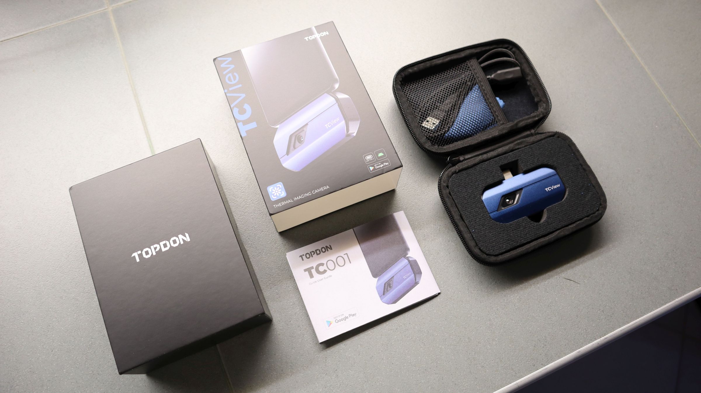
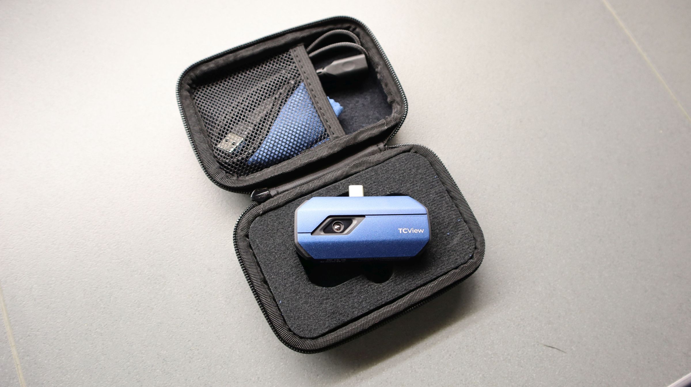
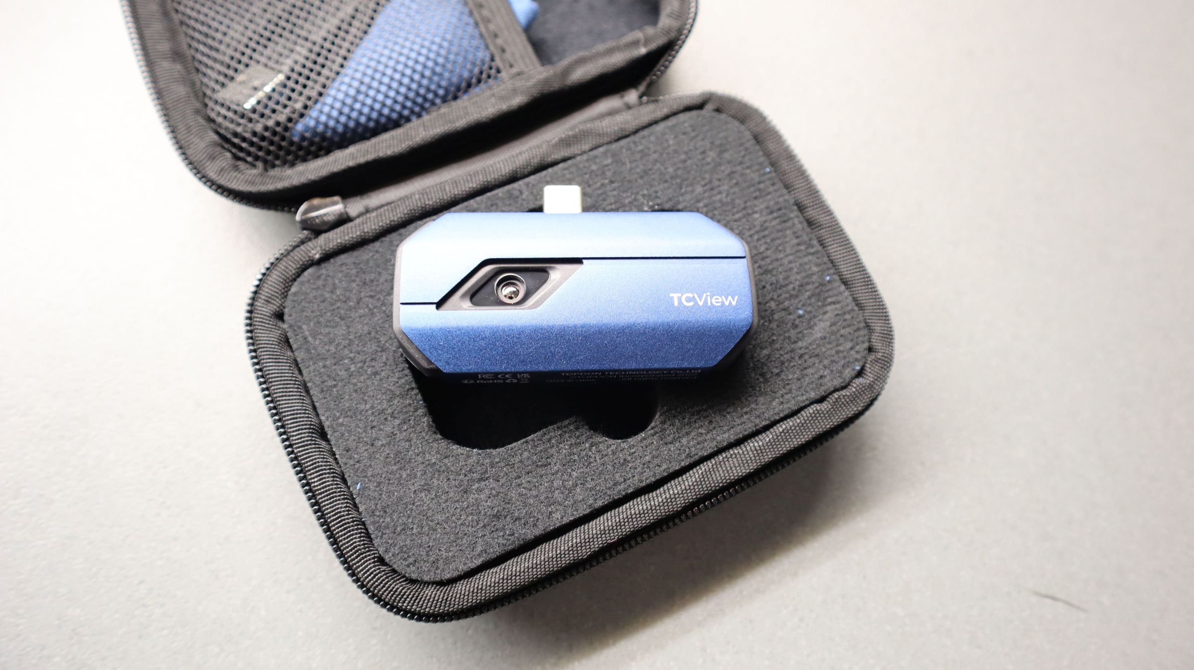
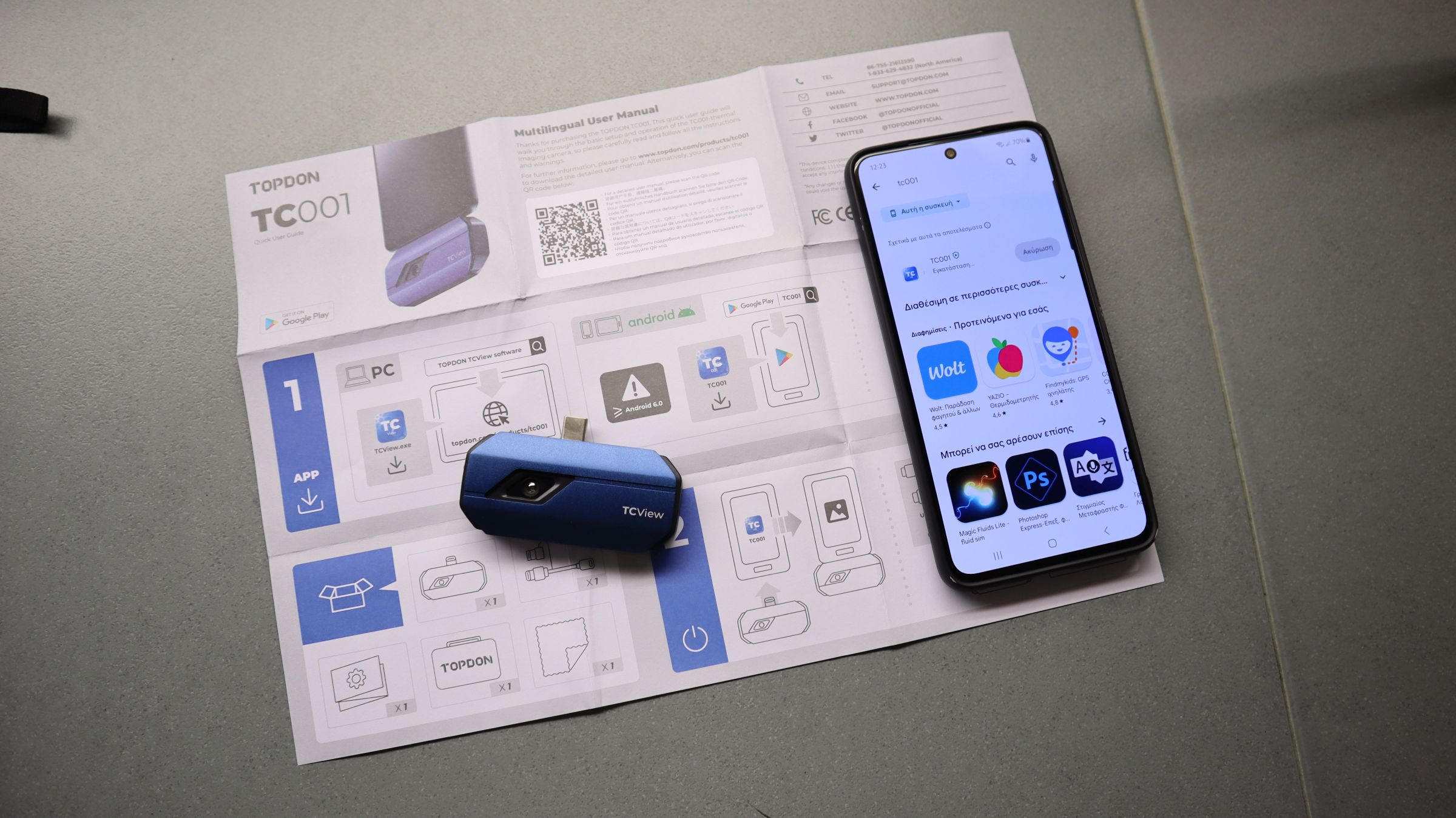
As you unpack the TOPDON TC001, you will discover the following items:
The TOPDON TC001 Thermal Camera
A USB extension cable with a USB-C to USB-A converter
A cleaning cloth
A carrying case
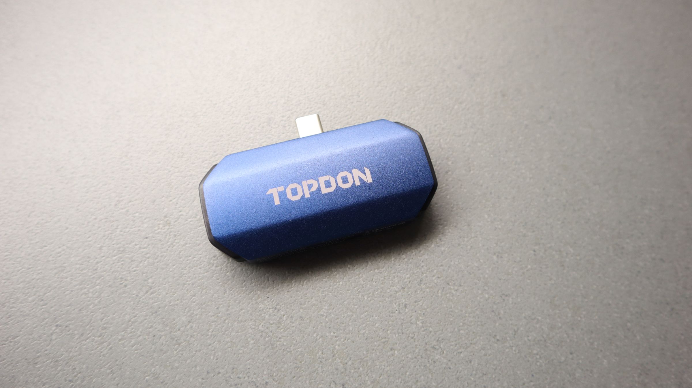
The dimensions of the TOPDON TC001 Thermal Camera are approximately 2.75″ x 1.75″ x 0.5″, making it a compact rectangular device. The thermal camera is located on the front-facing side of the unit. The top portion of the camera features a USB-C connection that is slightly longer than usual. This design ensures compatibility with phones, even if they have a moderately thick protective case. The backside of the TOPDON TC001 Thermal Camera is adorned with a simple TOPDON logo. The device is constructed with a combination of aluminum and plastic materials, providing a solid and durable feel.
Android App
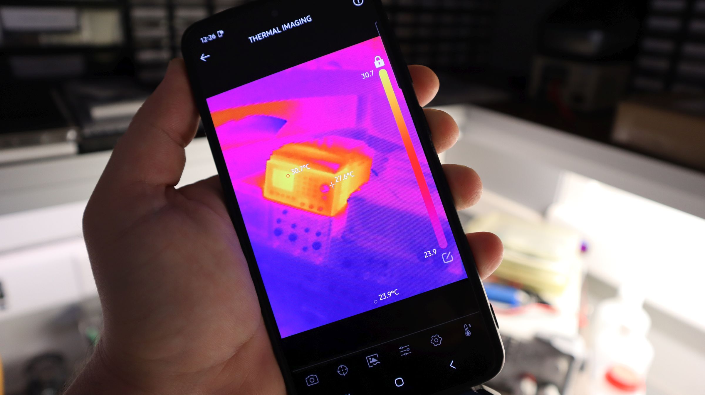
In order to utilize the TOPDON TC001 Thermal Camera, you have two options: connecting it to an Android phone that supports OTG (On-The-Go) or a Windows PC. For my testing purposes, an Android phone will be used. To begin, you will need to download and install the TC001 app from the Google Play app store, which is a straightforward process.
After completing the installation process, you will be greeted with a screen that closely resembles the interface of a standard camera application on your mobile phone. However, by default, everything will be displayed in different shades of red. Within the app, you have the option to change the color palette to your preference. Additionally, you can capture images and videos, and make adjustments to various settings. For instance, you have the flexibility to narrow down the temperature detection range, allowing you to exclude temperatures that fall outside a specific range. We tested the Android App and we have to tell you that it’s very well-designed, operates fast, and has some features we haven’t seen on other thermal camera Apps. One of these features is the track and log the temperature of an object and show the results on a graph. Other features of the app include:
DIY Temperature Range: Featuring a DIY temperature range ability, the TC001 allows users to set upper and lower limits, and corresponding color images will display when the object temperature exceeds this range. DIY Temperature Upper and Lower Limits: Only a separate upper or lower limit can be set, there is no longer a limit to 2 at the same time.
Three Temperature-Reading Dimensions: Users can manually select 3 dimensions to check the temperature in the TC001 App: Point, Line (Highest and Lowest) and Surface (Highest and Lowest) dimensions. The 3 areas for each dimension, allow users to read temperatures in 9 areas simultaneously. When connected to a tablet, more areas can be tested with the Unlimited Dimension selection.
Multiple Color Palettes: This thermal imaging tool offers 10 unique color palettes for mobile users to customize a temperature display. Users can read the temperature differences in a scene with the gradient colors of their choice. When using a tablet, 99 color palettes are available, offering more possibilities.
New Temperature Bar Switch: Now users have the ability to turn on the temperature bar when taking pictures. Once the temperature bar is toggled on, it will remain displayed so that users can easily distinguish between the highest and lowest temperature in the picture, as well as which pseudo-color is selected.
Shutter Switch Sound: According to user feedback, many do not like to hear the shutter click when using the camera. Users are now able to manually close the shutter.
Example Applications
The application of the TOPDON TC001 Thermal Camera is endless. You can use it to assess the insulation quality in your house. It will provide you with prompt insights into which windows and doors were potentially responsible for the most significant air leakage, indicated by variations in floor and ceiling temperatures compared to the rest of the house. The camera also proves helpful in swiftly identifying studs within the walls.
In general, the TOPDON TC001 Thermal Camera fulfills all the expectations one would have for it: it effectively displays and captures high-quality thermal images to serve diverse needs and purposes. Its compatibility with Android or iOS phones ensures convenient accessibility whenever I wish to examine thermal aspects.
In general, thermal cameras have various applications in the field of electronics engineering as well. Here are some examples:
Fault detection and troubleshooting: Thermal cameras can be used to detect faulty components or connections in electronic circuits. By detecting temperature variations, they can help identify overheating components or areas with poor electrical contact.
PCB analysis: Printed Circuit Boards (PCBs) are crucial components in electronic devices. Thermal cameras can be used to analyze the thermal distribution on PCBs, identifying hotspots that may indicate areas of concern such as inadequate cooling or excessive power dissipation.
Quality control: Thermal cameras can be employed in the quality control process of electronic devices. By inspecting the thermal signatures of products during manufacturing or testing, they can identify defects like improper soldering, short circuits, or damaged components.
Energy efficiency analysis: Thermal cameras can assist in evaluating the energy efficiency of electronic devices. They can measure heat dissipation, identify energy losses, and optimize designs to improve overall efficiency.
Environmental testing: Electronic devices often need to operate in diverse environments. Thermal cameras can be used to simulate and analyze extreme conditions such as temperature cycling or thermal shock tests, ensuring the devices can withstand such conditions without performance degradation or failure.
Thermal management: Efficient thermal management is critical in electronic systems to prevent overheating and ensure proper functioning. Thermal cameras can help evaluate the effectiveness of cooling mechanisms, such as heat sinks or fans, by visualizing temperature distribution and identifying areas with inadequate heat dissipation.
Electronic component testing: Thermal cameras can be used to test electronic components for proper operation and performance. By monitoring temperature variations, they can detect anomalies, faults, or potential failure points in components like transistors, ICs, or power devices.
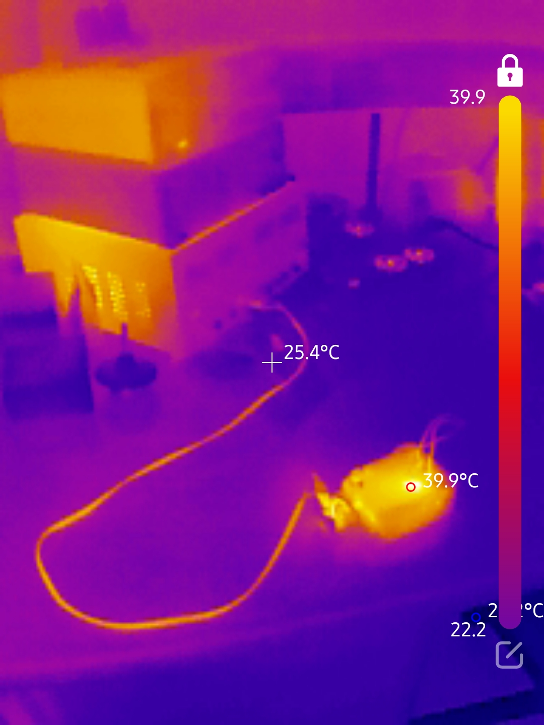
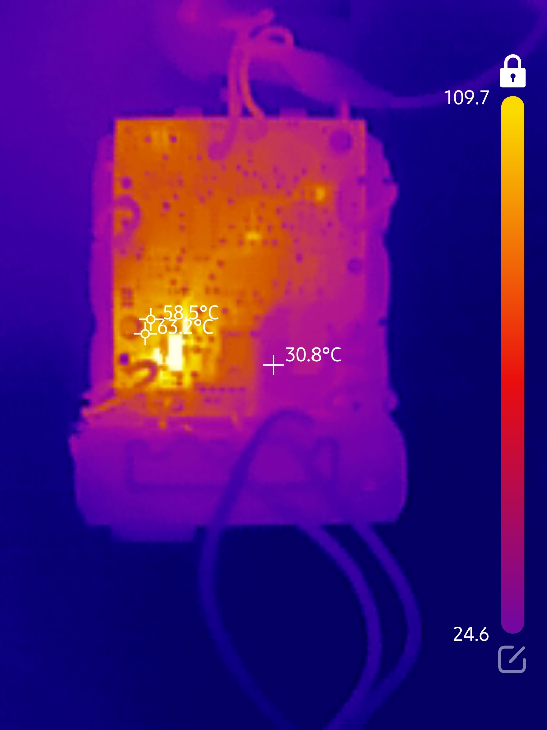
Sample Photos
Battery pack charging shown with a heated cable and packCharging PCB board with heated IC
Video
Thermal camera in electronic repairs
More specifically, thermal cameras can be a useful tool in electronics repair for troubleshooting and identifying issues. Here’s how you can use a thermal camera in the electronics repair process:
Power off the device: Before using a thermal camera, make sure the device is powered off and disconnected from any power source. This is important for safety reasons and to get accurate thermal readings without interference from active components.
Prepare the thermal camera: Ensure that your thermal camera is calibrated and ready for use according to the manufacturer’s instructions. Set the appropriate temperature range and adjust the camera settings if necessary.
Scan the device: With the thermal camera powered on, scan the device or circuit board. Look for any areas that show significant temperature variations. Hotspots or areas that appear unusually hot or cool compared to the surrounding components can indicate potential issues.
Identify overheating components: Pay attention to components that are generating excessive heat. These components may indicate a problem such as a faulty part, inadequate cooling, or excessive power dissipation. Thermal imaging can help pinpoint the exact location of the heat source.
Check for thermal anomalies: Look for temperature variations across different parts of the circuit board or device. Inconsistent temperatures may indicate poor electrical connections, shorts, or other faults. Thermal imaging can help identify these anomalies, guiding your repair efforts.
Assess cooling mechanisms: Evaluate the effectiveness of cooling mechanisms such as heat sinks, fans, or thermal pads. Use the thermal camera to check for proper heat dissipation and ensure that heat-sensitive components are adequately cooled.
Compare thermal patterns: If you have access to a known working device or a reference board, you can compare its thermal patterns to the device you’re repairing. This can help identify any discrepancies and give you a clearer idea of potential problem areas.
Document and analyze: Capture images or videos with the thermal camera to document the thermal patterns and areas of concern. Analyze the captured data to gain insights into the nature of the problem and assist in the repair process.
Purchase
The thermal camera comes in two versions, for Android and for iOS. If you are interested in purchasing the TOPDON TC001 for Android, visit this Amazon link. If you want the TOPDON TC002 iOS version then follow this Amazon link.
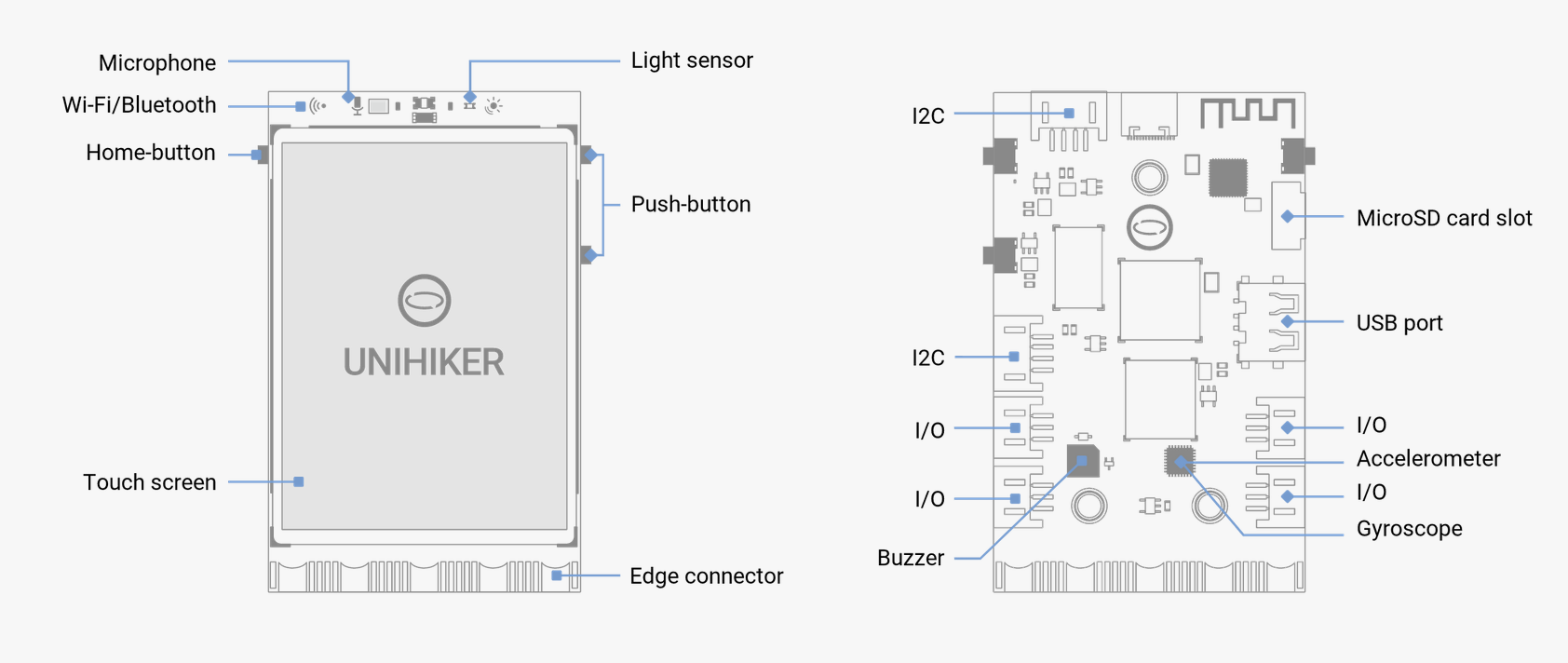
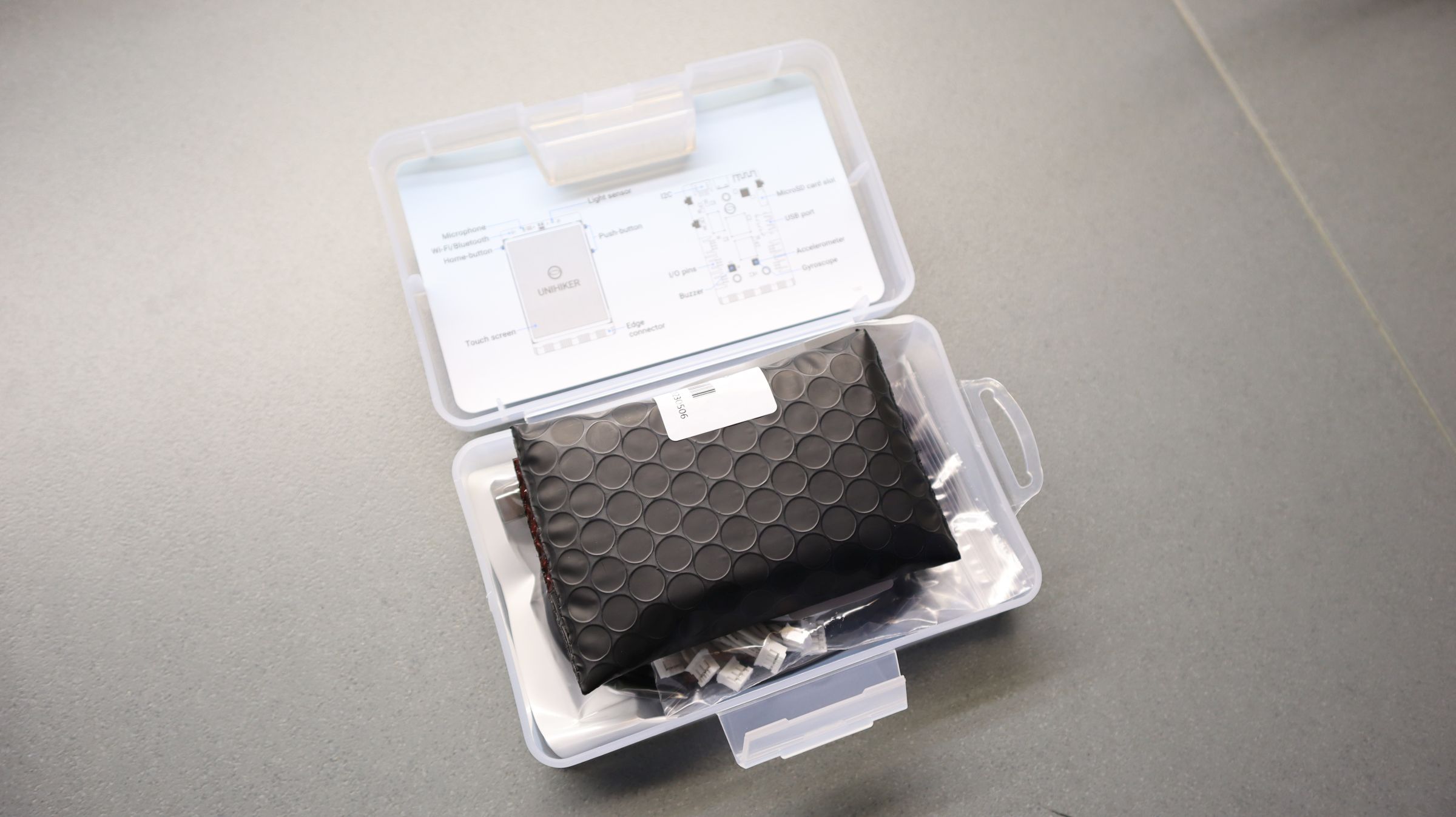
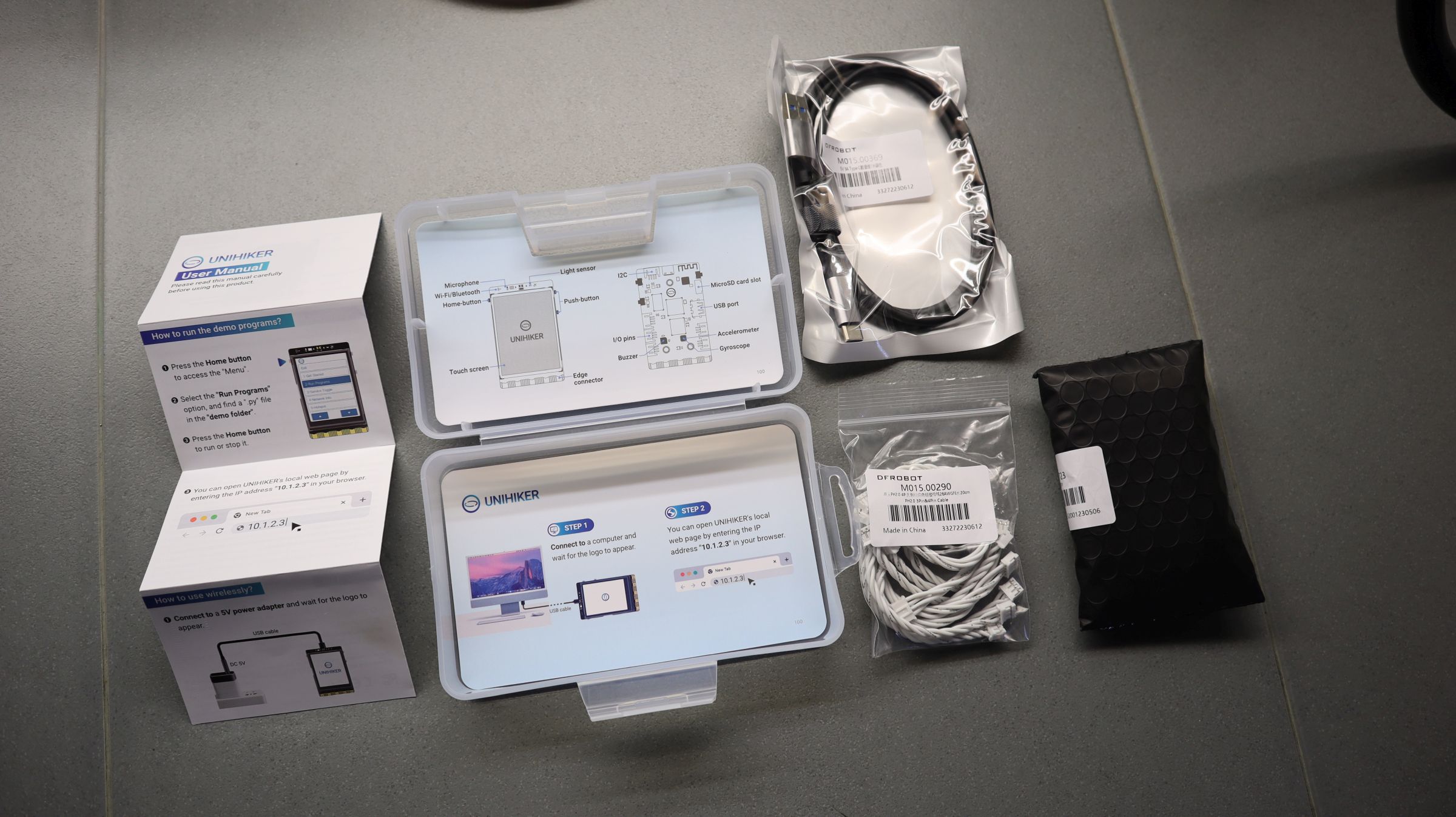
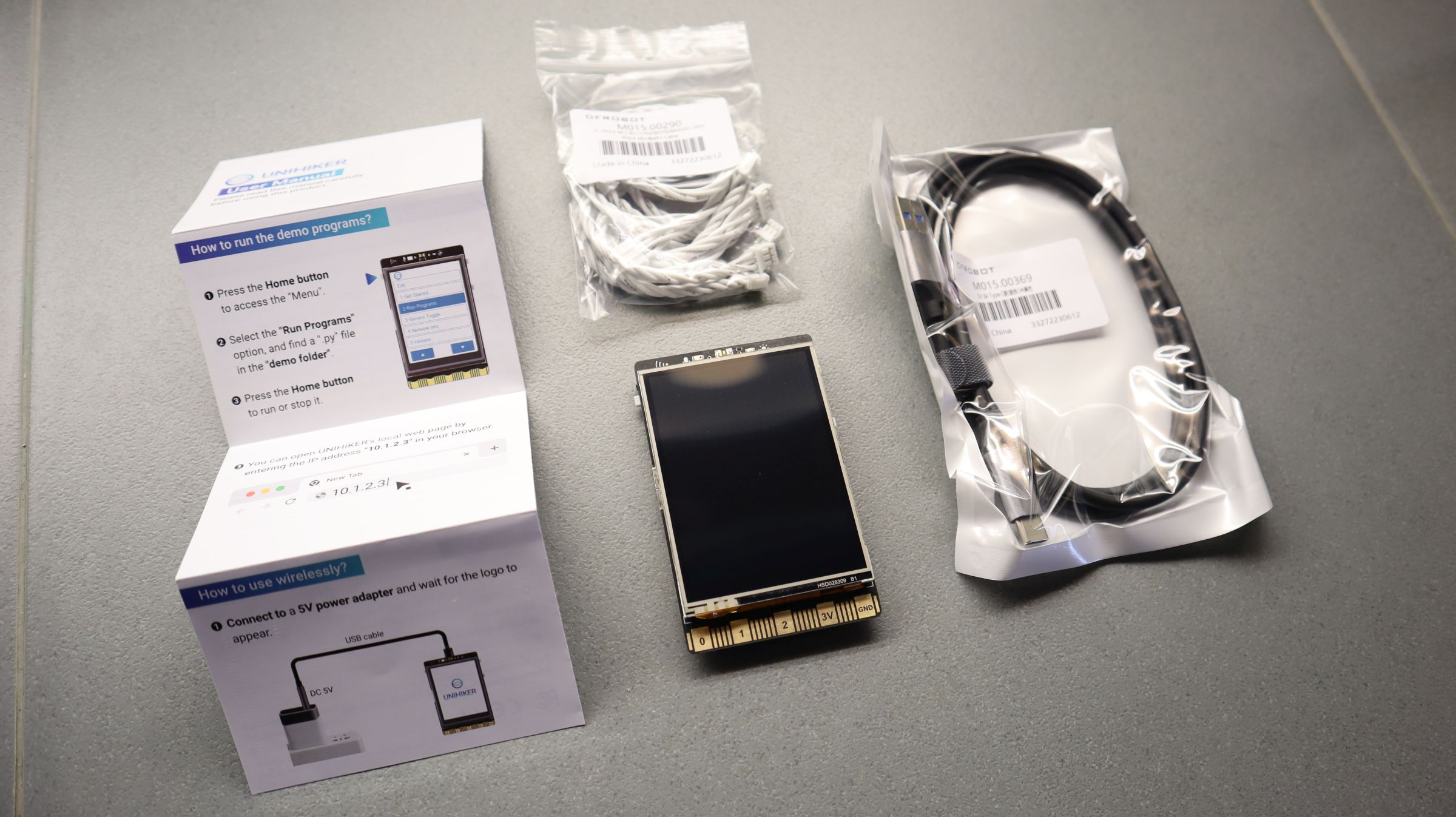
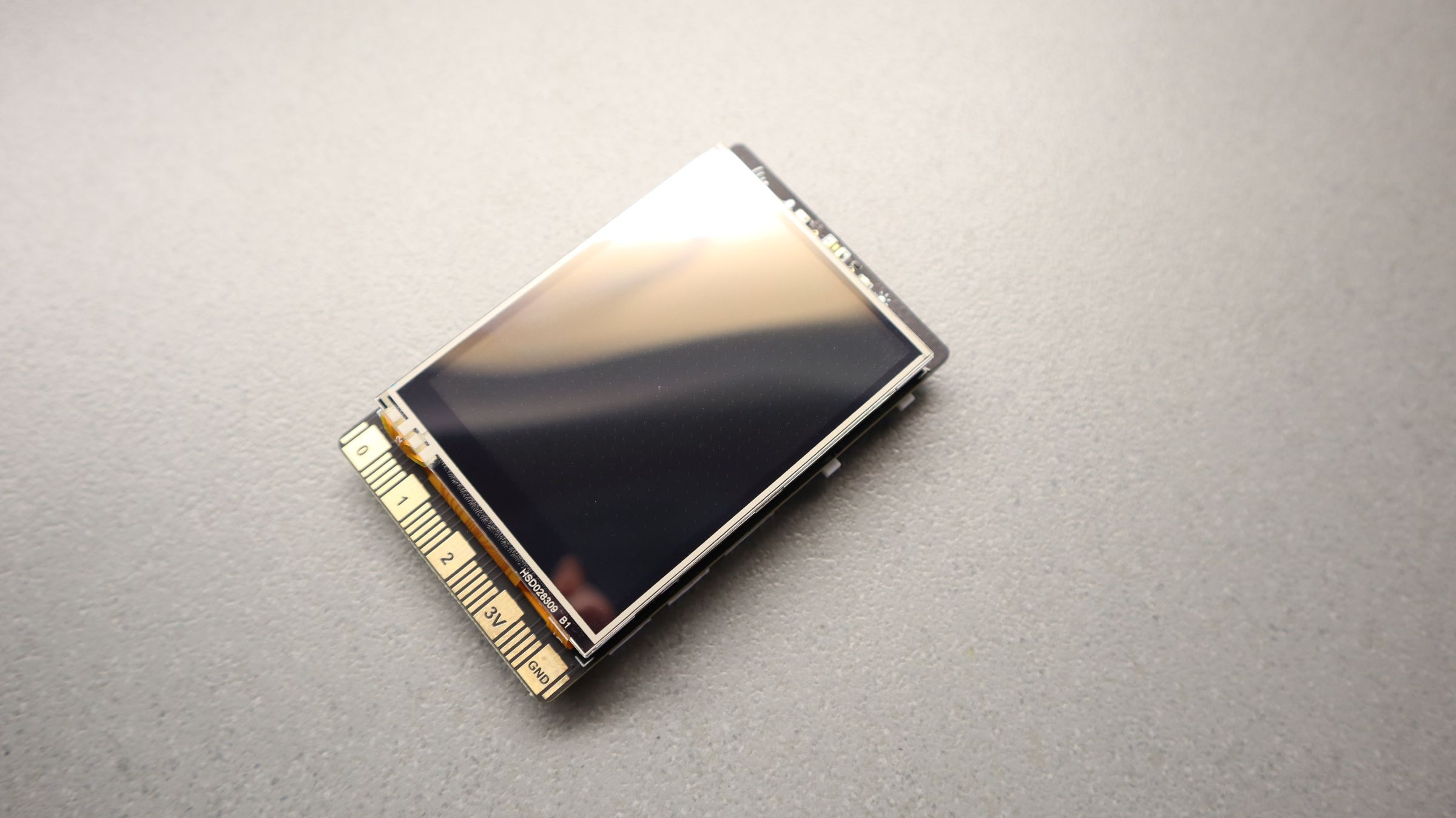
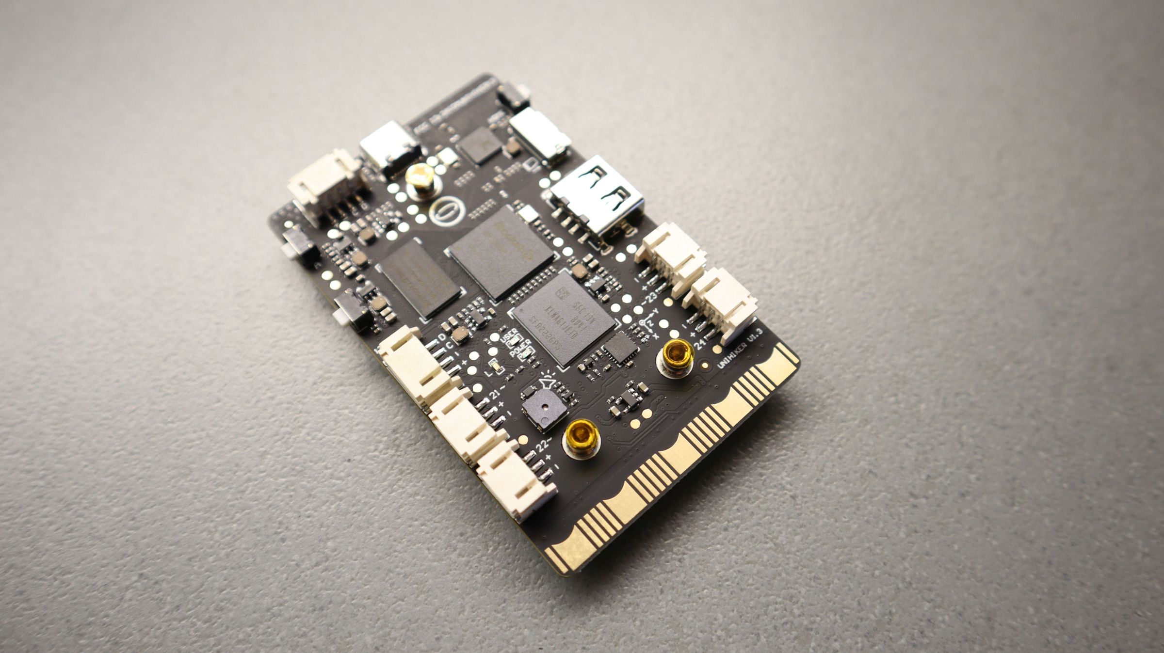
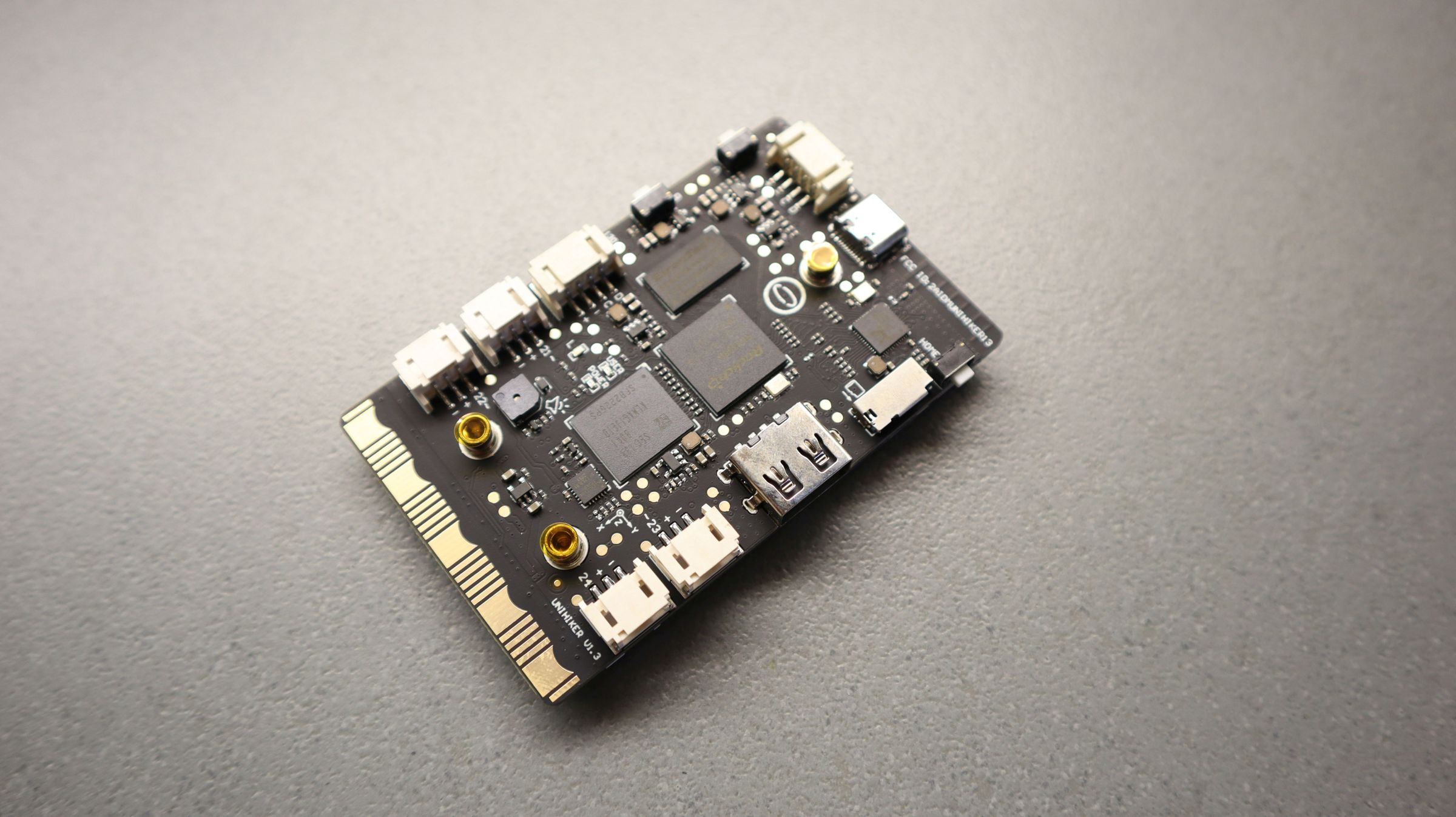
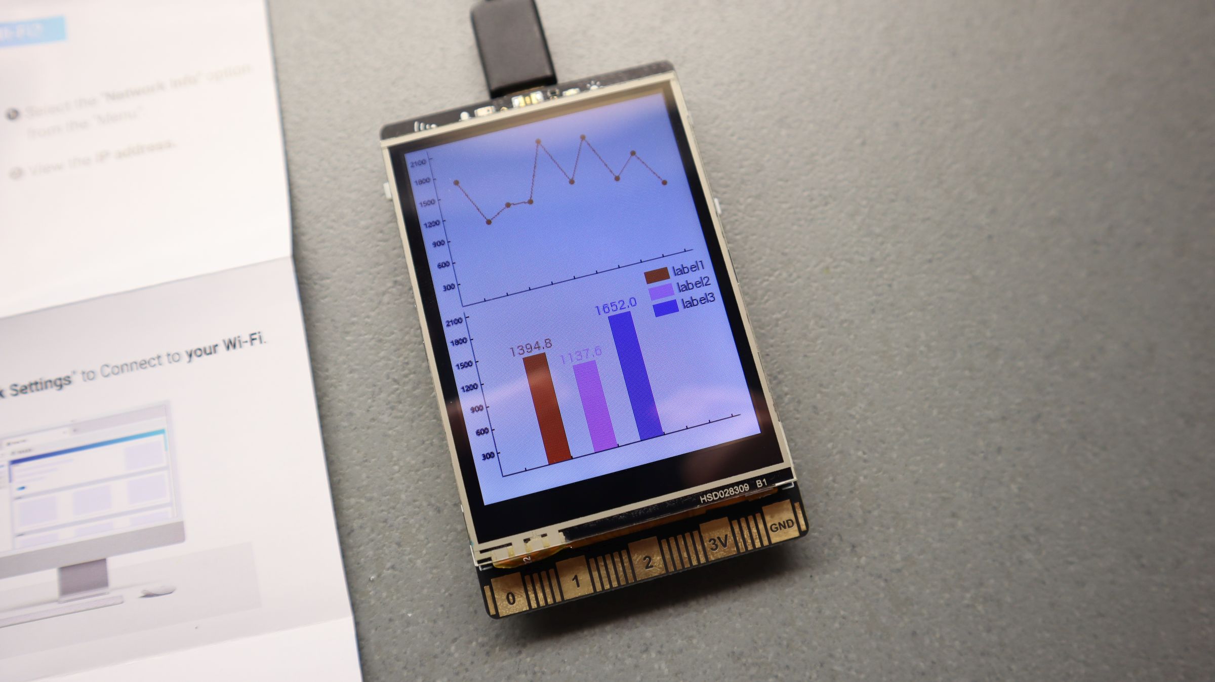
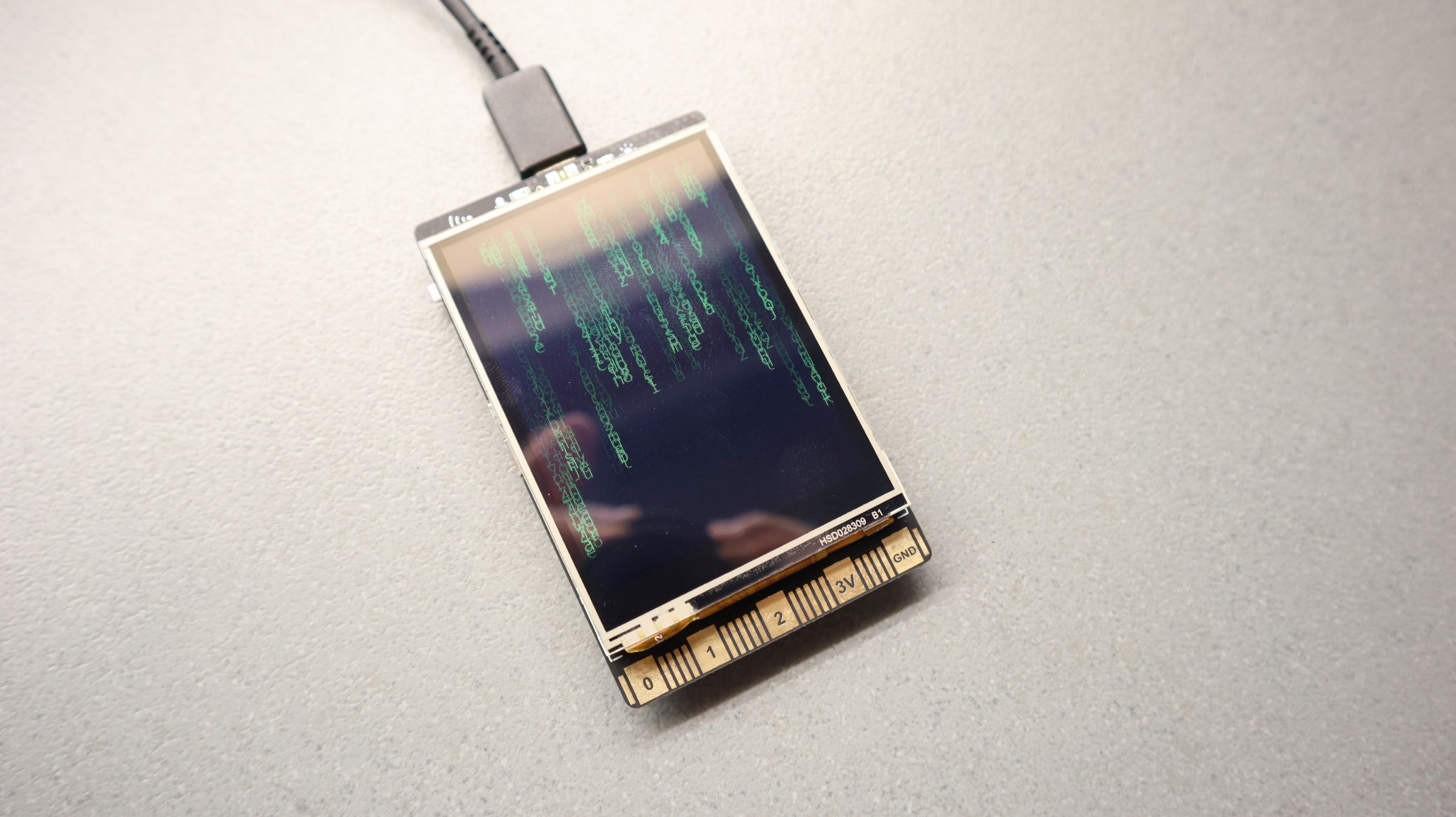
DFRobot, a leading provider of open-source hardware and robotics solutions, has recently launched the latest addition to its long list of single-board computers, called Unihiker. This hardware device is equipped with a built-in 2.8-inch touchscreen and offers a range of features that make it a powerful tool for IoT development and digital multimedia applications. The board is based on Quad-Core ARM Cortex-A35, up to 1.2GHz Rockchip RK3308 with 512MB of RAM, 16GB of flash, and running Debian OS.
Features of Unihiker microcomputer
The Unihiker single-board computer attracts a large community of embedded developers because of its main feature, the built-in 2.8-inch touchscreen. This compact display provides an intuitive interface for users to interact with the device and access various functionalities. With the built-in IoT service, Unihiker allows users to store data through the MQTT protocol and access real-time data via a web browser. This feature enables efficient connectivity and data management, making Unihiker an ideal choice for IoT projects and applications.
Unihiker comes with a rich interface, providing a range of connectivity options for enhanced adaptability. It includes a built-in microphone, enabling audio input for applications requiring voice interaction. The Wi-Fi and Bluetooth capabilities ensure robust wireless connectivity, allowing Unihiker to connect to other devices or networks. Additionally, the light sensor offers enhanced environmental awareness, enabling Unihiker to respond to changes in lighting conditions intelligently.
The push button provides a physical input option, while the edge connector allows for easy expansion and integration of external modules. Furthermore, Unihiker supports the I2C serial communication protocol, enabling easy interfacing with other devices and components.
Onboard system-on-chip
The Unihiker hardware platform is powered by the popular Rockchip RK3308 system-on-chip (SoC). The RK3308 is a high-performance quad-core application processor designed specifically for intelligent voice interaction, audio input/output processing, and other digital multimedia applications. With its powerful processing capabilities, this SoC ensures smooth and efficient performance, enabling users to easily develop and execute resource-intensive tasks.
Unihiker, with its compact size and comprehensive set of features, is a single-board computer suitable for a wide range of IoT projects and applications. Whether you are a hobbyist, a student, or a professional developer, Unihiker offers a user-friendly and flexible platform for bringing your ideas to life.
Port: USB Type-C, USB-A, MicroSD, Gravity 3pin/4pin port, Edge connector
Power: 5V 2A for USB Type-C
Size : 51.6mm x 83mm x 13mm
Software compatibility
Importantly, Unihiker is designed for entry-level embedded developers with its ease of coding. The manufacturer gives users the flexibility of programming from a computer, an iPad, or even a phone. Unihiker offers versatile options to suit your coding preferences. It also supports Hotspot functionality, allowing you to code and interact with the device from anywhere wirelessly. Unihiker supports popular coding software, including VS Code, Mind+, and Node-Red, making it accessible to both beginners and experienced developers.
Unihiker offers a built-in Jupyter Notebook, a popular browser-based programming environment. To further enhance the development experience, it comes with the integrated PinPong control library. This library allows developers to directly control the onboard sensors as well as hundreds of connected sensors and actuators using the popular Python programming language. With this level of control, developers can create interactive and responsive projects that leverage the full potential of the hardware capabilities.
How to program a Unihiker single-board computer?
To wirelessly program Unihiker, the first step is to connect it to a Wi-Fi network. This can be done by either connecting Unihiker to a router or by utilizing a mobile phone hotspot. It is important to note that when connecting to a Wi-Fi network, Unihiker operates on the 2.4GHz frequency, so it is crucial to ensure that the Wi-Fi network being used is compatible with this frequency.
Once Unihiker is connected to the Wi-Fi network, users can connect their programming devices, such as a computer, tablet, or smartphone, to the same Wi-Fi hotspot. This allows the programming devices to establish a connection with Unihiker over the network.
To initiate the programming process, users need to enter the IP address of Unihiker in the programming environment they are using. This IP address serves as the identifier to establish communication between the programming device and Unihiker. By entering the IP address, users can establish a connection and start programming Unihiker wirelessly.
The Unihiker single-board computer is available for purchase on the DFRobot website for $68.00 USD. With its affordable price point and powerful capabilities, users can explore the capabilities of Unihiker.
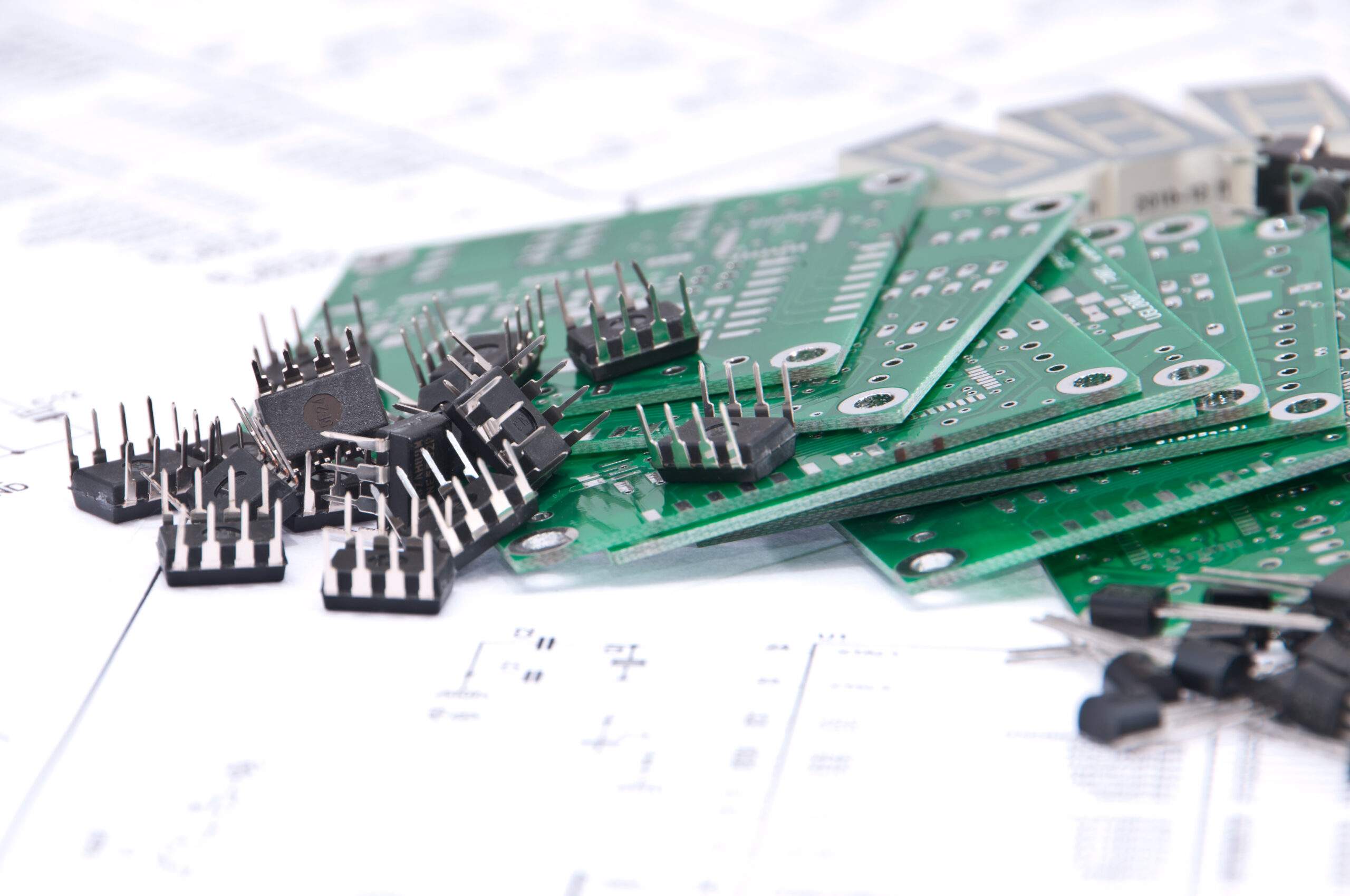
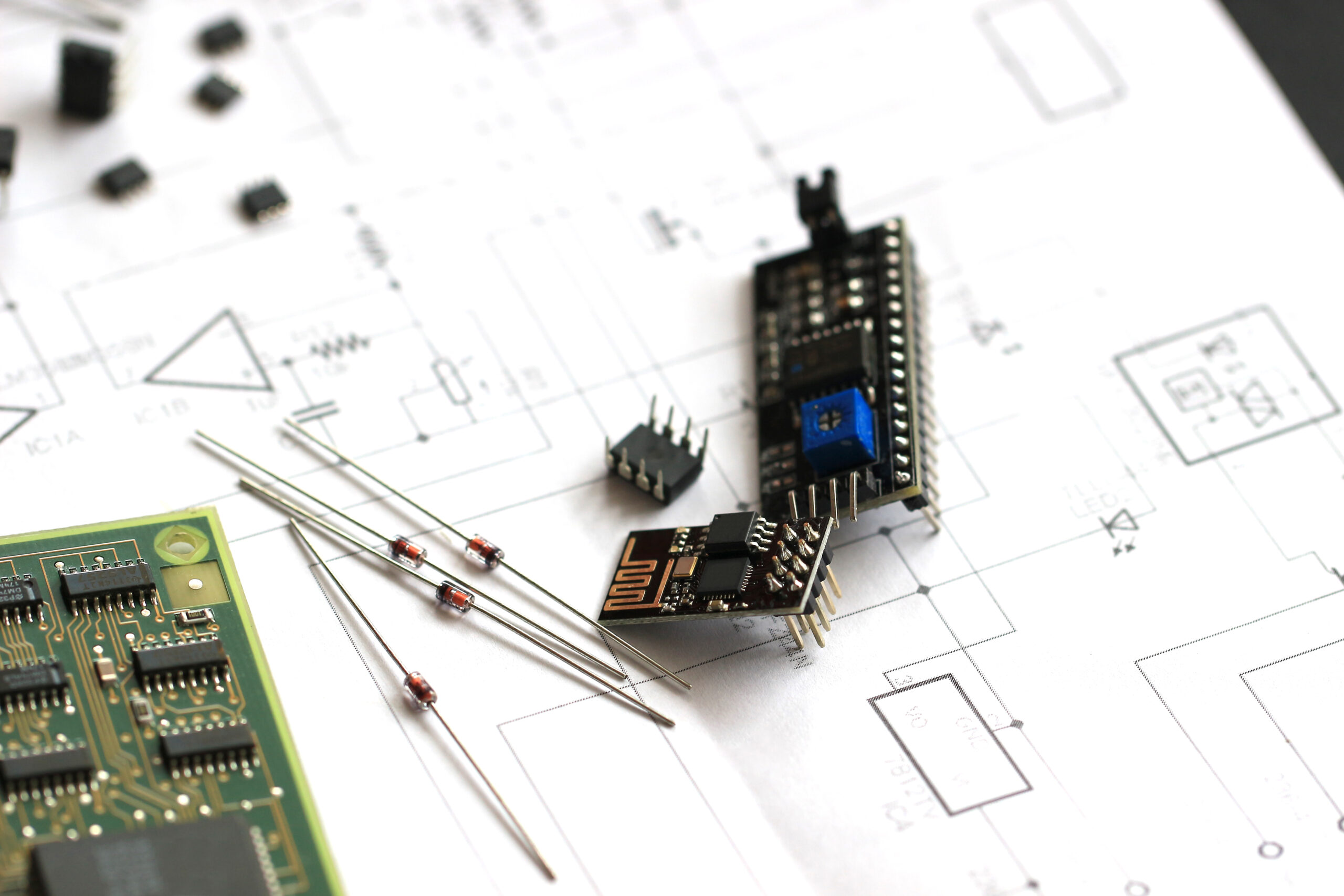
Electronic components play a crucial role in modern technology and are the building blocks of electronic devices. They are essential for the functioning of various electronic systems, from consumer electronics like smartphones and computers to complex industrial machinery and medical equipment. The importance of electronic components can be understood from the following perspectives:
Functionality: Electronic components enable the desired functions and operations of electronic devices. Each component serves a specific purpose, such as amplifying signals, storing data, converting energy, or controlling the flow of electricity. They work together in integrated circuits and systems to perform tasks efficiently and reliably.
Connectivity and Communication: Components like transistors, capacitors, and resistors facilitate the transmission and processing of signals, enabling communication between different electronic devices. These components ensure that data, audio, and video signals can be transmitted accurately and at high speeds, enabling seamless connectivity and information exchange.
Miniaturization and Portability: Electronic components have significantly contributed to the miniaturization and portability of electronic devices. Advances in component technology have allowed devices to become smaller, lighter, and more energy-efficient. This has led to the development of portable devices like smartphones, laptops, and wearable gadgets that have become an integral part of our daily lives.
Performance and Efficiency: High-quality electronic components contribute to the performance and efficiency of electronic systems. Components with improved specifications, such as higher processing speeds, lower power consumption, and increased storage capacity, enhance the overall functionality and user experience of electronic devices. They also enable energy-efficient designs, reducing power consumption and environmental impact.
Innovationand Advancement: Electronic components drive innovation and advancement in various industries. New and improved components enable the development of cutting-edge technologies, such as artificial intelligence, virtual reality, autonomous vehicles, renewable energy systems, and medical advancements. Components with enhanced capabilities open up new possibilities and push the boundaries of what is technologically achievable.
So how does an engineer choose the right online store?
Large inventory: As an engineer, having access to various components is crucial. Find an online store with a large inventory to meet the needs of different industries and applications. The availability of specialized components and hard-to-find parts can be a significant advantage.②
Technical Specifications: Make sure that the online store provides detailed technical specifications and data sheets for the components it offers. This is critical for engineers who need specific parameters to meet project requirements and compatibility.
Reliability and authenticity: Engineers give priority to the quality and authenticity of components. Reliable components reduce the possibility of system failure, downtime, and safety hazards, and can ensure long-term functionality while reducing maintenance costs. This can be judged by looking for certifications and customer reviews that demonstrate the authenticity and reliability of components.
Fast delivery and support: Timeliness is critical for engineers working under tight deadlines. Choose an online store that offers fast shipping options, reliable delivery, and tracking. Also, priority is given to stores that offer efficient technical support for any project-specific queries or challenges.
Electronic Components Online Store Ranking
Digi-Key Electronics is an American distributor of electronic components, established in 1972, offering a wide variety of electronic components, including semiconductors, capacitors, connectors, sensors, etc., offering more than 11 million items from thousands of manufacturers’ Extensive catalog of products. 99.9% of orders ship same day, available 24/7.
Mouser Electronics is a global distributor of semiconductors and electronic components, founded in 1964, the site features products from 1,200 manufacturer brands, with access to 6.8 million products and data sheets. Its global distribution centers process orders 24/7.
Arrow Electronics is one of the largest distributors of electronic components in the world. Founded in 1935, the company specializes in distribution and value-added services related to electronic components and computer products. For same-day shipping, orders must be placed by 9 pm ET, Monday – Friday. The cut-off time for all ground shipments is 11:00 PM ET, and orders placed after the cut-off time will ship the next business day.
Win Source is a global distributor of electronic components, established in 1999, offering a wide range of commonly used components such as semiconductors, passive components, connectors, sensors, etc., as well as many shortage and obsolete parts. With 1 million+ product inventory from 3000+ suppliers, 24-hour delivery, and 365-day quality assurance. Passed the ISO14001, ISO9001, and other quality inspection systems, and provide free samples for trial use.
Farnellis a well-known distributor of electronic components, products, and solutions, established in 1939. With about 2000 manufacturers products. Access global inventory with delivery speeds of up to 2-4 days.
Rutronikis the world’s leading distributor of electronic components, embedded circuit boards, and systems. Provide efficient order processing, reliable shipping, and localized customer support. Founded in 1973
Adafruit Industries offers a wide range of products including Arduino, sensors, displays, and other electronic components. Free shipping to the continental US on orders over $200. Founded in 2005
SparkFun Electronics is committed to providing innovative electronic components, development tools, and educational resources for makers, hobbyists, and professionals. Free shipping is available on orders of $100 or more with shipping within the US. Founded in 2003
Jameco Electronics, a leading distributor of electronic components founded in 1974, offers over 30,000 of the industry’s most popular name-brand components with free shipping on orders over $150.
Angliais the UK’s leading independent authorized distributor of semiconductor, optoelectronic, passive, and electromechanical components. Established in 1972, stock over 2 billion components from over 1.3 million product lines in the UK, available for same-day dispatch.
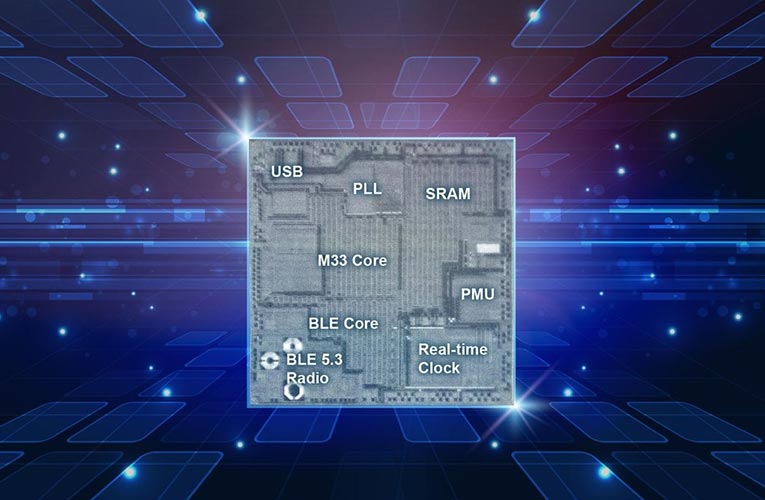
Renesas has recently announced that they will be introducing their first MCU on the new 22nm node. This MCU will be an expansion of the RA 32-bit Arm Cortex-M family and will be specifically designed for wireless applications. It will incorporate software-defined radio and provide support for Bluetooth 5.3 low energy, including in-field upgrades for new wireless capabilities. With this new device, developers will only need one MCU to accommodate all previous Bluetooth specifications, such as Bluetooth 5.1 Angle of Arrival/Angle of Departure and Bluetooth 5.2 isochronous channels for low-power stereo audio transmission.
Renesas anticipates significant improvements in performance and power consumption due to the migration to the smaller 22nm process node. They expect lower power consumption by utilizing reduced core voltages. Additionally, the company claims that the smaller die area of the MCU will enable the integration of memory and peripherals, resulting in smaller chips with enhanced functionality. The 22nm device is currently being sampled by Renesas, and the company plans to officially launch it in the fourth quarter of 2023.
According to Renesas’ Roger Wendelken during the sampling phase, Renesas’ dominance in the field of microcontroller units (MCUs) stems from their extensive range of products and expertise in manufacturing process technologies. Wendelken expresses satisfaction in introducing the initial 22nm product development within the RA MCU family, which will serve as a foundation for future-generation devices that enable customers to safeguard their designs and ensure long-term availability. Renesas remains dedicated to delivering top-notch performance, user-friendly experiences, and the most up-to-date features in the market. This milestone signifies just the initial step in their progress.
In the realm of semiconductor manufacturing, nanometers have become a means of measuring and distinguishing between different process nodes. Initially, it referred to the size of specific features, then to the smallest gap between features, and now it serves as a broad indicator for differentiating next-generation process nodes from previous ones. High-frequency application processors, such as those produced by Intel or AMD, are currently exploring single-digit nanometer process nodes at the cutting edge. However, microcontrollers, which require fewer transistors than high-performance processors, have traditionally opted for established and cost-effective double- or triple-digit process nodes.
Renesas’ announcement of a microcontroller built on a 22nm process node holds significance due to its context. Intel had previously utilized the 22nm process node in 2012 for its Ivy Bridge chip family before transitioning to 14nm for Broadwell in 2014. In the realm of microcontrollers, the utilization of a 22nm process node represents an advanced technology. This advancement enables Renesas to incorporate a greater number of components within a given area. Renesas has capitalized on this expanded capacity by integrating a software-defined radio (SDR) into the chip. This SDR empowers Bluetooth 5.3 Low Energy (BLE) connectivity, including features like direction-finding and low-power audio capabilities at launch. Moreover, the chip can be upgraded post-release to support new radio protocols and standards as needed.
The transition to a 22nm node not only brings advantages in terms of size reduction but also offers opportunities for improved efficiency. These benefits can be leveraged to achieve either enhanced performance with the same power consumption or reduced power consumption for the same level of performance. Alternatively, a balanced combination of both can be achieved. While Renesas has not yet disclosed complete specifications for the part, including frequency and power requirements, the utilization of the 22nm node holds the potential for significant advancements in these areas.
Renesas is currently providing samples of the 22nm RA-family chips to specific customers for testing and evaluation. The company intends to make the chips widely available by the end of the year. If interested in requesting a sample, individuals or organizations can reach out to their local sales office for further information and details.