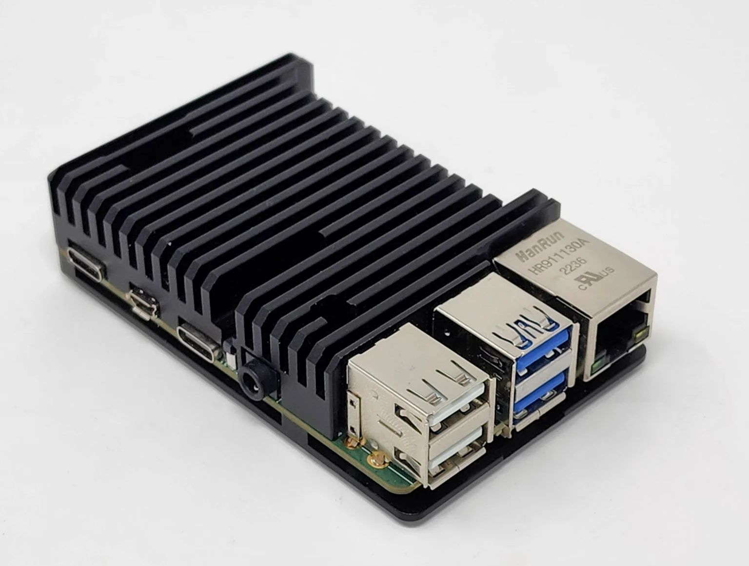
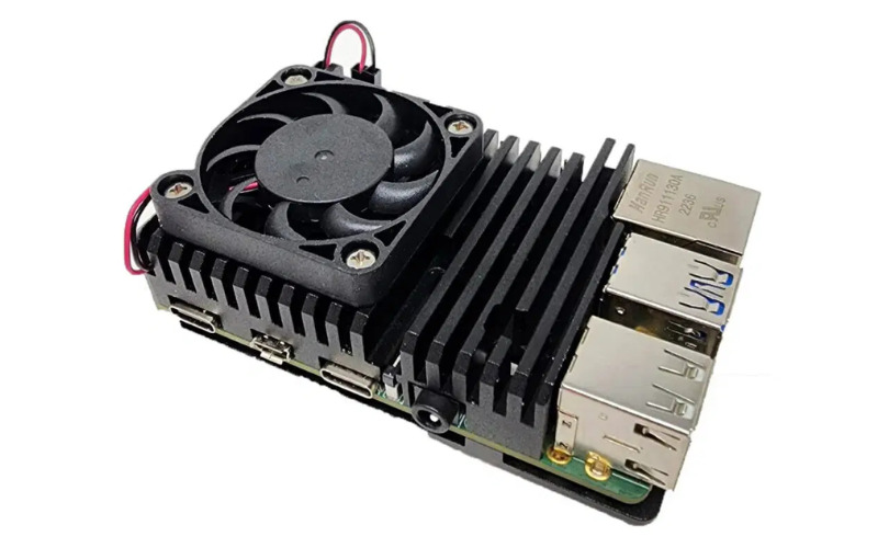
The Indiedroid Nova single-board computer is a powerful hardware platform that has a compact form factor, similar to the Raspberry Pi 4B. The device comes with triple display support, including 8K, 4K, and 4K output. It enables the customer to connect dual monitors, along with a DSI display, offering up to four times the resolution of 4K.
The Indiedroid Nova is powered by the Rockchip RK3588S octa-core processor. This SoC is assumed to be a cost-optimized version of the RK3588, specially designed for graphics-intensive applications. The RK3588S features four Cortex-A76 cores running at speeds of up to 2.2-2.4 GHz, along with four Cortex-A55 cores clocked at up to 1.8 GHz. This combination of high-performance and power-efficient cores ensures smooth multitasking and responsive performance.
Driving the graphics capabilities of the Indiedroid Nova is the Arm Mali-G610 GPU. This GPU is equipped with OpenGL ES 3.2, OpenCL 2.2, and Vulkan 1.2 support, enabling it to render high-quality graphics with incredible detail. Even if the customer intends to work with complex visualizations, the Mali-G610 GPU delivers exceptional visuals in resolutions up to 8K.
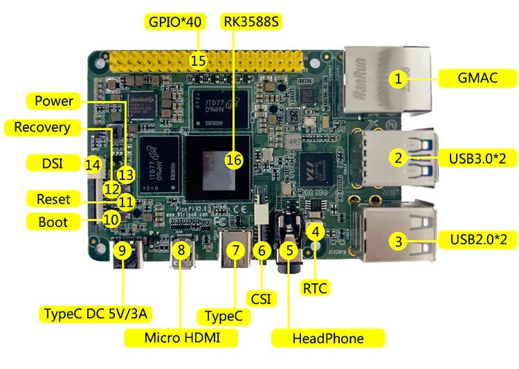
Specifications of Indiedroid Nova single-board computer
SoC: Rockchip RK3588S
CPU: Octa-core processor, 4x Arm Cortex-A75 and 4x Arm Cortex-A55
GPU: Arm Mali-G610
VPU: 8Kp60 video decoder for H.265/AVS2/VP9/H.264/AV1 codecs
NPU: AI Acceleration at 6 trillion operations per second
Memory: 4GB, 8GB, or 16GB LPDDR4x
Storage: eMMC 5.1 flash module connector to add 8GB, 16GB, 32GB, 64GB, or 128GB module
Video output: 1x micro-HDMI 2.1 port, DisplayPort via USB Type-C, and 4-lane MIPI DSI connector
Camera: MIPI CSI connector
Audio: 3.5mm earphone jack
USB: 1x USB Type-C port, 2x USB 3.0 Type-A ports, 2x USB 2.0 Type-A ports
Expansion: 40-pin Raspberry Pi compatible GPIO header
Power supply: 5V/3A via USB Type-C port
Dimensions: 85×56 mm
The manufacturer ships the Indiedroid Nova single-board computer pre-flashed with the Armbian Ubuntu operating system on the eMMC. This ensures that you can start using the SBC right out of the box. Each Nova unit is thoroughly tested before shipping, guaranteeing that all components are in working order.
Indiedroid Nova is available in many configurations. The entry-level variant offers 8GB of RAM and 32GB of flash storage, priced at $164.95 USD. If you require even more power and storage capacity, the top-tier version provides 16GB of RAM and 64GB of flash storage, available at $224.95 USD. With these options, you can choose the configuration that best suits your application needs.
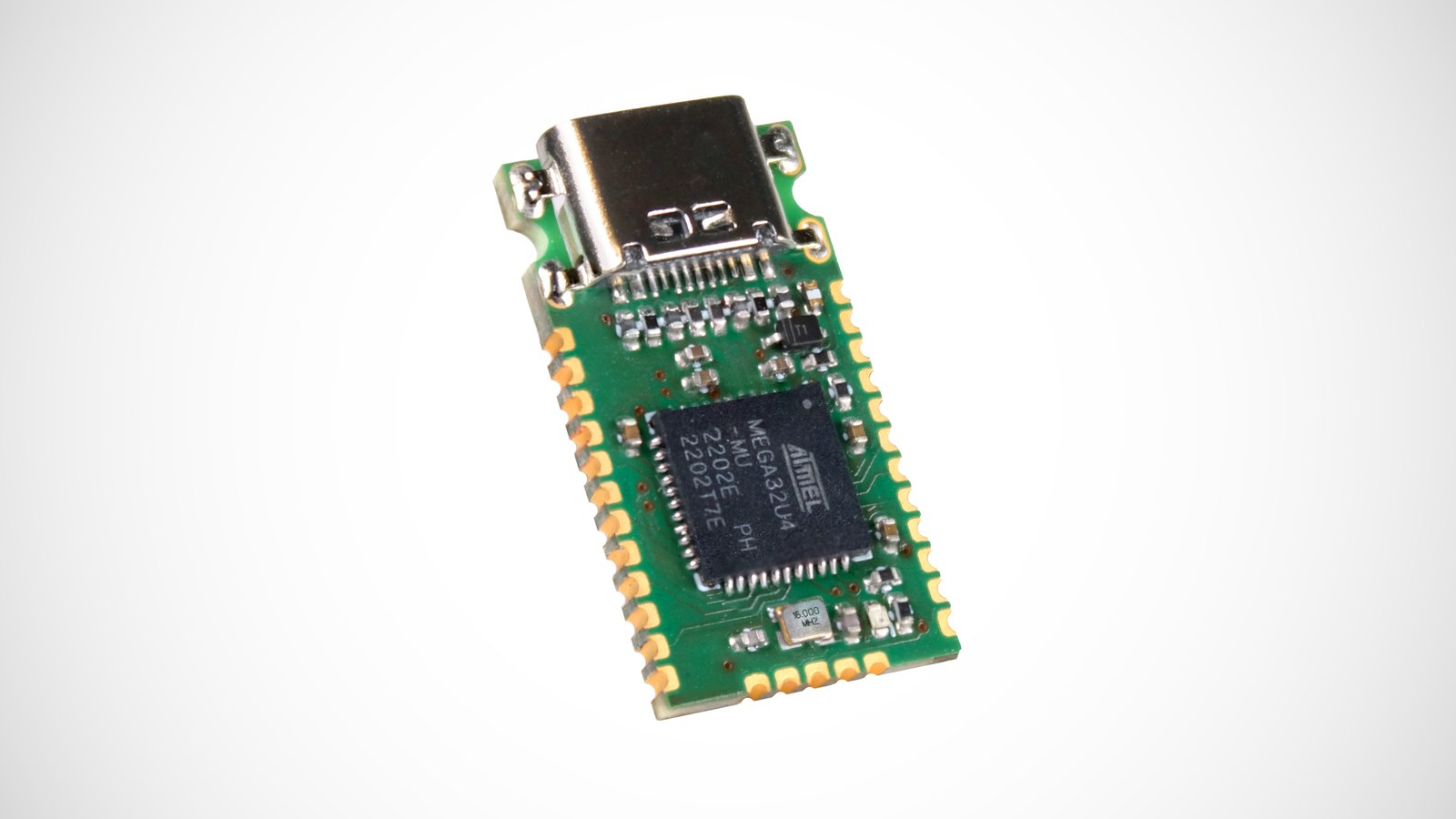
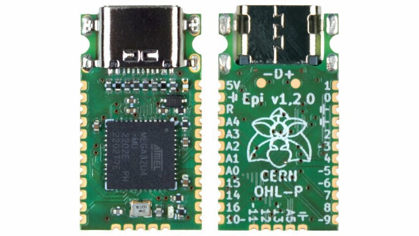
The Epi 32U4 is an open hardware device designed by Ping Hobbyelektronik, offering a powerful solution in an extremely compact form factor. This Arduino-compatible ATmega32U4 USB Type-C development board allows for easy integration into a wide range of projects. Customers can choose to solder it directly onto a PCB or opt for a less permanent mounting solution using the included headers.
At the heart of the Epi 32U4 is the ATmega32U4, a low-power Microchip 8-bit AVR RISC-based microcontroller. Its unique architecture enables the execution of powerful instructions in a single clock cycle. This efficiency translates into impressive throughput, approaching one million instructions per second (MIPS) per megahertz (MHz). With this capability, users can strike an optimal balance between power consumption and processing speed, tailoring their projects to specific performance requirements.
Specifications of Epi 32U4:
Microcontroller: ATmega32U4 with a 16MHz crystal
USB: Type-C port
Input/output interfaces: 24x
LED: Pin 13
Surge protection: ESD and surge protection on USB data lines and power input
Operating voltage: Runs at 4.5 to 5.5 V for the 16 MHz version, down to 2.7 V at 8 MHz
Dimensions: 22.75×12.75 mm
The board does not have a dedicated LED for RX, TX, and power status. Instead, the Epi 32U4 includes a single LED on pin 13, primarily intended for testing purposes.
Interestingly, the Epi 32U4 has the ability to function as a USB device. This feature makes it particularly well-suited for projects such as compact keyboards, where its small size is an advantage. The inclusion of a USB Type-C connector ensures that designs are compatible with the latest standards. Furthermore, the Epi 32U4 offers more available IO ports compared to a standard Pro Micro, making it a suitable choice for projects where space is not a limiting factor.
The Epi 32U4 is currently seeking crowd support on CrowdSupply with a raised amount of $763 as of writing. Interested individuals can contribute to the project and secure their own board at a purchase price of $25. Interested developers can also contribute to the ongoing development of Epi 32U4 on the official GitHub page.
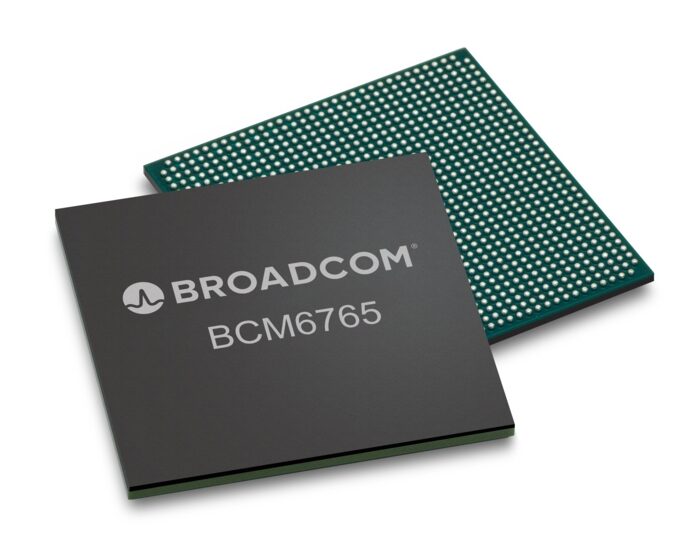
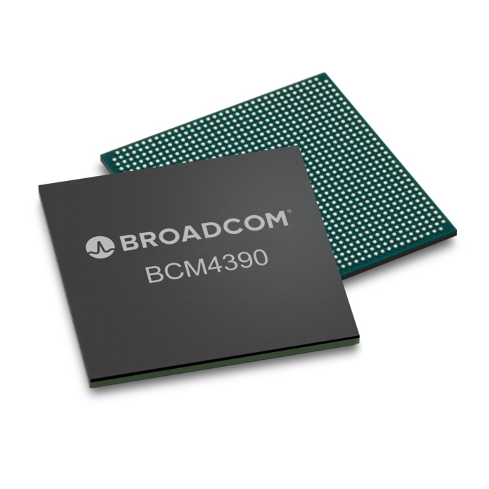
Broadcom, a leading semiconductor company, has recently unveiled three of its second-generation Wi-Fi 7 chip range, designed for wireless connectivity in various sectors. These chips support Wi-Fi 7 along with integrated Bluetooth Low Energy (BLE) and Zigbee, Thread, and Matter protocols. The company aims to equip developers with necessary wireless connectivity options to explore new possibilities for the Internet of Things (IoT) and other applications.
The first in line is the BCM6765, designed for residential access point chips to enable the mass-market production of Wi-Fi 7 access points and smart repeater solutions. The device uses 320 MHz 2-stream Wi-Fi operation to cater to a range of cost, form factor, and performance requirements, ensuring advanced connectivity for homes and businesses.
Another product to the portfolio is the BCM47722, an enterprise access point platform SoC, which features dual IoT radios that enable simultaneous operation for BLE, Zigbee, Thread, and Matter protocols. As the demand for IoT applications continues to rise in the enterprise Wi-Fi market, BCM47722 addresses this need by offering robust connectivity and optimized performance. When it comes to mobile devices, such as handheld devices, the BCM4390 fills in the gap with a low-power Wi-Fi, Bluetooth, and 802.15.4 combination device platform.
“Arcadyan is proud to expand our collaboration with Broadcom to build out our portfolio of Wi-Fi 7 solutions for the service provider market. Broadcom’s modular approach of Wi-Fi 7 solutions enables a full spectrum of residential gateways and extenders options which can be optimized for performance, form factor, and cost and gives us the flexibility to address our customers’ specific needs,” says Raymond Hsiung, vice president, Sales & Marketing at Arcadyan.
The BCM47722 includes an integrated quad-core Armv8 CPU and supports multi-link operation (MLO) with up to 3-link support on the SoC and SpeedBooster support. Moreover, it integrates dual radio Bluetooth Low-Energy, Thread, and Zigbee support, complying with IEEE, WFA Wi-Fi 7, and Automated Frequency Coordination (AFC) specifications, as well as the Bluetooth 5.4 standard and future draft specifications.
Broadcom is currently sampling its second-generation Wi-Fi 7 chips to early access partners and customers in various industries.
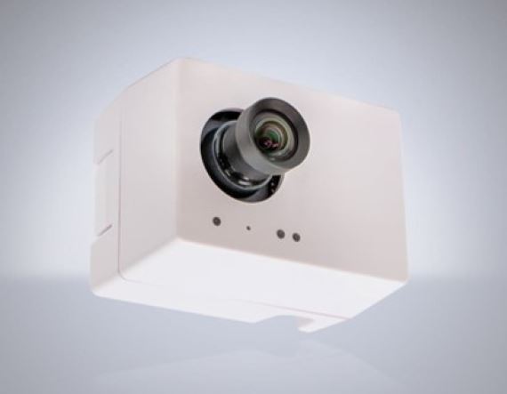
LUCID Vision Labs introduces the SENSAiZ SZP123S-001 smart camera, which is designed to work with the Sony IMX500 intelligent vision sensor and Sony’s innovative AITRIOS software platform. The smart camera is a compact and lightweight device that combines high performance with ease of integration. It features a built-in camera lens and an Ethernet PoE connection, making it easy to integrate into various applications, such as security systems, manufacturing processes, and robotic automation.
TheSony IMX500 intelligent vision sensor powers the SENSAiZ SZP123S-001. This sensor combines an image sensor with a powerful DSP and dedicated on-chip SRAM. This unique configuration enables high-speed edge AI processing. By eliminating the requirement for high-performance processors or external memory, the IMX500 makes devices more reliable and cost-effective to produce.
The IMX500 sensor has the ability to perform AI inference at the edge. This means that image data can be processed locally without the need for uploading to a cloud server. As a result, solutions powered by the IMX500 sensor experience lower latency and require less bandwidth and power compared to traditional vision systems. This efficiency opens up new possibilities across a wide range of visual applications.
The smart camera supports the Sony Aitrios software platform, which aims to bring image processing and AI analysis directly to the camera, eliminating the need for external processing or memory. Using Aitrios, users can easily deploy, evaluate, and iterate any neural network, enabling them to unlock the full potential of their intelligent vision systems. Sony’s AITRIOS software platform complements the capabilities of the smart camera solution by providing a comprehensive software solution for device management, AI development, and system integration
Sony Semiconductor Solutions recently made a strategic investment in Raspberry Limited to provide Aitrios, an edge computing platform deeper into the Raspberry Pi community. More information is in our previous blog post.
The LUCID Vision Labs SENSAiZ SZP123S-001 smart camera is currently on the market, priced at $335.
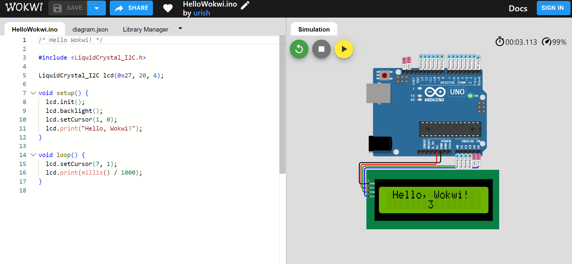
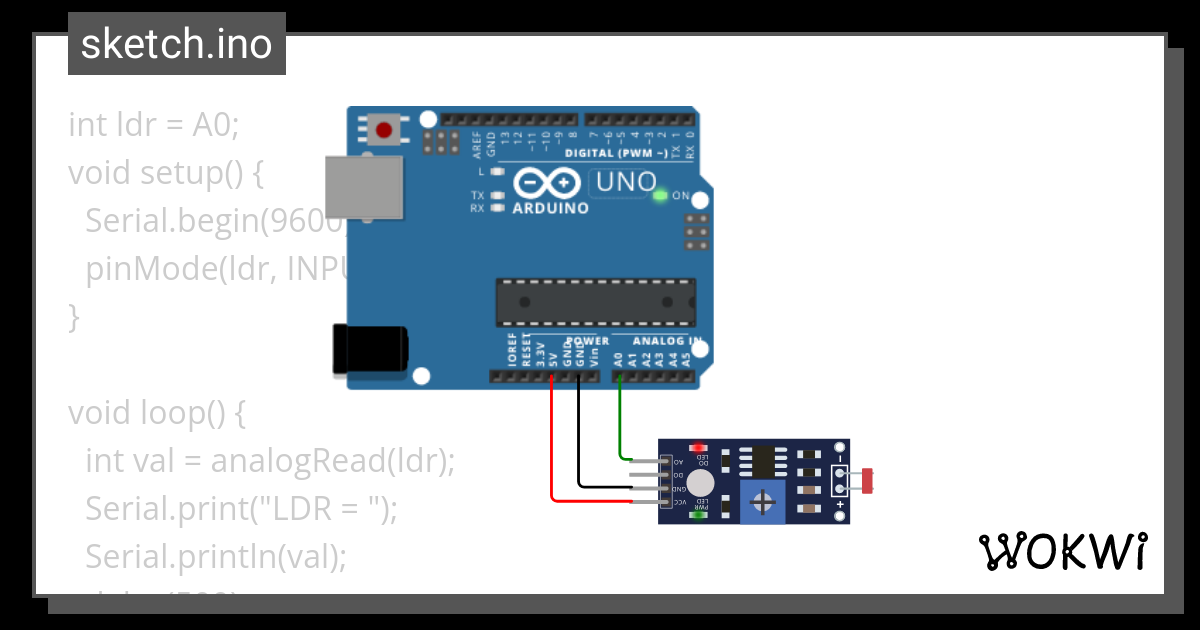
Wokwi is an innovative online simulator designed to cater to the needs of Arduino, Raspberry Pi Pico, and ESP32 enthusiasts. But the developers have not stopped there; you can also use this simulator for your custom boards. With Wokwi, you can start coding your next IoT project in seconds without waiting for physical components or downloading extensive software. This platform leverages the power of your browser, providing a seamless experience for programming and prototyping.
With Wokwi, it is easy to get assistance and feedback. It only takes you to share your Wokwi project to receive help and guidance from the community. Whether you are a beginner seeking support or an experienced developer looking to share your expertise, Wokwi creates a collaborative environment where learning becomes easy.
Wokwi also enables you to gain confidence in your code by separating hardware and software issues. This means you can focus on developing your programming skills without being affected by hardware limitations or connectivity concerns. By eliminating these barriers, Wokwi enables you to redefine your coding and create robust IoT projects.
Wokwi allows you to simulate Wi-Fi connectivity, enabling your virtual project to connect to the internet. Even if you are using MQTT, HTTP, NTP, or other network protocols in your project, Wowki supports them all. This opens up several possibilities for IoT projects that rely on internet connectivity.
The simulator also supports a virtual logic analyzer, enabling you to capture and analyze digital signals such as UART, I2C, and SPI. By providing this functionality, Wokwi facilitates in-depth debugging and analysis, enhancing your understanding of complex communication protocols.
For advanced users, Wokwi offers advanced debugging capabilities through integration with the GDB (GNU Debugger). This powerful feature caters to Arduino and Raspberry Pi Pico developers, providing them with a comprehensive debugging toolset to tackle complex projects.
Wokwi’s SD card simulation feature allows you to store and retrieve files and directories from your code. Moreover, club members can upload binary files, including images, further expanding the possibilities for creative projects and simulations.
The platform also has a Chips API, enabling users to create custom chips and parts that can be shared with the Wokwi community. This builds a collaborative environment where developers can exchange their innovation and push the boundaries of what can be achieved in the virtual simulator.
If you are interested in checking out the free-of-charge Wowki online simulator, head to the official website.
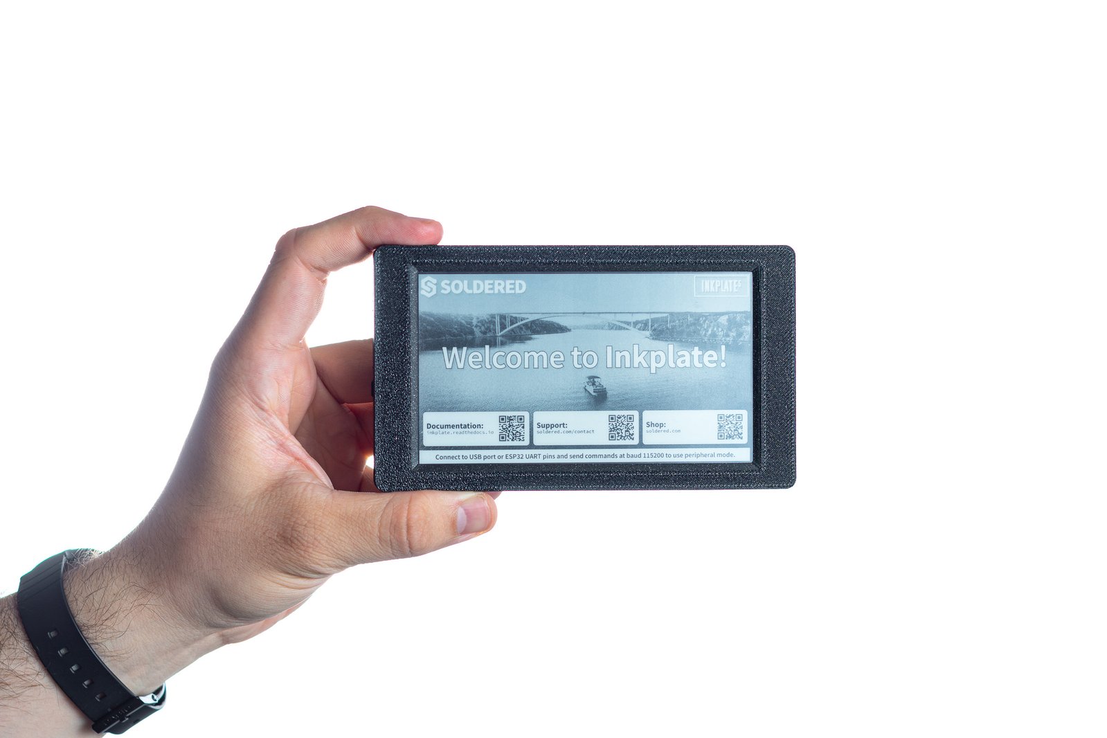
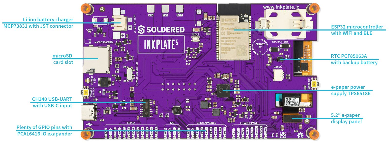
Inkplate 5 is an open hardware that innovates the e-paper displays offerings. With its 5.2-inch e-ink (e-paper) screen and fast refresh speed, this board offers an excellent solution for projects requiring low-power, high-quality visual displays. The manufacturer has designed the display module to support Arduino and MicroPython for easy customization.
At the core of the Inkplate 5 is its remarkable e-paper panel display. With a screen resolution of 960×540 pixels and support for black, white, and six shades of grey, the Inkplate 5 delivers sharp image quality that remains visible even under direct sunlight. What sets e-paper apart from traditional displays is its always-on feature, which means it consumes no power between screen updates. Moreover, the Inkplate 5 has an impressive refresh rate, performing a full refresh in as quick as 1.02 seconds and a partial refresh in a mere 0.19 seconds, equivalent to 5 frames per second.
The user interface of the Inkplate 5 is designed to be simple and user-friendly. The hardware is plug-and-play, making it incredibly easy to set up. Simply connect the device to your computer using the supplied USB cable, and it will start working without any complex configurations or setup processes. This easy integration allows users to focus more on their projects and less on technicalities.
On the software side, the Inkplate 5 ensures an easy programming experience. It supports popular platforms like Arduino and Micropython right out of the box. With the comprehensive Inkplate library, changing the screen’s contents becomes a breeze, requiring just a few lines of code. Additionally, the Inkplate 5 offers a Peripheral mode, enabling users to send commands via UART to update the screen content.
Previously, Soldered Electronics crowdfunded Inkplate 6, an ESP32-powered e-paper display with a 6-inch display panel. The onboard ESP32 microcontroller equips the display module with advanced wireless connectivity options, including integrated Wi-Fi and Bluetooth 4.0 (BLE).
For more information and to support the Inkplate 5 project, visit the official crowdfunding page at Crowd Supply.
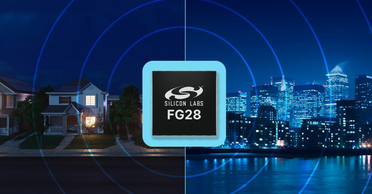
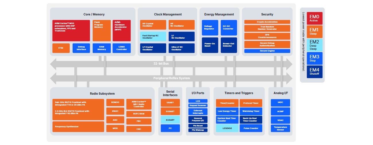
Silicon Labs has introduced its latest innovation, the dual-band FG28 SoC (System on Chip). This advanced SoC offers support for long-range networks and protocols such as Amazon Sidewalk, Wi-SUN, and various proprietary protocols. With this flexible connectivity solution, Silicon Labs continues to build on its wireless connectivity offerings and equip developers to create next-gen Internet of Things (IoT) applications.
The FG28 SoC brings the power of the Amazon Sidewalk to connected devices. Amazon Sidewalk uses a shared wireless network that leverages Sidewalk Bridges, including compatible Amazon Echo and Ring devices, to facilitate communication among devices within the network. With wireless connectivity, IoT devices deployed in outdoor applications using motion sensors and location-based devices can integrate into the network. Amazon Sidewalk achieves this by using Bluetooth Low Energy for short-range communication and utilizing CSS and FSK radio protocols for long distances.
“By including Bluetooth, it gives users an easy way to provision and deploy new devices onto the network, while the sub-GHz band is designed to support device communications over one mile, allowing for new edge applications in areas like smart agriculture, smart cities, and neighborhood networks like Amazon Sidewalk,” says Daniel Cooley, CTO of Silicon Labs.
FG28 SoC allows for the integration of multiple protocols into a single design. As connectivity and computing power continue to extend to the edge, emerging applications require solutions that can cater to diverse connectivity requirements. FG28, with its sub-GHz connectivity leveraging networks like Wi-SUN, is ideal for battery-operated end nodes in smart cities.
Security is a growing concern in the IoT ecosystem, and Silicon Labs addresses this challenge with its Secure Vault technology. Secure Vault is a suite of advanced security features designed to mitigate IoT threats effectively. It is claimed to significantly reduce the risk of security breaches, intellectual property compromise, and revenue loss from counterfeiting.
Interested developers can access the on-demand replay of “Designing Long Range Devices with Amazon Sidewalk.”
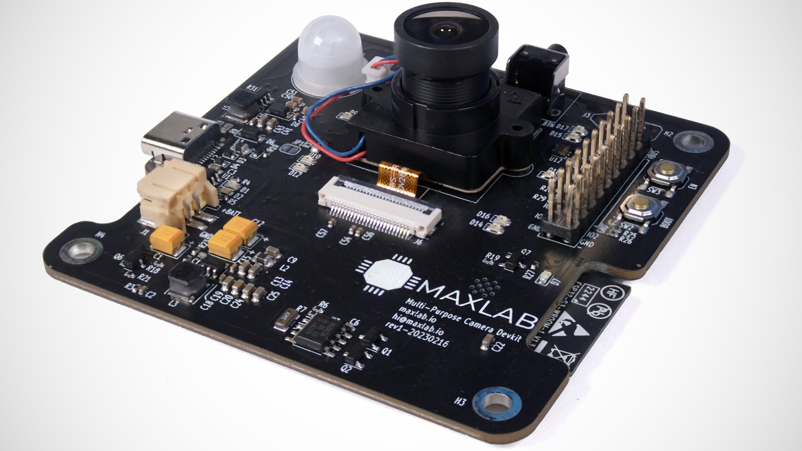
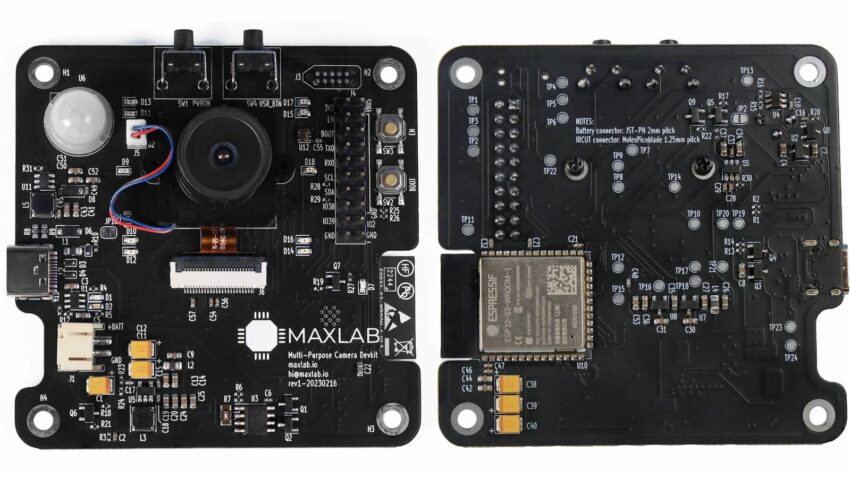
Tokay Lite has taken a crowdfunding platform to attract hackers and embedded developers with its powerful and innovative advanced AI camera. This advanced AI camera platform integrates edge AI processing, enabling real-time image analysis and decision-making right on the device itself. The device was designed to reduce reliance on a separate computer and cloud processing, which resulted in latency issues. With Tokay Lite, the user will have access to a battery-powered, open-source, no-code solution that aims to change the way computer vision applications operate, such as security surveillance and visual data processing.
With a built-in motion sensor and night vision capacity, Tokay Lite can be deployed as a security camera, providing enhanced surveillance capabilities. Its ability to run AI models directly on the device allows for intelligent detection of objects. With its advanced sensor interface and connectivity options, this AI camera can integrate into robotic systems. Tokay Lite can provide real-time visual data to robots, enabling them to perceive and understand their surroundings. The device’s visual recognition capabilities further enhance its usefulness in robotics, allowing robots to identify objects, navigate environments, and even control their actions based on the information provided by Tokay Lite.
At the heart of Tokay Lite is the famous ESP32-S3, a dual-core XTensa LX7 MCU. This advanced microcontroller unit is designed with support for vector instructions, providing acceleration for neural network computing and signal processing tasks. The ESP32-S3 ensures that Tokay Lite can handle complex AI tasks with ease, delivering unparalleled performance in a compact form factor.
Tokay Lite comes with open-source firmware. As soon as you receive the device, you can start exploring its functionalities through a simple, no-code web interface. This out-of-the-box experience allows you to configure settings and make adjustments without the need for any software downloads. With just a few clicks, you can fine-tune image sensor settings, manage video streaming, adjust picture settings, and even activate autonomous operation mode.
Tokay Lite provides generic configurable integrations through HTTP and MQTT, both of which are accessible directly from the embedded web server. This means that you can seamlessly connect Tokay Lite with a wide range of systems and applications, enabling efficient data transfer and communication. Whether you require integration with existing infrastructure or want to build a custom solution, Tokay Lite’s flexible architecture ensures that it can adapt to your specific application needs.
In the first part of this article, we considered the two main stages of a PCM (Pulse Code Modulation) system as the widespread A/D (Analog to Digital Conversion) method and we saw how a continuous signal can be sampled in time and then quantized to limited integer levels in amplitude. The quantum levels are related to a key number of ‘n’ by an exponential relation and the quantized amplitudes grow between minimum level (0) and maximum of (2n -1).
Now we can see the process of producing digital signals from the quantized discrete signal by the third stage of the PCM system.
Binary Encoding Stage
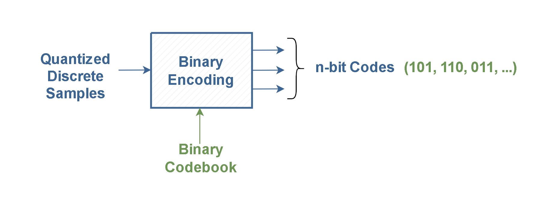
After each sample is quantized, the encoder replaces quantized samples with unique digital code words. Generally, a code word can represent a number, a character, or an analog variable. The most usable code words are binary codes.
Figure 1 shows that each sample can be changed to an n-bit code word in the binary encoding stage. The purpose of this encoder is to assign a unique binary code to each discrete sample at the input. Hence, it encodes the quantized data from 2n possible states into an n-bit code. The binary codebook performs like a mapping table to relate input data to output codes. It defines each discrete value at the input is converted to what code at the output of this stage.
Figure 1: The function of binary encoding
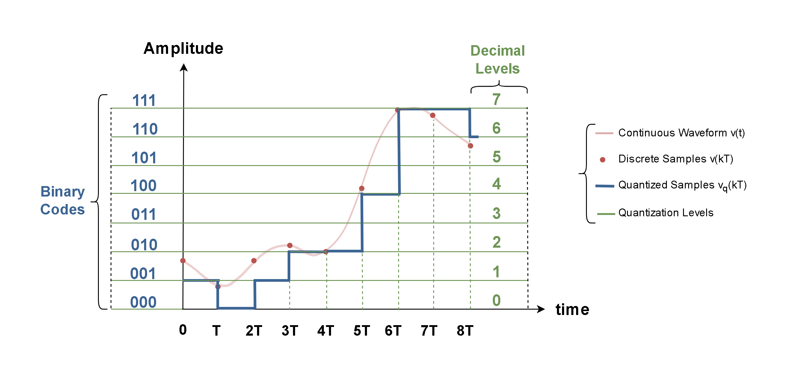
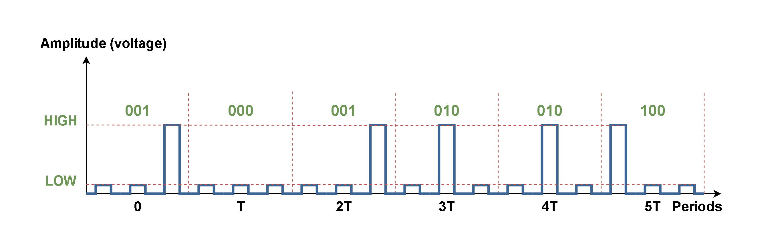
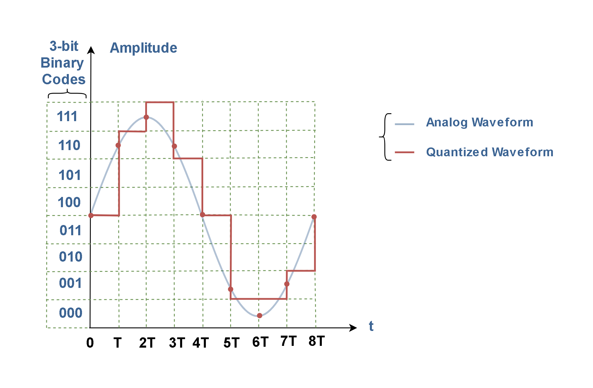
Figure2 shows the results of A/D conversion on the analog signal v(t) in our previous example waveform after applying of the binary encoding stage.
Figure 2: The results of the binary encoding stage
Figure 2 describes how the continuous waveform v(t) is sampled and changed to v(kT) samples at first and then, these discrete samples are quantized to 8 equal levels and changed to vq(t) waveform; whereas each quantization level has been assigned to an integer decimal number.
Clearly, humans use the decimal number system that represents quantities with digits 0 through 9. However, digital systems process binary data internally, like computers.
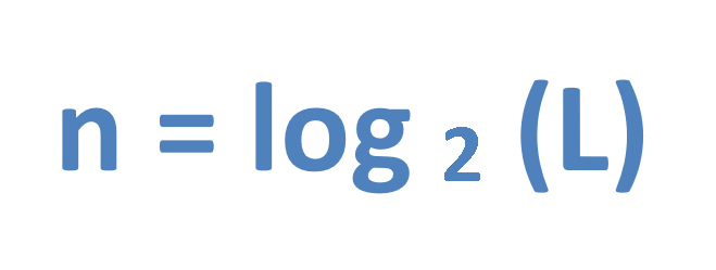
Note that the number of bits for each sample (n) is determined from the number of quantization levels (L). The number of bits can be calculated by Equation1.
Equation 1: Calculation of the word length
In our example, because of L = 8 then, the binary word length is n = log 2 8 = 3. For this reason, our results at the output are arranged between the minimum level of amplitude (decimal 0 or binary 000) and the maximum level (decimal 7 or binary 111).
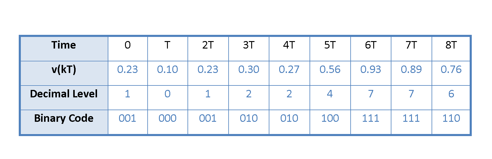
We can also collect all the input and output data in Table 1 to find out a better understanding of the conversion. The input signal contains some fractional values for each interval and the output contains some 3-bit code words for the same periods.
Table 1: Output results of the A/D conversion in the example
In Figure 2, the waveform of quantized samples (the blue graph) can be assumed as the stairstepapproximation of the original analog waveform (the red one).
Binary Codes
Mostly, the code words are in the form of base-2, or binary numbers. It means they are constructed by strings of 1’s and 0’s. The symbols 0 and 1 are called binary digits or bits.
Binary codes are most familiar in representing integers. The reason for using binary numbers in digital equipment is the ease with which they can be implemented. It means the electronic components and circuits must be capable of assuming two discrete states to represent 0 and 1.
A typical digital code word would be like this array:
b7 b6 b5 b4 b3 b2 b1 b0 = 1 0 1 1 1 0 0 1
It is composed of eight bits. The subscripts correspond to the position of a particular bit in the sequence. The ‘1’ at the extreme left (b7 in the example) is called the ‘most significant bit’ or MSB, and the ‘1’ at the right (b0 in the example) is called the ‘least significant bit’ or LSB.
The straight or natural binary is the simplest way of representing quantities with binary numbers. In this case, the subscripts correspond to a power of 2 associated with the weight of each bit in the string. In the natural binary strings, the values related to serial bits are in a sequence of this form:
[2n-1 ,2n−2 ,2n-3, … ,22 ,21 ,20]
It means the position of a bit in the sequence defines its weight. Then, in a natural binary integer code having n bits, the LSB has the minimum weight of 20 (= 1) and the next bit has a weight of 21 (= 2), and so on up to the MSB, which has the maximum weight of 2n–1.
The decimal (base 10) value of a binary number is obtained by adding up the weights of all non-zero bits. When these weighted bits are added up, they form a unique number having any value from 0 to 2n -1.
Therefore, the number of bits in a binary word determines the maximum decimal value that can be represented by that word. This maximum value is determined with Equation 2:
Equation 2: The maximum decimal value of an n-bit word
where M is the maximum decimal value and n is the number of bits in the word.
Thus, the largest decimal number that can be represented by our previous example is 23 – 1 = 7.
Digital Waveforms
Unlike an analog signal which varies continuously, a digital signal has defined discrete levels or states. The signal switches or changes suddenly from one state to the other. Digital signals with two discrete levels of voltage are also referred to as binary signals.
In Pulse Code Modulation, the binary data are represented by a sequence of bits. In a simple representation, a binary waveform can be made up of a series of pulses. When the level of the waveform is HIGH, a binary 1 is present and when the waveform is LOW, a binary 0 is present.
The symbol ‘1’ is usually represented by a positive voltage between 1 and 12 volts and the symbol ‘0’ is mostly represented by a zero voltage or some values close to it (for example +0.1 volt). In this manner, a conducting transistor may represent a ‘1’, whereas a cut-off transistor may represent a ‘0’.
Figure 3 shows the results of Table 1 as a digital waveform of outputted binary codes. In this figure, just the results of 6 periods (from 0 to 5T) are plotted.
Figure 3: The waveform of binary codes
The Length Of Binary Words
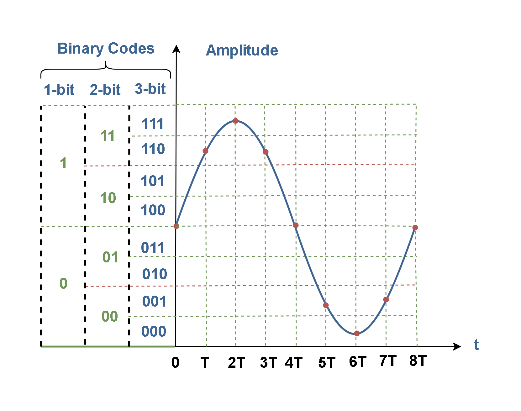
Let’s consider an analog signal at the input of A/D converter. Here we can digitize the signal in three ways, as shown in Figure 4.
Figure 4: Digitizing a sinusoidal signal with 3 options
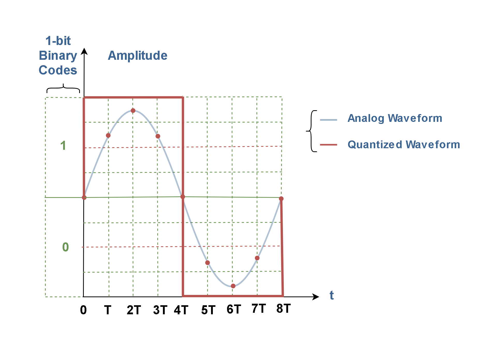
In the first case, we choose the step size so large that the output has only two states and we express the values with only one bit, i.e., just zero or one value! What is obvious is that in this case (n=1 and L=2) the accuracy is very low and this type of processing does not give us any correct information about the signal status.
As Figure 5 shows, the similarity between the analog signal (the blue curve) with the quantized signal (the red square wave shape) is very low and most of the details are missing because of coarse approximation. This case is completely inefficient and may not have any practical advantages.
Figure 5: Digitizing the sinusoidal signal by the 1-bit word length (the first option)
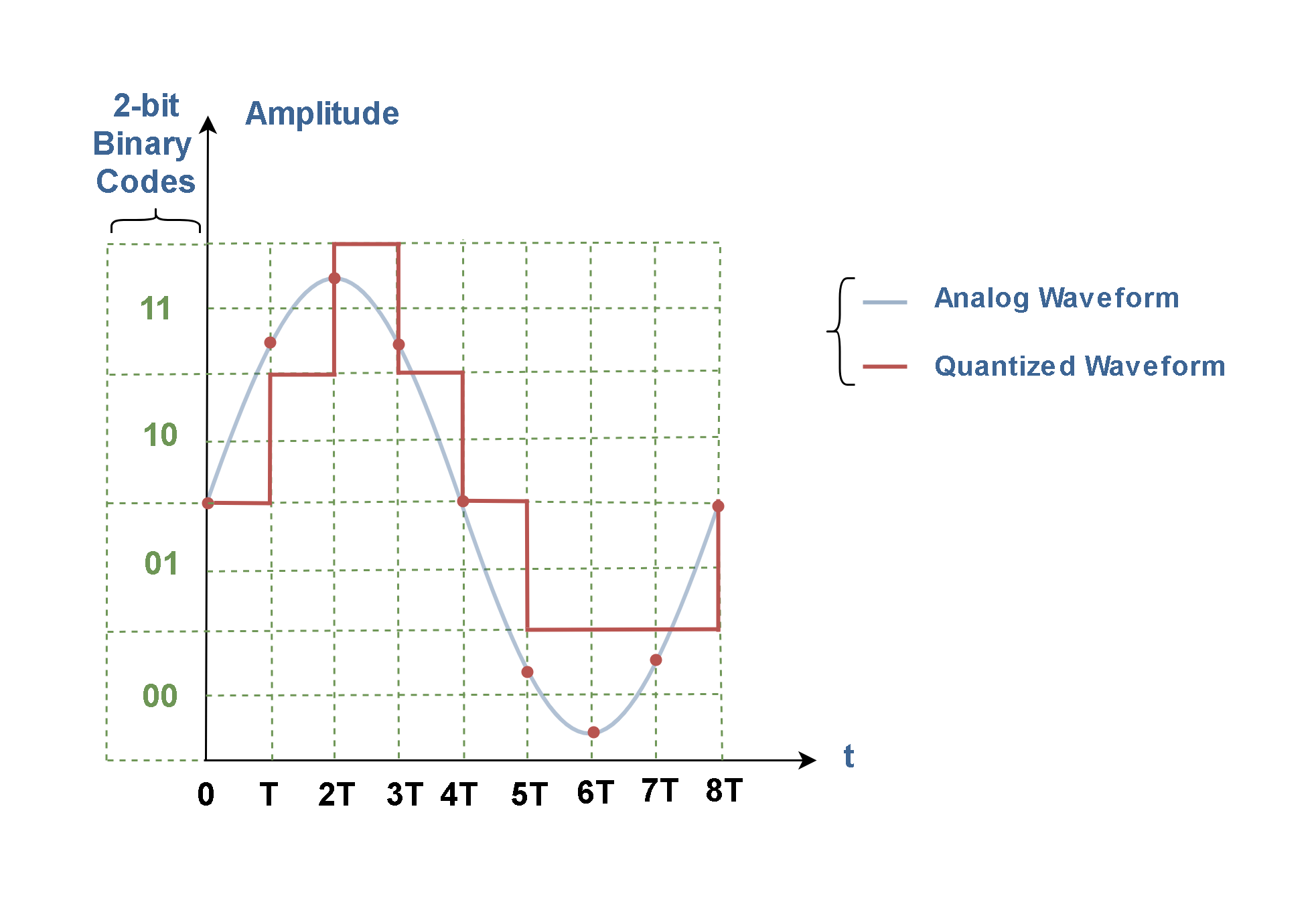
In the second case, we set parameters n=2 and L=4. It is clear that in this case, if we reduce the size of the steps and make the divisions smaller, we can have 4 numerical values in the output and express the values with 2 bits (from value 00 to 11).
As Figure 6 shows the similarity between the analog signal with the quantized signal is still low and some of the details are missing. This case is also impractical.
Figure 6: Digitizing the sinusoidal signal by the 2-bit word length (the second option)
In the third case, the divisions are made smaller again and we reach 8 states in the output in which we can express the values with 3 binary bits (from 000 to 111). Here, because we have used more output bits, the accuracy has slightly increased and there is less error. As Figure 7 shows the similarity between the analog waveform and the digital signal has been corrected slightly.
It is obvious if the quantization step size (q) is smaller, the quantization error will be smaller too. In other words, for better accuracy and fewer errors, we need to increase the number of bits in the configuration of A/D conversion systems.
Figure 7: Digitizing the sinusoidal signal by the 3-bit word length (the third option)
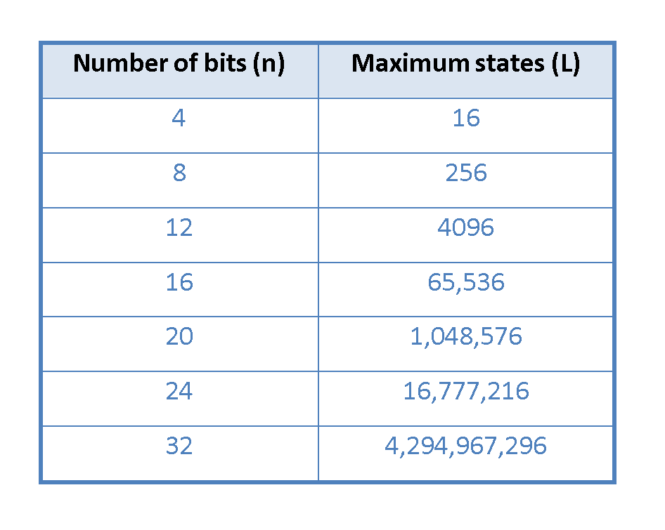
Essentially, most of the digital systems work with a fixed-length binary word. Word lengths of 4, 8, 12, 16, 20, 24, and 32 bits are common in digital systems.
Table 2 describes the most usable number of bits in different applications and the maximum number of available states which they offer for quantization.
Table 2: Number of bits in binary codes and number of quantization levels
Here are some examples:
A common binary word length in microcomputers, data storage, processing, and transmission equipment is 8 bits.
Consumer digital video applications also use 8-bit words.
Digital commercial audio applications use 16-bit words.
Compact discs (CDs) also use 16 bits to store digital information.
A single high-quality PCM audio channel usually requires 20-bit word lengths.
Conclusion
Theoretically, the analog-to-digital conversion will never be 100% accurate, and a finite amount of information will be lost forever during the quantization and round-off process. Naturally, the presence of this ‘approximation’ causes some error in the output. It means when the digital representation is converted back to analog, the result will not be identical to the original waveform.
In practical terms, by decreasing the quantization step size, it is possible to reduce the error to such small values that it may be ignored in many applications. The sequence length (n) can be chosen to suit the specific needs of the application.
Summary
A/D converters represent sequences of bits.
Binary means two—two states or two discrete levels.
Because the base of the binary number system is 2, only two symbols (0 and 1) are used to represent any quantity.
The best-known code (other than base 10) is natural or straight binary (base 2).
Digital equipment processes binary words.
Digital waveforms consist of voltage levels that are changing back and forth between the HIGH and LOW levels or states.
The A/D operation is never completely free of the error caused by approximation which is the natural effect of quantization.
The more the number of quantization divisions and the smaller the distance between the numbers, the better the approximation will be.
The Binary Subtractor is a combinational logic circuit that performs an arithmetic operation of subtraction on binary numbers. The output of a Binary Subtractor is the difference (X – Y) resulting from subtracting the two binary inputs (X & Y). It is one of the important arithmetic combinational logic circuits just like Binary Adder, discussed in the previous article.
As the Binary Addition results in two outputs i.e. Sum (S) & Carry (C), likewise, a Binary Subtraction also results in two outputs but, are termed Difference (D) & Borrow (B). In the Addition operation, the Carry (C) indicates an addition exceeding the maximum allowed value/ number depending on the number system. For example, in Denary it is nine (9) whereas it is one (1) in the case of the Binary number system. However, in Subtraction, a Borrow (B) indicates when the subtrahend (to be subtracted number) is greater than the minuend (number from which another number is subtracted). In this case, a borrow is taken by that number of the minuend from the next column (next significant) to output a difference which is then returned back.
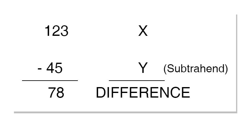
An arithmetic operation of subtraction between two numbers is represented by a minus (-) symbol placed on the rightmost side of the subtrahend. In the following denary subtraction, a borrowing concept has been explained.
Figure 1: Denary subtraction example
It is known that units are subtracted from units, tens from tens, hundreds from hundreds, and so on, just like the way, an addition is carried out. In this subtraction, units (first column) cannot be subtracted directly as five (5) is greater than three (3), and a borrow from minuend’s tens (next column) is taken by the unit to carry out the subtraction. This results in a difference of 8 (13 – 5) and a value of 1 after taking borrow from 2 in tens (next column). Afterward, tens of both numbers are subtracted, accordingly, and so for hundreds.
Binary Subtraction
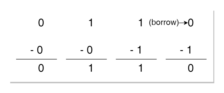
The subtraction of Binary numbers follows the same procedure described above for Denary numbers. A Binary number is a Base-2 number and, as such, a Binary Digit (bit) can have only two (2) values. So, a bit of a binary number can have only two distinct values i.e. 0 or 1. As such, in Binary, the maximum allowed value for a digit is one (1). A subtraction of single Binary Digits (Bits) results in 0 – 0 = 0, 1 – 0 = 1, 1 – 1 = 0, and, 0 – 1 = 1 which requires a borrow. A borrow taken by 0 results in 10 (2 in Denary). The subtraction of single bits is explained below.
Figure 2: Bit subtraction combinations
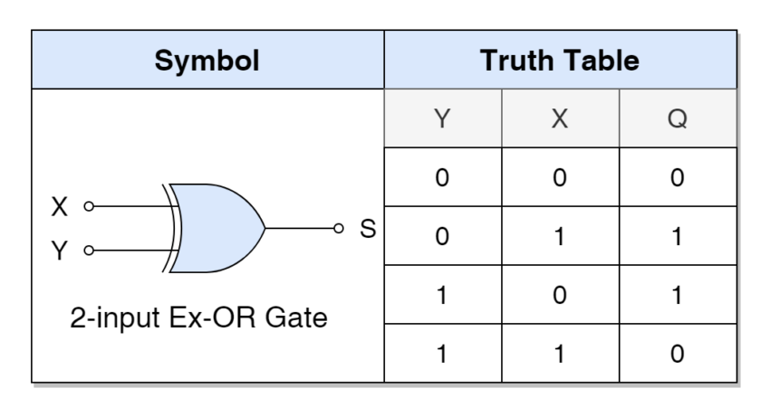
It is obvious from the above subtraction results of single binary digits that their combination resembles the truth table of an Exclusive-OR (XOR) gate when the borrow bit is ignored. A truth table of the 2-input Exclusive-OR (XOR) gate is illustrated below.
Figure 3: Exclusive-OR (XOR) Gate Symbol and Truth Table
In Binary Adder, an Exclusive-OR (XOR) gate is used to produce Sum (S), and Carry (C) is needed when both digits are equal to 1. The generation of the Carry (C) bit was carried out using an AND gate. However, in Binary Subtraction, a Borrow (B) bit is to be generated when minuend & subtrahend are equal to 0 & 1, respectively. Looking at the required truth table or Borrow (B) depending on input combinations, this can be easily accomplished by ANDing the subtrahend and inverted-minuend. The logic circuit required for the generation of the Borrow (B) bit, is shown in the following figure.
Figure 4: Borrow (B) bit logic circuit
Half Binary Subtractor
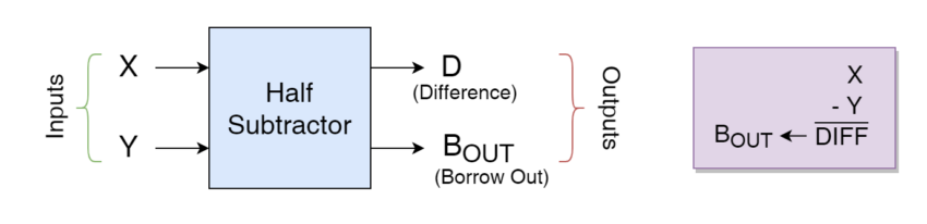
A Half Binary Subtractor is a combinational logic circuit that performs subtraction on two single binary digits (bits) producing Difference (D) and Borrow (B) bits. A Half Binary Subtractor can be constructed by combining an Exclusive-OR (XOR) gate and borrow bit generation described above. A general block diagram of the Half Subtractor is given below:
Figure 5: Half Subtractor block diagram
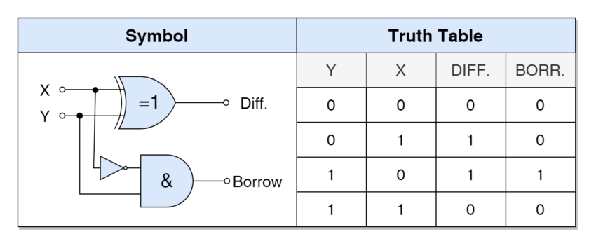
The resulting Truth Table of this Half Binary Subtractor along with the logic circuit is also illustrated below.
Figure 6: Half Subtractor Circuit and Truth Table
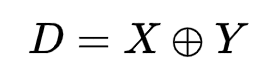
It is obvious from the Truth Table and logic circuit that Difference (D) is the result of the Exclusive-OR (XOR) gate. Whereas, the Borrow (B) is the result of NOT-AND combinational logic. The Boolean Expressions for these outputs are:
Difference (D) bit:
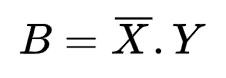
Borrow (B) bit:
The above expression of Difference (D) bit is exactly similar to the Sum (S) expression of a Half Binary Adder as both expressions result from the usage of an Exclusive-OR (XOR) gate. The expression of the Borrow (B) bit is also very similar to the Carry (C) expression of Half Adder and the minor difference is due to the inversion of the minuend. This is the only difference between a Half Adder and a Half Subtractor and a Half Subtractor can be created from a Half Adder by inverting the minuend.
The Half Subtractor has one of the main disadvantages of not taking a Borrow (as an input) from the previous (less significant) Half Subtractor. A “Borrow-in” is essentially required for subtracting numbers with more than one digit. A Half Subtractor having provision of Borrow-in from previous subtraction is called a “Full Binary Subtractor”.
Full Binary Subtractor
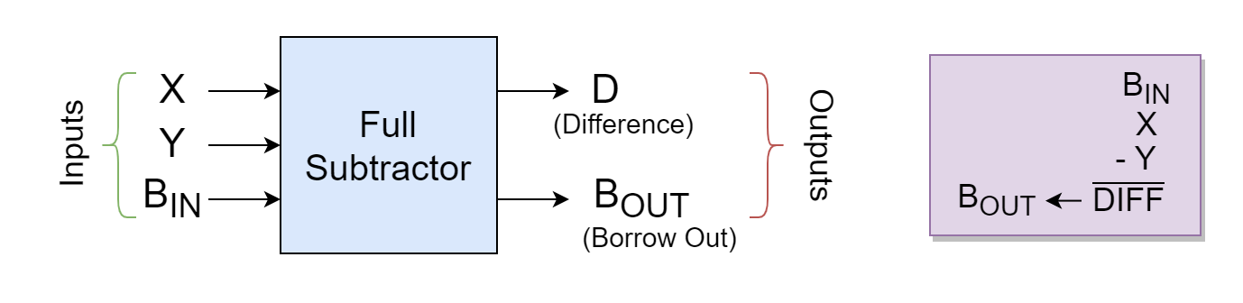
A Full Binary Subtractor has an additional input of “Borrow-in”, as compared to Half Binary Subtractor, for taking into account “Borrow-out” from the previous Half Subtractor. A block diagram of a Full Binary Subtractor has been shown in the following figure.
Figure 7: Full Subtractor Block Diagram
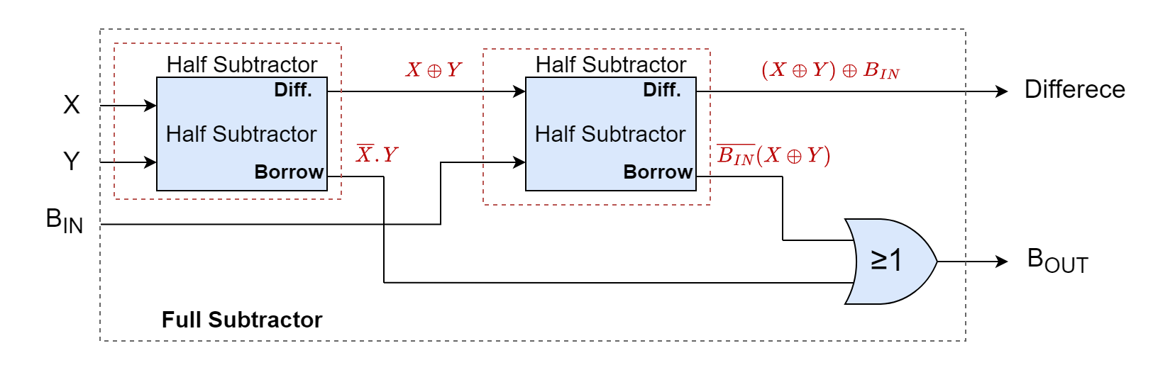
The Full Binary Subtractor performs subtraction on three inputs (X, Y, & BIN) and produces outputs (D, & BOUT). The process of subtraction is carried out in two steps by Half Binary Subtractors which are cascaded together so that the first Half Subtractor (BOUT) passes its “Borrow” to the second Half Subtractor (BIN). This cascading of Half Subtractors is illustrated below.
Figure 8: A Full Subtractor using two Half Subtractors
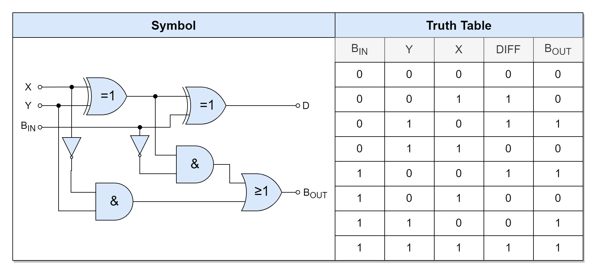
The Full Binary Subtractor comprises two Half Binary Subtractors which are cascaded and the Borrow Out (BOUT) is generated by using the OR gate on individual Borrow of each of the Half Binary Subtractors. As a Full Binary Subtractor has three inputs so its Truth Table has a total of eight (8) input combinations. The Truth Table of the Full Binary Subtractor has been given below.
Figure 9: Full Subtractor Circuit with Truth Table
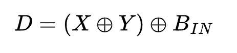
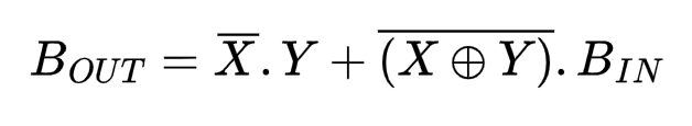
Expressions for outputs of a Full Binary Subtractor are as follows:
Difference (D) bit:
Borrow Out (BOUT):
n-Bit Binary Subtractor
Using a Full Binary Subtractor, a Binary Subtractor of larger binary numbers can be constructed by following the same method of cascading Full Binary Adders. The Borrow-out (BOUT) of the first Full Binary Subtractor is connected with the Borrow-in (BIN) of the next Full Binary Subtractor and the process is repeated for the required number of bits to be subtracted. Using this cascading, an n-bit Binary Subtractor can be constructed which has an inverted input compared to n-bit Binary Adder.
Binary Subtractor based on 2’s Complement
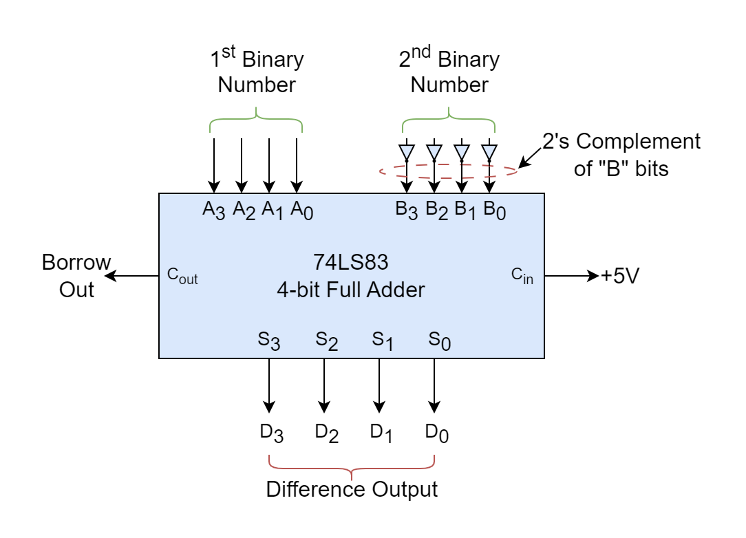
As explained above, using an n-bit Full Adder and “n” number of NOT gates, the process of addition becomes subtraction by using two’s (2’s) complement notation on subtrahend bits and Carry-in (CIN) pulled “HIGH” as shown in the following figure.
Figure 10: A 4-bit 74LS83 Adder as a Subtractor using 2’s complement
In this way, commercially available 4-bit Full-Adder ICs such as CD4008 (CMOS) and 74LS283 (TTL) can be utilized to perform 4-bit subtraction. Using a two’s complement (-Y) and then adding in X equals X + (-Y) which is equivalent to X – Y. In order to revert to the original Addition function, Carry-in (CIN) is set to “LOW”, simply, and setting of CIN to “HIGH” or “LOW” shifts the function between addition or subtraction.
Conclusion
A Binary Subtractor is a combinational logic circuit that performs the arithmetic operation of subtraction on binary numbers.
A Binary Subtractor produces two outputs of Difference (D) and Borrow (B). The Borrow (W) is generated when a subtrahend is greater than minuend.
A simple single-bit Subtractor can be constructed using an Exclusive-OR (XOR), AND & NOT gates. In this construction, Exclusive-OR (XOR) gate produces Difference (D) and NOT-AND generates Borrow (B). This construction is termed a Half Binary Subtractor.
A Full Binary Subtractor is constructed by cascading two Half Binary Subtractors. A Full Binary Subtractor can take in Borrow-in (BIN) from a previous Full Binary Subtractor’s Borrow-out (BOUT). This enables Full Binary Subtractors to be cascaded with each other.
Subtraction of larger binary numbers (n-bit) can be accomplished by cascading the required number of Full Subtractors.
A Full Binary Adder can be converted into a Full Binary Subtractor by inverting one of the inputs. As such, commercially available 4-bit Full-Adders (CD4008 &74LS283) can be used for subtractions purpose using two’s complement of the subtrahend and setting Carry-in (CIN) to “HIGH”. Setting Carry-in (CIN) to “LOW” resumes the addition function.