Rugged COM Express CPU Module with Intel Atom x6000 Processors

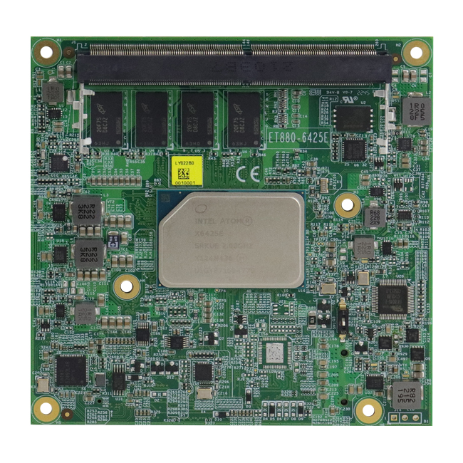
IBASE Technology Inc., a leading provider of industrial motherboards and embedded computing solutions, has announced the release of its latest ET880 COM Express CPU module designed to meet the demands of embedded applications that require low power consumption and fanless operation. The module integrated Intel Atom x6000 series processors that are built on 10nm technology support clock speeds of up to 3.2 GHz and Intel’s Time Coordinated Computing (TCC) technology, which enables precise clock synchronization across multiple devices.

The ET880 delivers robust performance and reliability, with features that make it an ideal choice for a variety of industrial and IoT applications. The module boasts onboard 8GB DDR4 memory and a DDR4 SO-DIMM slot for a total RAM capacity of 24GB to ensure efficient system operation. It is equipped with a range of connectivity options, such as a I226IT PCI-E 2.5G LAN controller, two USB 3.1, four USB 2.0, two SATA III, two UART (Tx/Rx only), and three independent displays via the DisplayPort / DVI-D / LVDS or eDP interfaces on the IBASE IP419 carrier board.

The ET880 is compatible with Windows 10 and Linux operating systems, and manufactured to meet the stringent requirements of industrial applications, with an extended temperature range of -40°C ~ +85°C, and long-term availability.

ET880 FEATURES:

  • Onboard Intel® Atom® x6000 series processors
  • Onboard 8GB DDR4 memory + 1x DDR4 SO-DIMM, IBECC compatible
  • 1x I226IT PCI-E 2.5G LAN
  • 2x USB 3.1, 4x USB 2.0, 2x SATA III, 2x UART (Tx/Rx only)
  • Supports 3x independent displays, DisplayPort /DVI-D / LVDS or eDP via carrier board (IP419)
  • Supports wide-range operating temperature of -40°C ~ +85°C

The ET880 is available now from IBASE. For more information, please visit www.ibase.com.tw

PICO-ITX board with Elkhard Lake processor

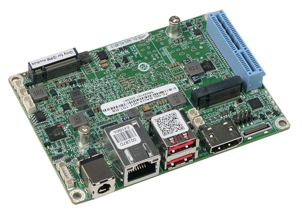
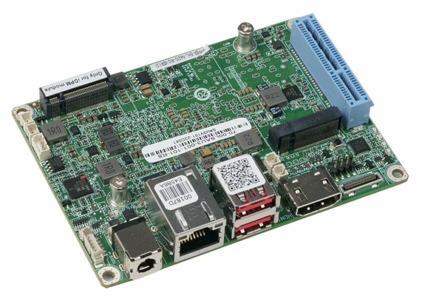
The high-performance Hyper-EHL board from ICP Germany is a cost-effective solution for applications requiring high reliability, such as industrial automation, machine control, traffic engineering and display systems.

The Hyper-EHL board can be purchased with two different Elkhard Lake CPUs: Variant one with Intel® Celeron J6412 offers four processor cores, a base clock frequency of 2.00 GHz, 1.5 MB cache and an Intel® processor graphics unit with 400 MHz, while variant two with Intel® Celeron N6210 brings two processor cores, 1.20 GHz base clock frequency, 1.50 MB cache an Intel® processor graphics unit with 250 MHz. An LPDDR4 working memory with 4GB is soldered onto the board. Optionally 8GB are possible from 100 pieces. An iSATA slot and an M.2 slot with M Key are available for mass storage.

Specifications

  • Pico-ITX board with Intel® Celeron J6412 or N6210 CPU
  • LPDDR4 4GB memory (optional 8GB)
  • Three independent displays: HDMI, Display Port and optional IDPM
  • 2.5 GbE Intel® I225V
  • Two USB 3.2, two USB 2.0, one iSATA, one COM interface
  • Extensions: one M.2 M slot, one PCIe x4 slot

The Hyper-EHL has numerous connectors, including HDMI, Display Port, optional iDPM, a 2.5 GbE Intel® I225V LAN interface, two USB 3.0, two internal USB 2.0 and an internal RS232/422/485 interface. With a voltage input of 12V DC, the wafer EHL can be used in environments from 0°C to 60°C.

ICP Germany supplies the Hyper-EHL with appropriate memory and CPU on request.

iWave Unveils STM32MP13x Solderable System on Module in OSM Size-0 Form Factor

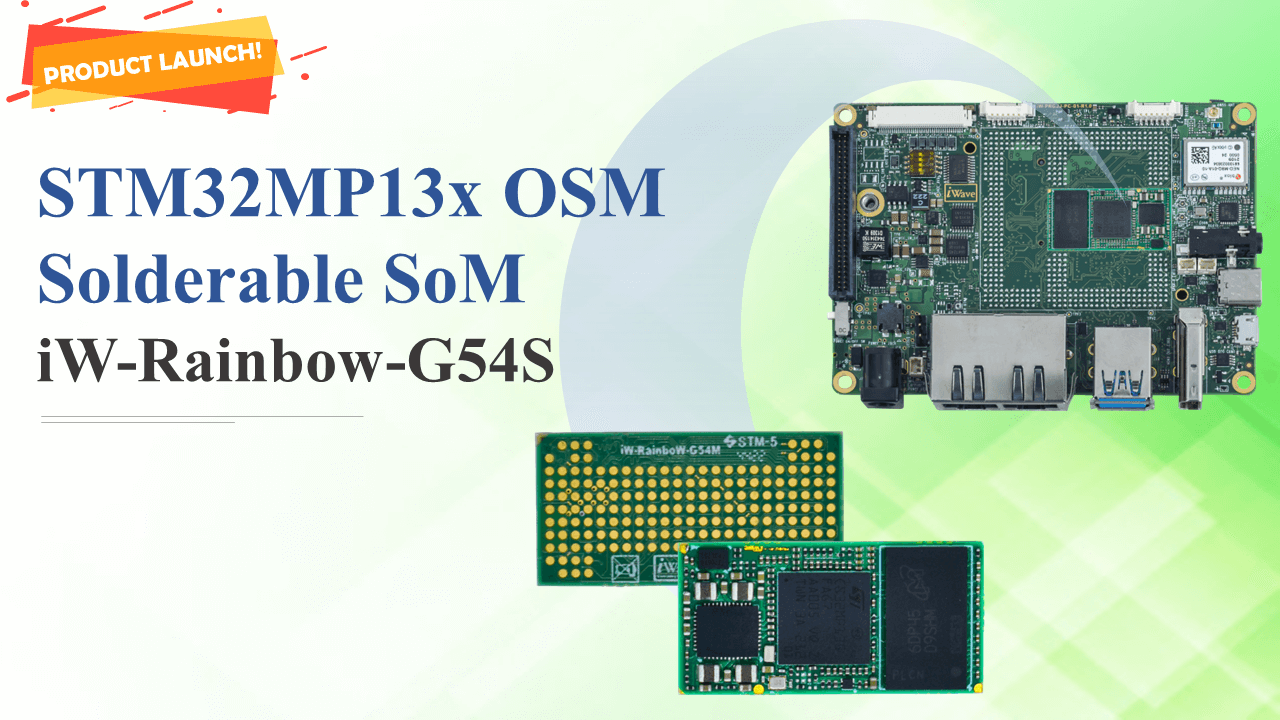
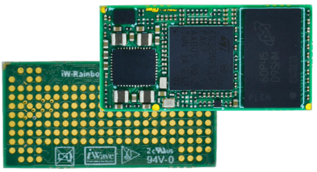
In line with the new industry standard, Open Standard Module or OSM, defined by SGET, iWave announces the release of the iW-RainboW-G54S: STM32MP13x LGA System on Module (SoM). The SoM incorporates STM32MP13x MPU from STMicroelectronics and is built on OSM Size-0 standard, providing high performance, power efficiency, and a rich set of interfaces to meet versatile market needs.

High-end wearables and other low-powered embedded & consumer applications benefit from the new STM32MP13x MPUs featuring the ARM Cortex-A7 application processors running at 1GHz. Cortex-A7 has all the features of the high-performance Cortex-A15 and Cortex-A17 processors, including physical virtualization, NEON, and 128-bit AMBA 4 AXI bus interfaces.

Key features of STM32MP13x OSM System on Module

  • STM32MP13x MPU with Arm Cortex-A7
  • Up to 1GB DDR3L, 16Mb QSPI NOR Flash
  • 1 x RGMII, 1 x USB 2.0 OTG, 1 x USB 2.0 Host
  • 2 x SDMMC, 2 x ADC
  • 4 x UART, 1 x Console UART, 2 x SPI, 2 x I2S, 2 x I2C
  • 16 x OSM GPIOs
  • Size-0 Form Factor: 30 mm x 15 mm
  • Solderable LGA Package in OSM v1.1 Standard
  • 188 Contacts

The STM32MP13x System on Module is built on a 30 mm x 15 mm OSM Size-0 standard, the smallest size in the OSM variants making it an ideal choice for building portable consumer products. The 188 LGA contacts available on its back for mating with the carrier board make the platform resistant to shock and vibrations, ensuring high levels of robustness.

iWave brings design compactness while enabling modularity and scalability to ST customers. To fulfill the ever-increasing need for rapid data transfer, the SoM supports dual USB 2.0 interfaces and Gigabit Ethernet delivering a robust, high-performance, consistent, high-quality user experience.

Key features of STM32MP13x Single Board Computer

  • STM32MP13x MPU with Arm Cortex-A7
  • Up to 1GB DDR3L, 16Mb QSPI NOR Flash, 16Mb SPI NOR Flash
  • Micro SD, M.2 connector Key B (USB, Nano SIM connector)
  • Gigabit Ethernet (RGMII), USB 2.0 OTG, USB 2.0 Host
  • RS232, CAN x1, GNSS receiver, RTC Battery
  • 3.5mm Audio IN/OUT Jack, Speaker Header
  • Expansion: CAN x1, SDMMC 8bit, SPIx1, PWM x1, ADC x2, UART x2
  • DC 12V Input, -40°C to +85°C Industrial Grade
  • 100 mm x 72 mm (Pico ITX Form Factor)
  • Linux 5.15.67

The System on Module forms the building block for products and solutions that require a rich set of interfaces with high performance and efficiency. The SoM enables customers to shorten their time to market with reduced risk and complexity.

“STM32MP13x MPU incorporating Cortex-A7 offers power and performance balance for a variety of devices with varying requirements,” said Ahmed Shameem, Hardware Project Manager at iWave Systems. “The STM32MP13x Solderable System on Module leverages the processor features to provide rich performance for diverse low-power embedded applications that ST customers require.”

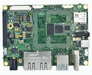
STM32MP13x OSM SoM is mounted on a carrier board as a Single Board Computer (SBC), which can also be used as an evaluation kit. This feature-rich multimedia insert-ready SBC is available in Pico-ITX form factor, ready to be integrated across diverse machine learning applications.

The System on Module and Single Board Computer are go-to-market and production ready complete with documentation, software drivers, and a board support package. iWave maintains a product longevity program that ensures that modules availability for long periods of time (10+ years).

More information on STM32MP13x OSM System on Module can be found here.

iWave Launches its Most Scalable & Adaptive AMD Versal AI Edge-Based SOM Series

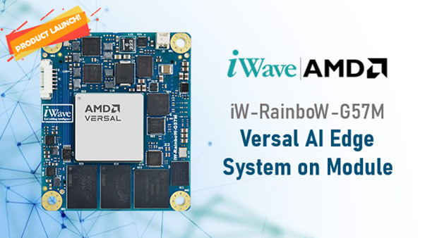
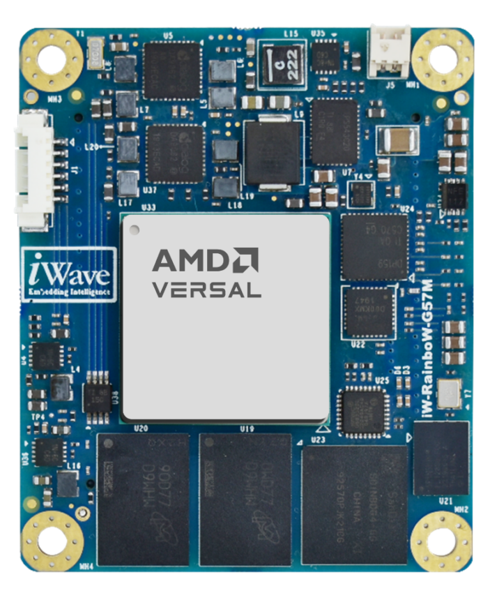
iWave introduces iW-Rainbow-G57M: a new System on Module (SOM) based on the AMD series, designed to power AI applications from the edge to the endpoint. The new SOM features the Versal AI Edge series to deliver leading AI performance/watt in the industry and provide the AI acceleration required for many applications ranging from ADAS and robotics to medical imaging.

iW-Rainbow-G57M: The Versal AI Edge-based System on Module is compatible with an extensive series of chips: VE2302/VE2202/VE2102/VE2002. The System on the Module is integrated with 8GB LPDDR4 RAM and 128 GB EMMC and 256MB QSPI Flash. Two high-speed expansion connectors and 122 User Configurable IOs provided on the System on Module enable a multitude of interfaces available for the user.

The Versal SOM supports a breadth of connectivity options, such as 28.21Gbps high-speed transceiver blocks to support all necessary protocols in edge applications, 40G multi-rate Ethernet, PCIe, and native MIPI support for vision sensors which are a must for advanced AI applications.

The Versal AI Edge provides the capability to run larger models and faster inference engines on the Edge. The Versal AI Edge combines scalar engines (Arm Cortex A72 Cores applications processor and Arm Cortex R5 core for real-time processing and control) enabling computing for complex algorithms while enabling high levels of safety and security. With the System on Module, customers can build their Edge AI Solution with reduced development cost, risk, and time. The System on Module also provides customers with the flexibility and scalability features of the Versal Edge AI series.

Highlights of the iW-Rainbow-G57M SOM:

  • Pin Compatible Devices: VE2302/VE2202/VE2102/VE2002
    • Dual-core Cortex-A72 Core and Dual-core Cortex-R5F Core
    • Up to 328K Logic cells & 150K LUTs
    • Up to 45 TOPA(INT4) AI compute
    • Programmable Network on Chip (NoC)
  • Up to 8GB LPDDR4, up to 128GB eMMC, 256MB QSPI
  • 8 GTYP Transceiver support (VE2302 & VE2202).
  • GTYP support: PCIe Gen4 or 40G Multi-rate Ethernet MAC
  • 2 x 240-pin High-Speed Connectors.
    • 1x GbE, 1X RGMII, 1 x USB, 1 x CAN FD,
    • 1 x PMC, I2C, 1x SD, 1x UART, 1x JTAG
    • FPGA XPIO: 51 LVDS/102 SE
    • FPGA HDIO: 20 SE
  • Form Factor: 50 mm x 60 mm
  • Industrial-grade SOM
  • Product Longevity of 10-15 years

“iW-Rainbow-G57M is built to leverage the most scalable and adaptive portfolio of Versal AI Edge, enabling edge-to-endpoint with high performance per watt and low latency,” says Mr. Abdullah Khan M, Director-Engineering at iWave Systems. “The System on Module is an ideal fit for applications such as lidar, radar, and robotics. Surveillance, medical imaging, and reduce product development time with reduced risk and complexity.”

Developers can get started using the Versal AI Edge evaluation kit. iWave supports development tools for hardware and software development such as the Vivado design tool, Vitis unified software, frameworks, and accelerated libraries for target applications. iWave also provides custom design and manufacturing services around the SOM, presenting a comprehensive ecosystem for the customer on their product development.

“Versal AI Edge brings high-performance AI inference to embedded systems while retaining the hallmarks of adaptive computing in industrial—long lifecycles, extended temperature support, real-time and deterministic performance, and the ability to aggregate all aspects of the applications beyond AI inference,” Chetan Khona, senior director, Industrial, Vision, Healthcare & Sciences Markets at AMD. “iWave has done an excellent job of offering this solution to the market in an easy-to-integrate system on module.”

iWave Systems is a global leader in the design and manufacturing of FPGA System on Modules and ODM Design Services. With over 23 years of diverse experience in the FPGA domain and a strong design-to-deployment competence, iWave strives to transform your ideas into time-to-market products with reliability, cost, and performance balance.

More information about the Versal AI Edge can be found here.

8 Channel RF Remote Receiver with Holtek and Serial Protocol

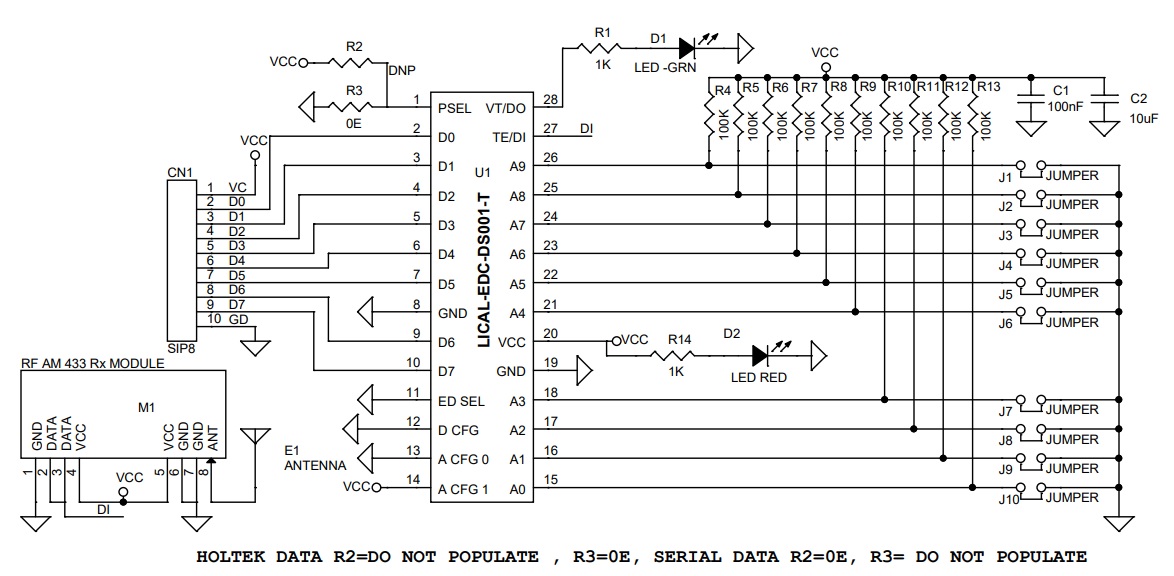
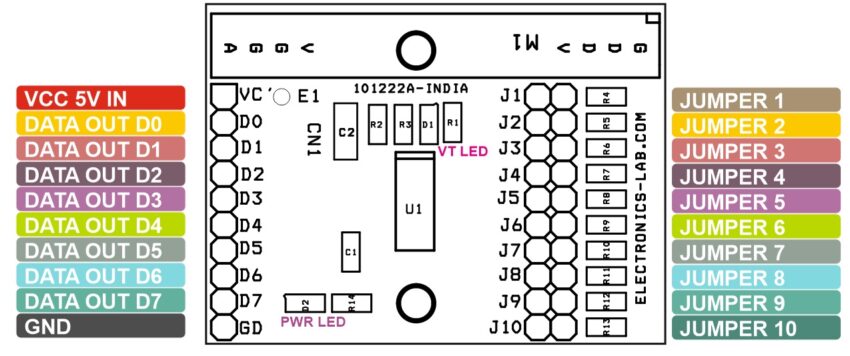
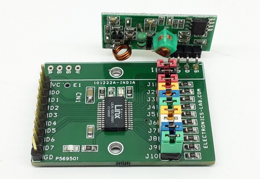
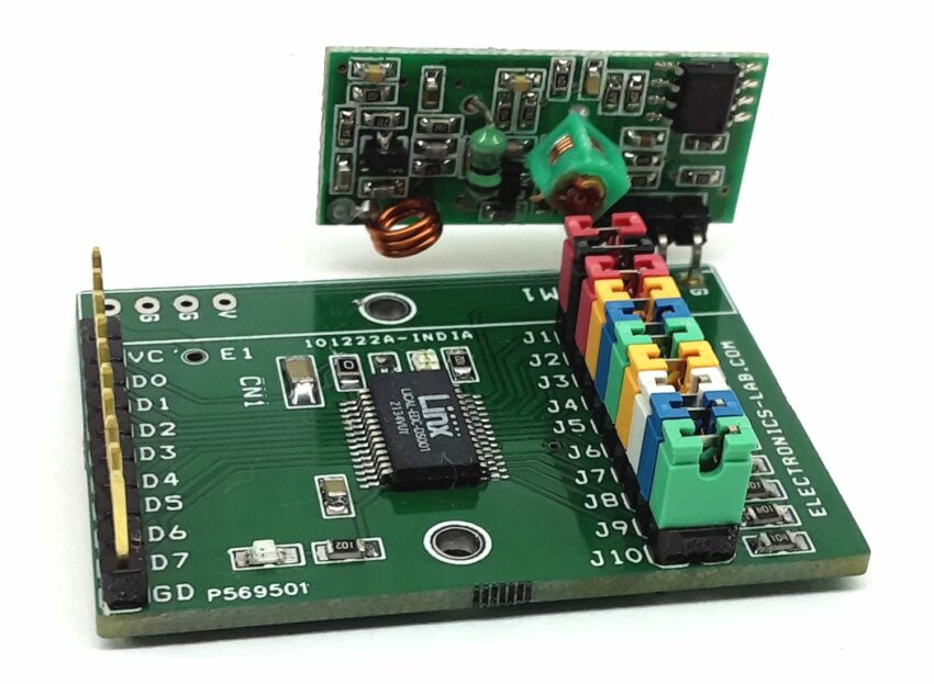
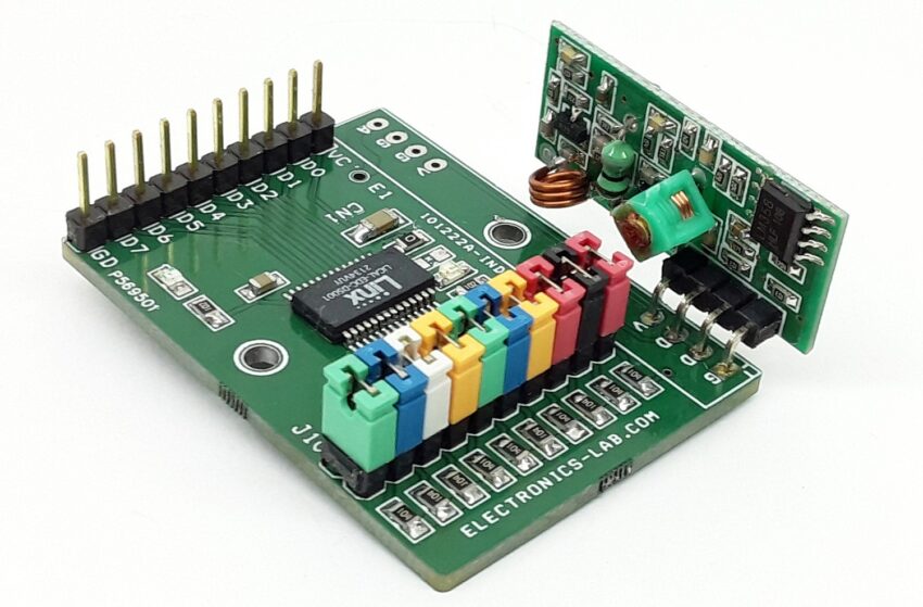
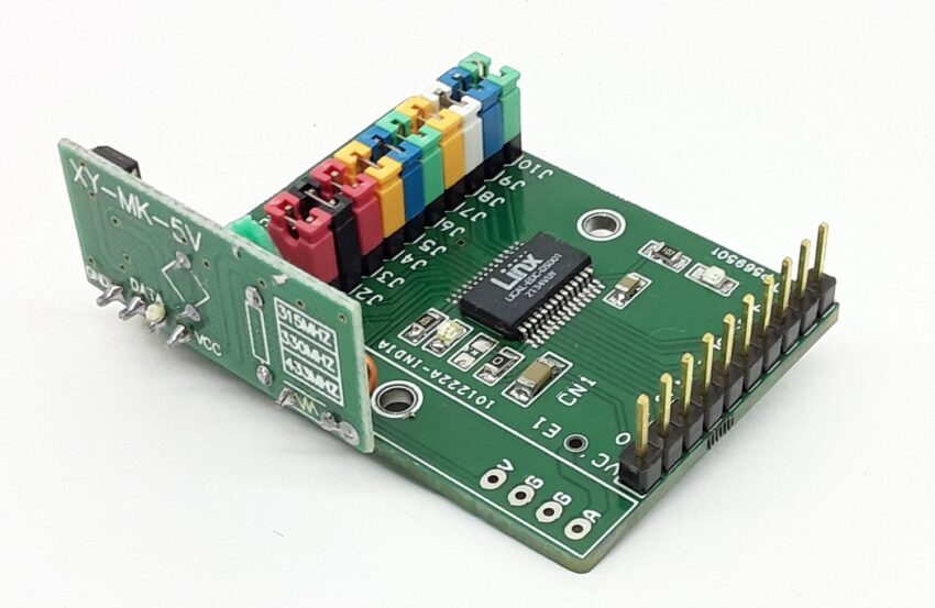
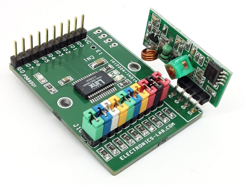
The project described here is 8 Channel RF Remote Receiver (Decoder). This 8-channel decoder is built using LICAL-EDC-DS001 chip from LINX. The board consists of the encoder/Decoder chip, 433Mhz RF Receiver module, and 10 x jumpers to set the address. Also, there is a header connector for data output which is ideal for controlling external devices, for example, relays. All outputs are compatible with TTL logic, normally they are low and go high when a valid signal is received and decoded by the chip. D2 onboard Power LED, D1 LED indicates valid transmission signal. All outputs are momentary (not latching)

 Features

  • Supply 5V DC
  • 10 Address Lines Selected through Jumpers J1 to J10
  • 8 Data Output TTL Compatible Normally Low (Momentary)
  • On Board Power LED
  • On Board VT LED (Valid Transmission)
  • PCB Dimensions 45.09 x 33.02 mm
  • 2 x 2.5mm Mounting Holes

System Configuration

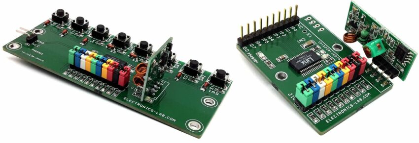
A simple remote-control system consists of an encoder, an RF transmitter, an RF receiver, and a decoder. The encoder is connected to 8 buttons, The encoder detects the closure of one of the switches and converts that into a digital data stream. This data is then sent to an RF transmitter that conveys this data into free space. An RF receiver receives the data and sends it to a decoder. The decoder analyses the data and, if it is valid, replicates the switch closure on an output. This output is then connected to whatever circuitry is to be controlled. All outputs are momentary and TTL logic.

remote control system (transmitter and receiver)

This DS series decoder and encoder chip is ideal for remote control applications. It decodes the signal received by 433 MHz RF modules. When the DS enters Decoder Mode, it checks the state of the DIN line. If it is high, the P_SEL line is checked to set which protocol is used and the decoder receives the data. It compares the address in the received packet to its local address lines. If they match, the data is stored and a second packet is received. With the Holtek® protocol, the decoder compares the two packets. If they match, the received data bits are output on the data lines and the VT line is pulled high thus LED D1 is on. This protocol compares each packet with the previous one looking for a match. The serial protocol requires two matching packets for initial activation, then updates the lines on each subsequent packet. The DS then looks for the next packet on the DIN line. With the Holtek® protocol, once no valid data is received (there is a mismatch of address, data, or bit timings), the Data and VT lines are pulled low and the DS goes to sleep until DIN is pulled high. The Serial protocol holds the output states until a 130ms timer runs out. The Holtek® protocol compares two packets and, if they match, sets the outputs. If a data line is toggled during a transmission (D1 is activated while D0 is already active) then the received packet does not match the previous packet and the output lines are pulled low until the next packet arrives. This causes all of the outputs to briefly cut out when a line is toggled. The serial protocol uses a timer to prevent this cutout.

LICAL-EDC-DS001 Encoder/Decoder Chip

The same part can be used as an encoder or decoder by selecting the state of one pin. The DS Series also has two protocols built into the same part, selected by the state of a single pin. One is compatible with Holtek devices, such as the HT640 and HT658. The other protocol is a serial data structure that is much more immune to noise and edge jitter. This protocol offers much more range and reliability than the Holtek protocol while keeping the simple jumper addressing.

Theory of Operation

The DS Series is a remote-control encoder and decoder that offers two protocols in one part based on the state of the P_SEL line. The first protocol operates with the Holtek® HT640 encoder and HT658 decoder. The second is a serial protocol that offers more noise immunity and faster response time while keeping the simple addressing. The DS can operate as either an encoder or decoder based on the state of the E/D_SEL line. It does not operate as both simultaneously. When set as an encoder it monitors the state of the TE line. When the line is high the DS records the states of the data and address lines, assembles them into a packet, and outputs the packet three times. The data lines can be connected to switches or contacts. The address lines can be set with Jumpers. When set as a decoder the DS receives packets and validates them. The validation includes checking the bit timings and comparing the received address to the local address line settings. Two matching packets must be received consecutively. If the timings are good and the addresses match, the DS sets its data lines to match the received states. These lines can be connected to the application circuitry to be controlled. When the TE/DIN line is low, the DS goes into a low-power sleep mode.

Setting the Address

The project has ten address lines. This allows the formation of up to 1,022 (210 – 2) unique transmitter-receiver relationships, Jumper J1 to J10 can be used to set the address, all lines are pulled high. The chip rejects packets with addresses set to all high or all low. At least one address line must be different from the rest. The encoder does transmit all addresses, but the decoder rejects packets with all address lines set the same. The receiver’s address line states must match the transmitter’s exactly for a transmission to be recognized. If the addresses do not match, then the decoder takes no action.

Initial Operation

On power-up, the E/D_SEL line is tested to determine if the DS operates as an encoder or a decoder. If the line is high, the DS enters Encoder Mode. If low, it enters Decoder Mode. This is checked once on power-up. Once the operating mode is selected, the data-line direction is set. In either mode, a rising edge on the TE/DIN line wakes the device from low-power sleep.

Connections and Other Information

  • Connections and Other Details
  • CN1: Pin 1 = VCC 5V In, Pin 2 = D0, Pin 3 = D1, Pin 4 = D2, Pin 5 = D3, Pin 6 = D4, Pin 7 = D5, Pin 8 = D6, Pin 9 = D7, Pin 10 GND
  • D1: Valid Signal LED
  • D2: Power LED
  • Jumper: J1 to J10 for Address Configuration
  • For Serial Protocol R2 = 0 Ohms, R3 Omit, For Holtek Protocol R3= 0 Ohms and R2 Omit (Read Data sheet of chip for Serial/Holtek Protocol)

Schematic

Parts List

NOQNTY.REFDESCMANUFACTURERSUPPLIERSUPPLIER PART NO
11CN18 PIN MALE HEADER PITCH 2.54MMWURTHDIGIKEY732-5321-ND
21C1100nF/25V CERAMIC SMD SIZE 0805MUARATA/YAGEODIGIKEY
31C210uF/16V CERAMIC SMD SIZE 1206MUARATA/YAGEODIGIKEY
41D1LED -GREEN SMD SIZE 0805DIALIGHTDIGIKEY350-2044-1-ND
51D2LED RED SMD SIZE 0805OSRAMDIGIKEY475-1278-1-ND
61E1ANTENNA/DNPDO NOT INSTALL
710J1-J10JUMPER/ 2 PIN MALE HEADER PITCH 2.54MMWURTHDIGIKEY732-5315
81M1RF AM RX MODULE 433MHZ.ALIEXPRESSALIEXPRESS
92R1,R141K/5% SMD SIZE 0805MUARATA/YAGEODIGIKEY
101R2DNP
111R30E SMD SIZE 0805MUARATA/YAGEODIGIKEY
1210R4-R13100K/5% SMD SIZE 0805MUARATA/YAGEODIGIKEY
131U1LICAL-EDC-DS001-TLINX TECHDIGIKEYLICAL-EDC-DS001-TCT-ND
1410SHUNTSHUNT FOR JUMPER J1 TO J10SULLINS CONNCTDIGIKEYS9001-ND

Connections


Gerber View

Photos

Video


LICAL-EDC-DS001 Datasheet

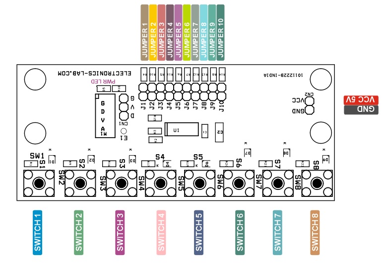
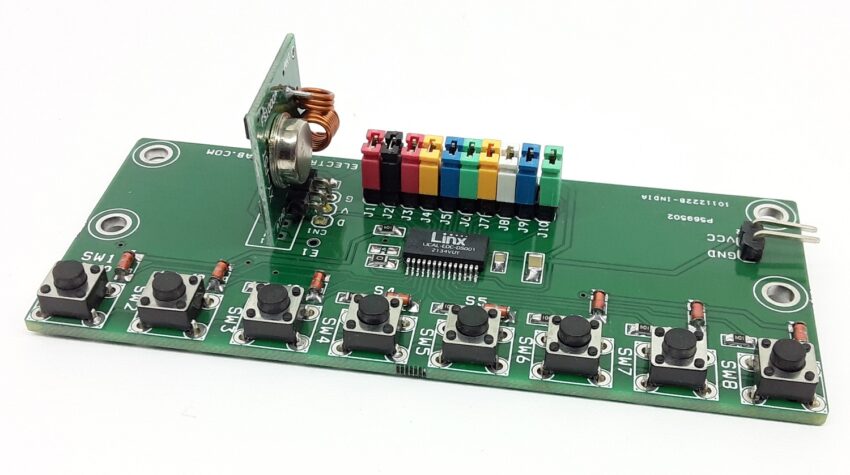
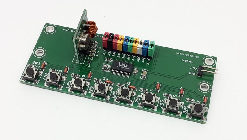
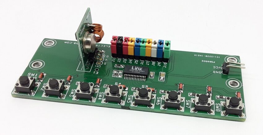
8 Channel RF Remote Transmitter with Holtek and Serial Protocol

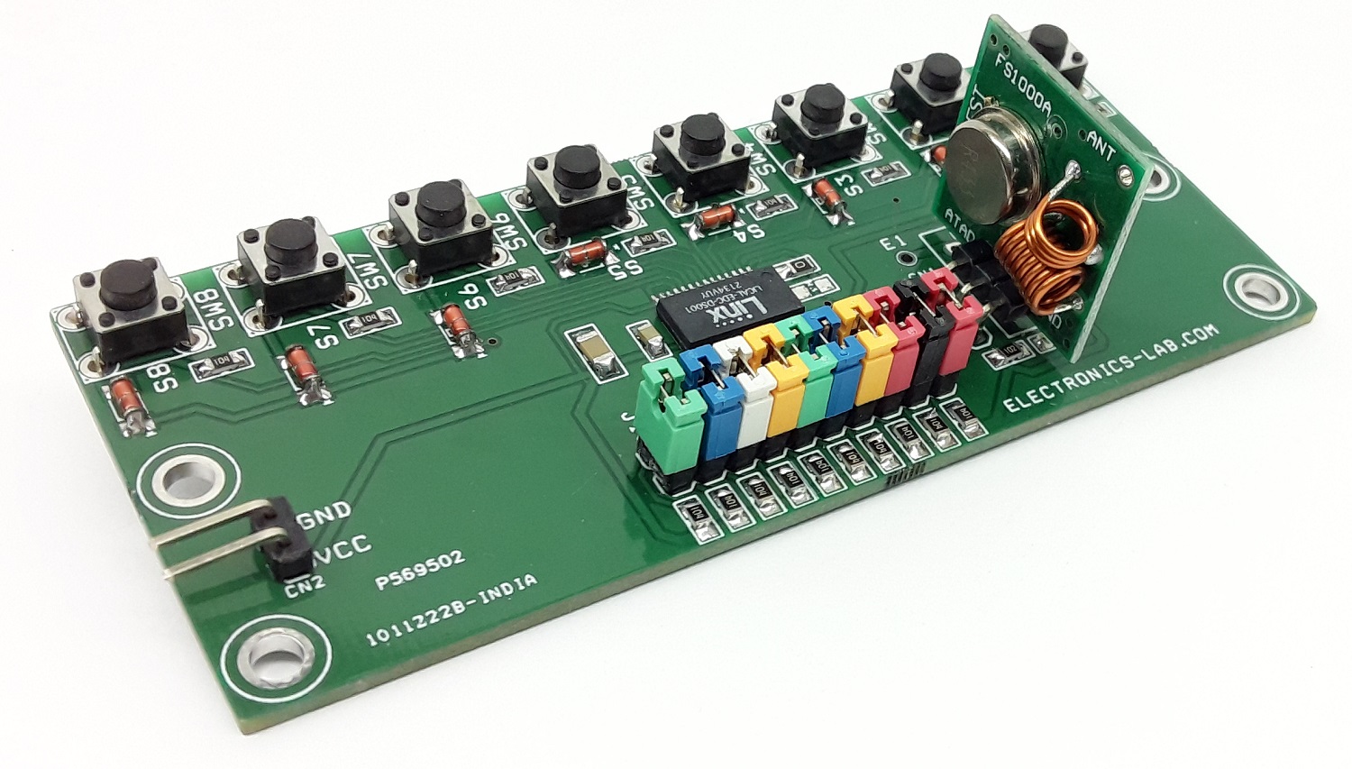
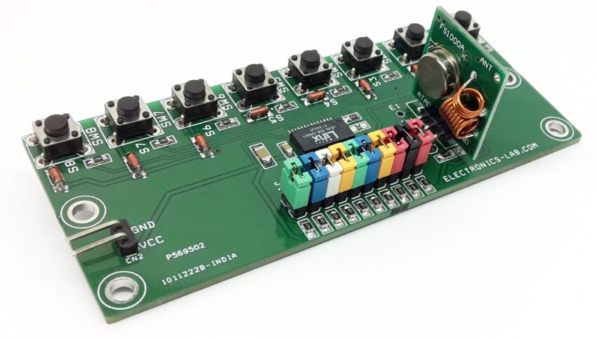
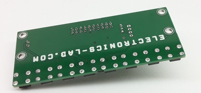
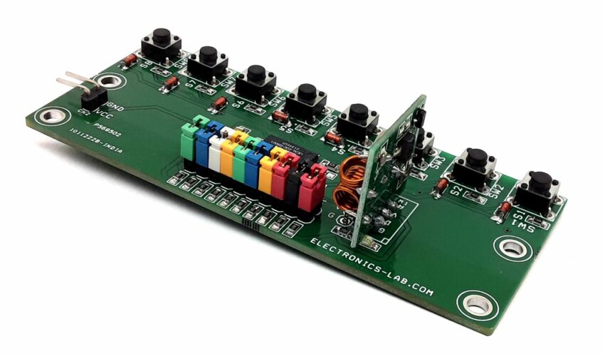
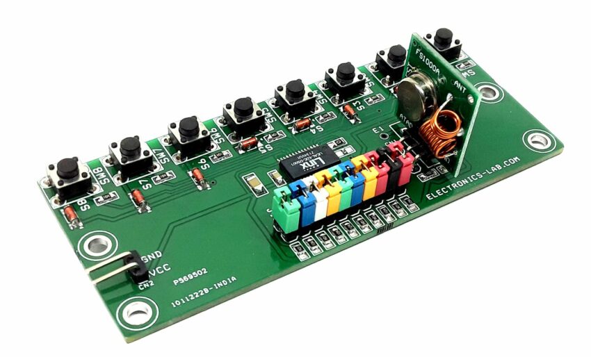
The project described here is an 8 Channel RF remote transmitter This transmitter is built using LICAL-EDC-DS001 chip from LINX. The project consists of the Encoder/Decoder chip, a 433Mhz RF module as a wireless link, 8 x tactile switches for operations, 10 x jumpers to set the transmitter address. This DS series decoder/encoder chip is ideal for remote control applications. It is able to transmit the status of up to 8 buttons across a wireless link. Addressing is accomplished by the logic state of 10 Jumpers J1 to J10.

Note: The project is compatible with the 8 Channel RF Remote Receiver and One Channel RF Remote Relay Switch published on our website.

LICAL-EDC-DS001 Encoder/Decoder Chip

The same part can be used as an encoder or decoder by setting the state of one pin. The DS Series also has two protocols built into the same part, selected by the state of a single pin. One is compatible with Holtek devices, such as the HT640 and HT658. The other protocol is a serial data structure that is much more immune to noise and edge jitter. This protocol offers much more range and reliability than the Holtek protocol while keeping the simple jumper addressing.

Theory of Operation

The DS Series is a remote-control encoder and decoder that offers two protocols in one part based on the state of the P_SEL line. The first protocol operates with the Holtek® HT640 encoder and HT658 decoder. The second is a serial protocol that offers more noise immunity and faster response time while keeping the simple addressing. The DS can operate as either an encoder or decoder based on the state of the E/D_SEL line. It does not operate as both simultaneously. When set as an encoder it monitors the state of the TE line. When the line is high the DS records the states of the data and address lines, assembles them into a packet, and outputs the packet three times. The data lines can be connected to switches or contacts. The address lines can be set with DIP switches or cut traces on a PCB. When set as a decoder the DS receives packets and validates them. The validation includes checking the bit timings and comparing the received address to the local address line settings. Two matching packets must be received consecutively. If the timings are good and the addresses match, the DS sets its data lines to match the received states. These lines can be connected to the application circuitry to be controlled. When the TE/DIN line is low, the DS goes into a low-power sleep mode.

remote control system (transmitter and receiver)

Setting the Address

The project has ten address lines. This allows the formation of up to 1,022 (210 – 2) unique transmitter-receiver relationships, Jumper J1 to J10 can be used to set the address, all lines are pulled high. The chip rejects packets with addresses set to all high or all low. At least one address line must be different from the rest. The encoder does transmit all addresses, but the decoder rejects packets with all address lines set the same. The receiver’s address line states must match the transmitter’s exactly for a transmission to be recognized. If the addresses do not match, then the decoder takes no action.

Initial Operation

On power-up, the E/D_SEL line is tested to determine if the DS operates as an encoder or a decoder. If the line is high, the DS enters Encoder Mode. If low, it enters Decoder Mode. This is checked once on power-up. Once the operating mode is selected, the data-line direction is set. In either mode, a rising edge on the TE/DIN line wakes the device from low-power sleep.

Encoder Mode

Once the chip enters Encoder Mode, it tests the state of the TE line. If it is high, the P_SEL line is checked to determine which protocol to use. Then the encoder records the states of the Data and Address lines and assembles a packet. When the Holtek® protocol is selected, the DS outputs the packet on the DOUT line three times. With the Serial protocol, it sends two packets, checking the states of the data lines each time. The second packet is the logical inversion of the first packet, ensuring a 50% duty cycle, which is an advantage for FCC testing. The DS then checks the state of the TE line again. It repeats this process for as long as the TE line is high. Once it goes low, the DS goes to sleep until TE is pulled high.

Decoder Mode

When the DS enters Decoder Mode, it checks the state of the DIN line. If it is high, the P_SEL line is checked to set which protocol is used and the decoder receives the data. It compares the address in the received packet to its local address lines. If they match, the data is stored and a second packet is received. With the Holtek® protocol, the decoder compares the two packets. If they match, the received data bits are output on the data lines and the VT line is pulled high. This protocol compares each packet with the previous one looking for a match. The serial protocol requires two matching packets for initial activation, then updates the lines on each subsequent packet. The DS then looks for the next packet on the DIN line. With the Holtek® protocol, once no valid data is received (there is a mismatch of address, data, or bit timings), the Data and VT lines are pulled low and the DS goes to sleep until DIN is pulled high. The Serial protocol holds the output states until a 130ms timer runs out. The Holtek® protocol compares two packets and, if they match, sets the outputs. If a data line is toggled during a transmission (D1 is activated while D0 is already active) then the received packet does not match the previous packet and the output lines are pulled low until the next packet arrives. This causes all of the outputs to briefly cut out when a line is toggled. The serial protocol uses a timer to prevent this cutout.

Note: The transmitter part is published here. The receiver part with multiple options will be published in the near future. The transmitter also can be used with Arduino + 433Mhz RF receiver module. Refer to the datasheet of the chip for more information about decoding the signal.

Connections and Other Information

  • Sw1 to Sw8 = Function Switches
  • CN2= PIN 1 = VCC 5V DC, PIN 2 = GND
  • Jumper J1 to J10 = For Address Configuration (should be the same for Transmitter and Receiver)
  • D5 Power LED
  • Transmitter PCB can accommodate 2 Types of RF Modules: 3 Pins CN1 or M1 4 Pin Module.
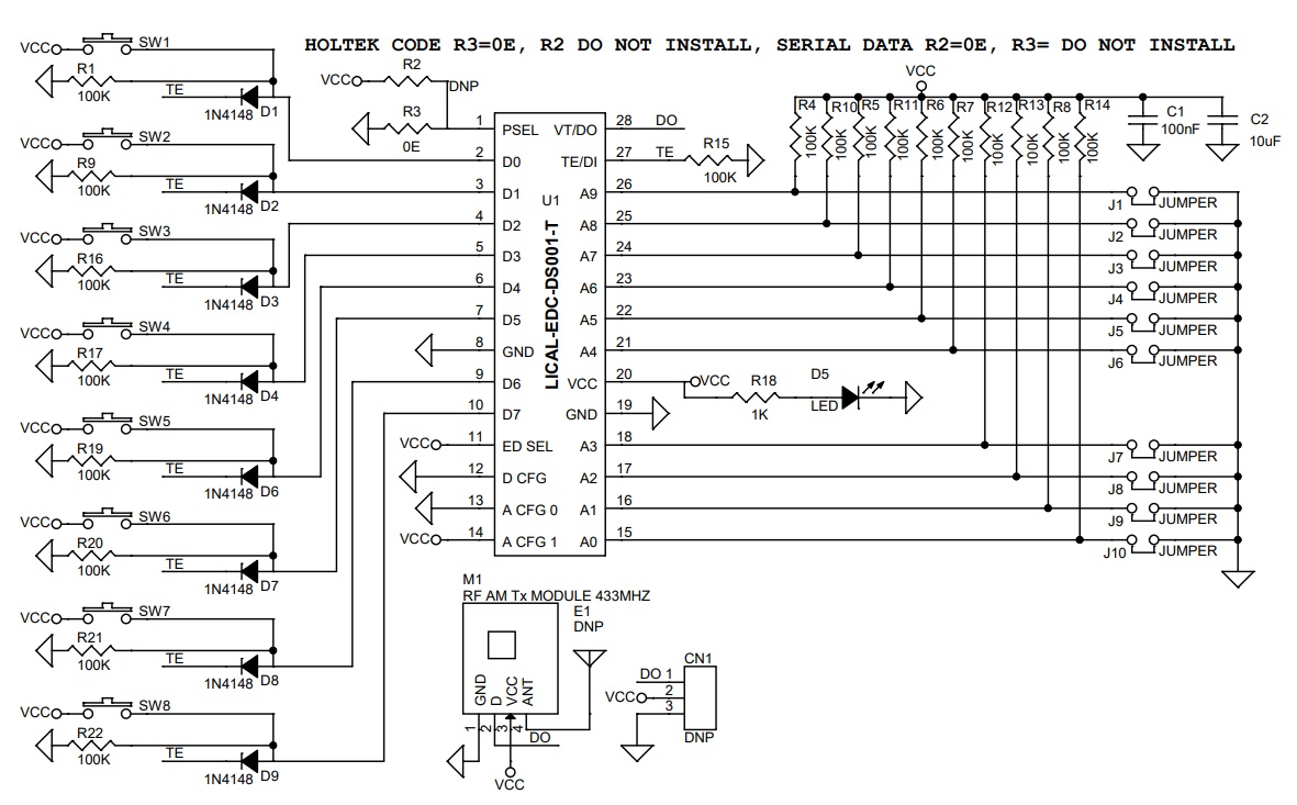
  • For Serial Protocol R2 = 0 Ohms, R3 Omit, For Holtek Protocol R3= 0 Ohms and R2 Omit (Read the datasheet of the chip for Serial/Holtek Protocol)

Features

  • Supply 5V DC
  • 10 Address Lines Selected through Jumpers J1 to J10
  • 8 X Tactile Switches (8 Data Lines)
  • On Board Power LED
  • PCB Dimensions 90.81 x 38.10 mm
  • 4 x 2.5MM Mounting Holes

Schematic

Parts List

NO.QNTY.REF.DESC.MANUFACTURERSUPPLIERSUPPLIER PART NO
13E1,CN1,R2DNP
21C1100nF/25V CERAMIC SMD SIZE 0805MUARATA/YAGEODIGIKEY
31C210uF/16V CERAMIC SMD SIZE 1206MUARATA/YAGEODIGIKEY
48D1 to D91N4148 SMD ONSEMIDIGIKEYLL4148FSCT-ND
51D5LED RED SMD SIZE 0805OSRAMDIGIKEY475-1278-1-ND
610J1 to J10JUMPER/ MALE HEADER PITCH 2.54MMWURTHDIGIKEY732-5315-ND
71M1RF AM Tx MODULE 433MHZALIEXPRESSALIEXPRESS
819R1,R4 to R22100K/5% SMD SIZE 0805MUARATA/YAGEODIGIKEY
91R30E SMD SIZE 0805MUARATA/YAGEODIGIKEY
101R181K/5% SMD SIZE 0805MUARATA/YAGEODIGIKEY
118SW1 to SW84PIN TACTILE SWITCHNKK SWITCHDIGIKEYHP0215AFKP2-ND
121U1LICAL-EDC-DS001-TLINX TECHDIGIKEYLICAL-EDC-DS001-TCT-ND

Connections

Gerber View

Photos

Video


LICAL-EDC-DS001 Datasheet

Universal Instrumentation Amplifier Module for SOIC8 Package with On-Board Reference

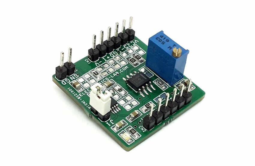
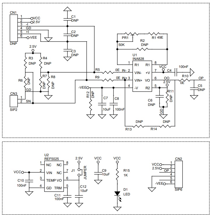
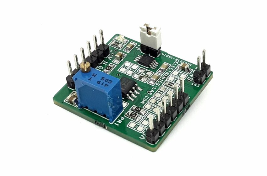
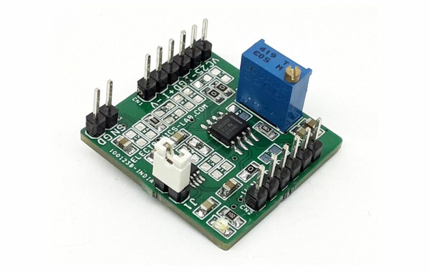
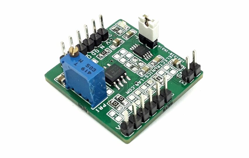
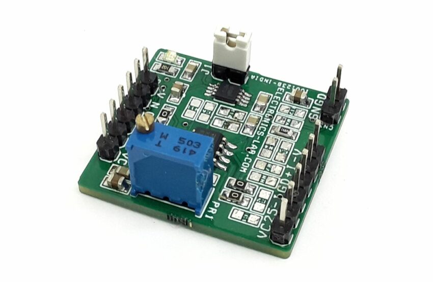
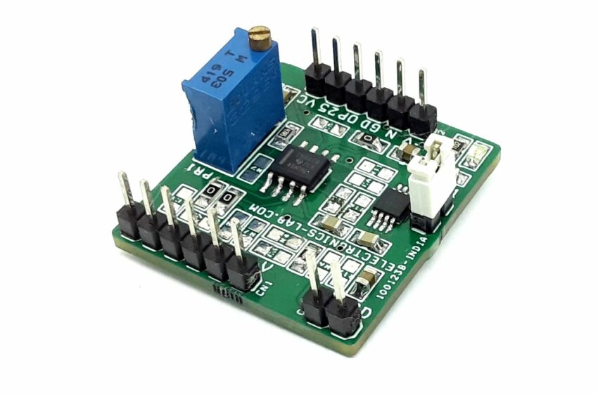
This is a universal instrumentation amplifier module for SOIC8 package. Various configurations are possible by selecting the right components. The board helps users to develop instrumentation amplifier circuits and it can accommodate SOIC8 devices such as INA828 from Texas Instruments. All capacitors are ceramic type size 0805 and resistors are also size 0805. It supports dual supply or single supply, install R12 0 Ohms for a single supply usage. Various capacitors and resistors can be installed as per application requirements. D1 is the Power LED. Board also has 2.5V precision reference voltage chip. Jumper J1 is provided to select the 2.5V reference voltage to the IN828 Amplifier.  An external reference voltage can be fed through CN1 or CN2 Pin 2, Open Jumper J1 in this case. The project also consists of resistors R3, R4, R7, and R8 to create bridge configurations for various sensors. CN3 is provided for sensor input.

Note: The project consists of bridge configuration circuitry which helps with various sensor interfaces. Install R3, R4, R7, and R8 as per requirement and use CN3 for Sensor input.

Features

  • Single Supply: 4.5 V to 36 V, Dual Supply: ±2.25 V to ±18 V
  • On Board Reference Voltage Generator Chip (Available Reference 2.5V, 5V, 1.2V)
  • On Board Power LED
  • On Board Jumper J1 for Reference Voltage Selection, External or Internal
  • Header Connector for Inputs, Outputs, and Supply
  • Gain Adjustable 1 to 1000 Using Multiturn Trimmer Potentiometer
  • PCB Dimensions 29.05 x 27.31 mm

Applications

  • Bridge Amplifiers
  • ECG Amplifiers
  • Pressure Sensors
  • Medical Instrumentation
  • Portable Instrumentation
  • Weigh Scales
  • Thermocouple Amplifiers
  • RTD Sensor Amplifiers
  • Data Acquisition

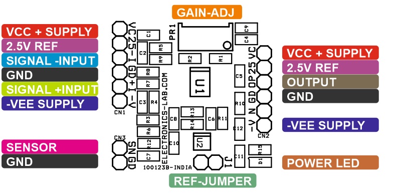
Connections and Other Details

  • CN1: Pin1=VCC, Pin2=Voltage Reference 2.5V, Pin3= -Signal Input, Pin4=GND, Pin5= +Signal Input, Pin5=-VEE Supply Input
  • CN2: Pin1=VCC + Supply, Pin2=Voltage Reference 2.5V, Pin3= Output, Pin4=GND, Pin5= NC, Pin5=-VEE Supply
  • CN3: Sensor Input for Bridge Configuration
  • PR1: Multi-Turn Potentiometer for Gain Adjust (Gain 1 to 1000)
  • J1: External or Internal Reference Selection (Internal Reference 2.5V)
  • D1: Power LED

Schematic

Parts List

NOQNTYREF.DESCMANUFACTURERSUPPLIERSUPPLIER PART NO
11CN1,CN26 PIN MALE HEADER PITCH 2.54MMWURTHDIGIKEY732-5319-ND
22CN32 PIN MALE HEADER PITCH 2.54MMWURTHDIGIKEY732-5315-ND
313R1,R3,R4,C1,R2,C2,C3,C5,R6,C6,C8,R11,R12,R13,R14,R8DNP/AS PER USER REQUIRMENT DIGIKEY
45C4,C8,C9,C10,C11100nF/50V CERAMIC SMD SIZE 0805YAGEO/MURATADIGIKEY
51SHUNT FOR JUMPER-J1SHUNTSULLINS CONNCTDIGIKEYS9001-ND
62C7,C1210uF/25V CERAMIC SMD SIZE 0805YAGEO/MURATADIGIKEY
71D1LED RED SMD SIZE 0805OSRAMDIGIKEY475-1278-1-ND
81J1JUMPER/2PIN MALE HEADER 2.54MMWURTHDIGIKEY732-5315-ND
91PR150K MULTI TURN POTBOURNSDIGIKEY3296W-503LF-ND
103R5,R9,R100E SMD SIZE 0805YAGEO/MURATADIGIKEY
111R149.9E 1% SMD SIZE 0805YAGEO/MURATADIGIKEY
121R151K 5% SMD SIZE 0805YAGEO/MURATADIGIKEY
131U1INA828 SOIC8TIDIGIKEY296-48914-1-ND
141U2REF5025 VSSOP8TIDIGIKEY296-24499-1-ND

Connections

Gerber View

Photos

Video

INA828 Datasheet

Universal Instrumentation Amplifier Module for VSSOP8 Package with On-Board Reference

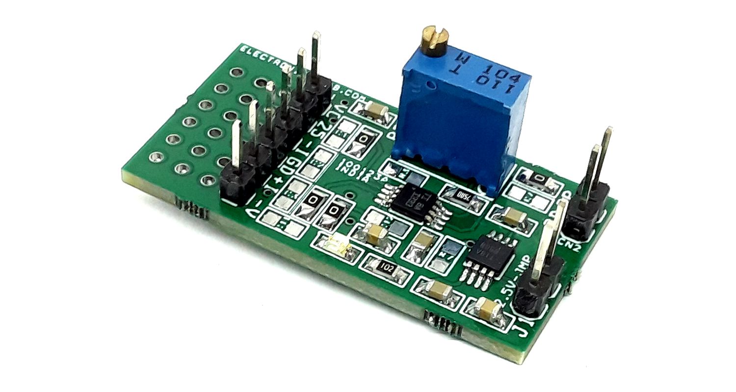
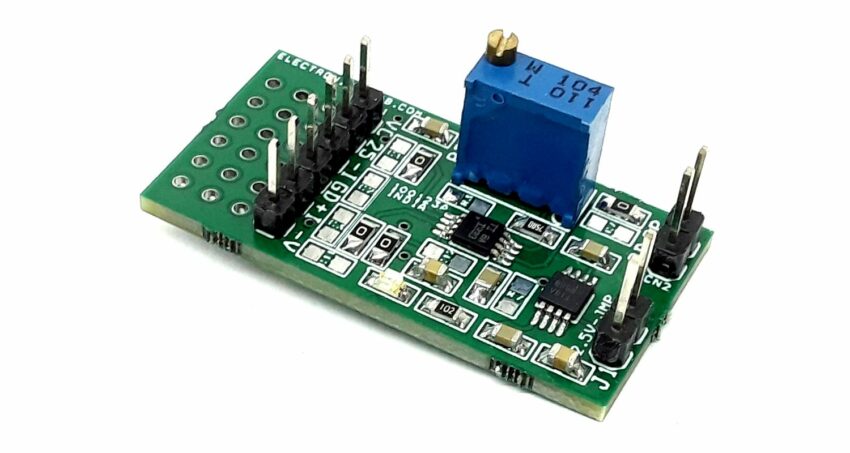
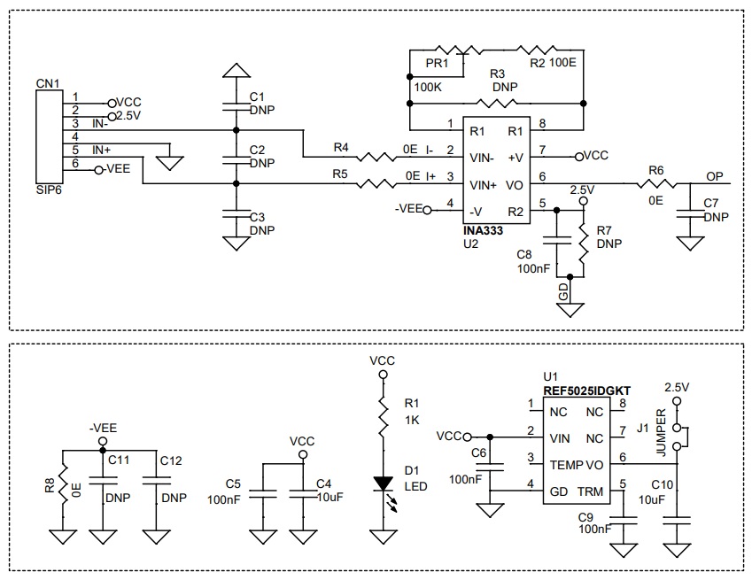
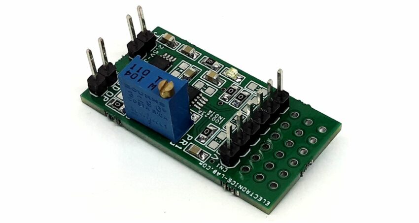
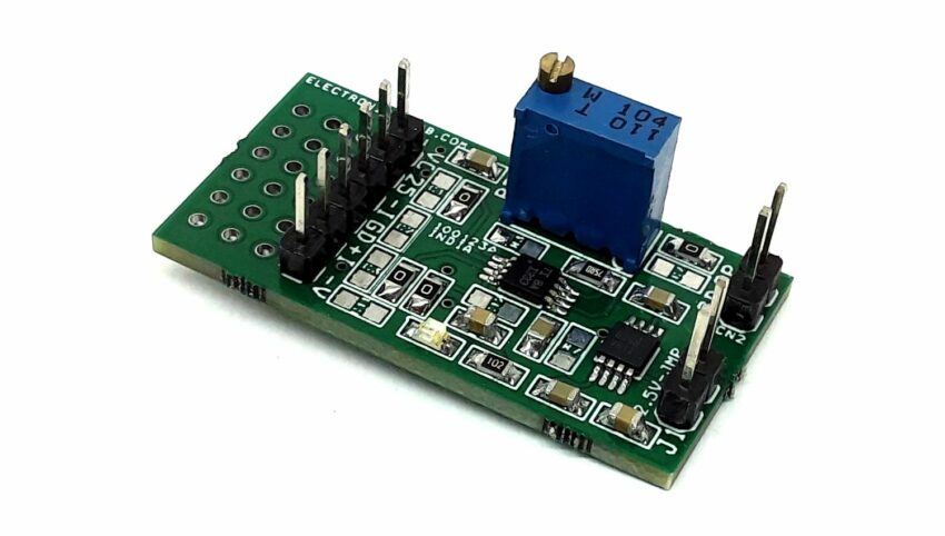
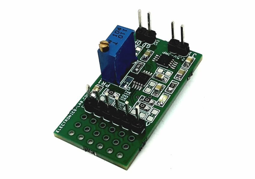
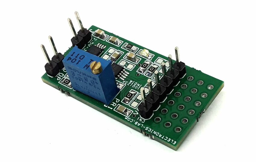
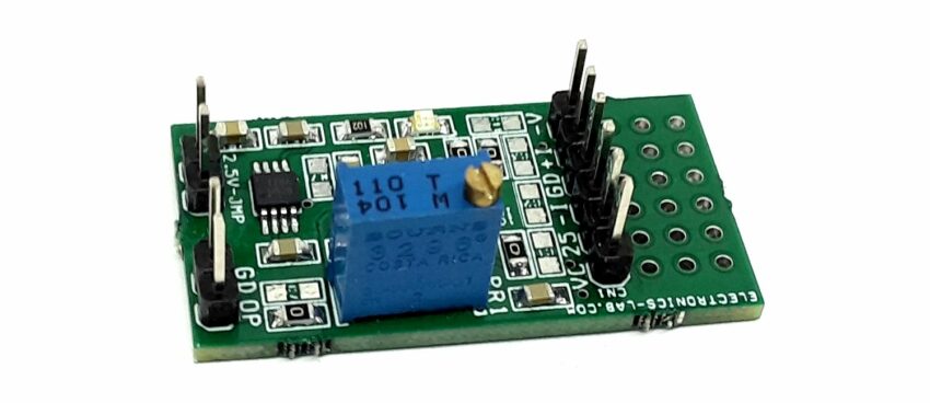
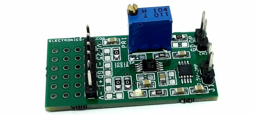
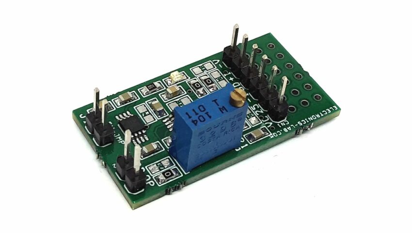
This is a universal instrumentation amplifier module that can be used to develop and test instrumentation amplifier circuits. The board can accommodate VSSOP8 devices such as INA126, INA333, INA155, INA156 from Texas Instruments. All capacitors are ceramic type with size 0805 and resistor size is also 0805. It supports dual supply or single supply. You should install R8 0 Ohms for a single supply usage. Various capacitors and resistors can be installed as per application requirements. D1 Power LED. Board has also a 2.5V precision reference voltage chip. Jumper J1 is provided to select the 2.5V reference voltage to the INA333 Amplifier. An external reference voltage can be fed through CN1 Pin 2. In this case Open Jumper J1. Also, a small prototyping area is provided.

Note: The board can be used with various amplifiers such as INA126, INA333, INA155, and INA156

Features

  • Single Supply 5V DC for INA333 (Range 1.8V to 5.5V), Single Supply: 4.5 V to 36 V, Dual Supply: ±2.25 V to ±18 V
  • On Board Reference Voltage Generator Chip (Available Reference 2.5V, 5V, 1.2V)
  • On Board Power LED
  • On Board Jumper J1 for Reference Voltage Selection, External or Internal
  • Header Connector for Inputs, Outputs, and Supply
  • Small Prototype Area Provided
  • Gain Adjustable 1 to 1000 Using Multiturn Trimmer Potentiometer
  • PCB Dimensions 37.15 x 19.21 mm

Applications

  • Bridge Amplifiers
  • ECG Amplifiers
  • Pressure Sensors
  • Medical Instrumentation
  • Portable Instrumentation
  • Weigh Scales
  • Thermocouple Amplifiers
  • RTD Sensor Amplifiers
  • Data Acquisition

Connections and Other Details

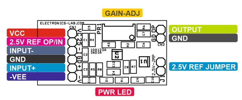
  • CN 1: Pin 1=VCC, Pin2=2.5V Ref Out, Pin3=Signal -Input, Pin4=GND, Pin5=Signal +input, Pin6=-VEE
  • PR1: Gain Adjust Multiturn Pot 1 To 1000
  • D1: Power LED
  • Jumper J1: Internal Reference 2.5V Selection, Open for External Reference Input
  • U1: Reference Voltage Generator 2.5V Output
  • Resistor R8: Use 0Ohms for Single Supply, Open for Dual Supply Input

Schematic

Parts List

NO.QNTY.DESC.REF.MANUFACTURERSUPPLIERSUPPLIER PART NO
11CN16 PIN MALE HEADER PITCH 2.54MMWURTH732-5319-ND
28C1,C2,C3,R7,C7,C11,C12,R3DNP/AS PER USER REQUIRMENT
32C4,C1010uF/16V CERMIC SMD SIZE 0805MURATA/YAGEO
44C5,C6,C8,C9100nF/50V CERAMIC SMD SIZE 0805MURATA/YAGEO
61D1LED RED SMD SIZE 0805OSRAM475-1278-1-ND
71J1JUMPER- 2 PIN MALE HEADER PITCH 2.54MMWURTH732-5315-ND
81PR1100K MULTITURN TRIMMER POTBOURNS3296W-1-104
91R11K 5% SMD SIZE 0805MURATA/YAGEO
101R2100E 1% SMD SIZE 0805MURATA/YAGEO
124R4,R5,R6,R80E SMD SIZE 0805MURATA/YAGEO
131U1REF5025IDGKT 8VSSOPTI296-24499-1-ND
141U2INA333 8VSSOPTI296-23564-1-ND
151J1-SHUNTSHUNT FOR JUMPER J1SULLINS CONNECTS9001-ND

Connections

Gerber View

Photos

Video

INA333 Datasheet

Introducing the New ESP32-S3 with Camera

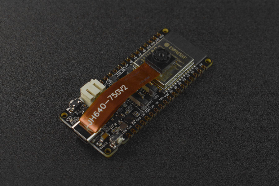
FireBeetle 2 Board ESP32-S3 (N16R8) AIoT Microcontroller with Camera (Supports Wi-Fi & Bluetooth)

FireBeetle 2 ESP32-S3 is a high-performance main controller built around the ESP32-S3-WROOM-1-N16R8 module. ESP32-S3-WROOM-1-N16R8 comes with 16MB Flash and 8MB PSRAM for storing more data. The acceleration for neural network computing and signal processing workloads provided by the ESP32-S3 chip makes the module an ideal choice for a wide variety of applications, such as speech recognition, image recognition, and so on.

Specifications

Basic Parameters

  • Operating Voltage: 3.3V
  • Type-C Input Voltage: 5V DC
  • VCC Input Voltage: 5V DC
  • Max Charging Current: 1A
  • Operating Temperature: -20 to 70℃
  • Dimension: 25.4x60mm/1×2.36”

Hardware Information

  • Processor: Xtensa® dual-core 32-bit LX7 microprocessor
  • Main Frequency: 240 MHz
  • SRAM: 512KB
  • ROM: 384KB
  • Flash: 16MB
  • PSRAM: 8MB
  • RTC SRAM: 16KB
  • USB: USB 2.0 OTG full-speed

WIFI

  • WIFI Protocol: IEEE 802.11b/g/n
  • Bandwidth: Support 20 MHz and 40 MHz at 2.4 GHz band
  • WIFI Mode: Station, SoftAP, SoftAP+Station combined mode
  • WIFI Frequency: 2.4GHz
  • Frame Aggregation: TX/RX A-MPDU, TX/RX A-MSDU

Bluetooth

  • Bluetooth Protocol: Bluetooth 5, Bluetooth mesh
  • Bluetooth Frequency: 125 Kbps, 500 Kbps, 1 Mbps, 2 Mbps

Ports

  • Digital I/O x26
  • LED PWM Controller 8 Channels
  • SPI x4
  • UART x3
  • I2C x2
  • I2S x2
  • IR Transceiver: transmit channel x5, receive channel x5
  • 2×12-bit SAR ADC, 20 Channels
  • DMA Controller: transmit channel x5, receive channel x5

FireBeetle 2 ESP32-S3 offers an onboard camera interface for easy connection with a camera. Also, an independent camera power supply circuit is designed, which helps reduce interference from other signals to the camera. The board comes with an OV2640 camera that offers 2 megapixels, 68° FOV, and up to 1600*1200 resolution. Besides, its onboard, easy-to-connect GDI greatly saves the trouble of wiring for using with a screen. Meanwhile, the controller integrates a power management function, which allows users to charge a Li-ion battery and turn the hardware on/off.

Features

  • ESP32-S3 module with AI Acceleration
  • 16MB Flash & 8MB PSRAM, more storage space
  • Onboard camera interface & independent camera power supply, easy to connect and strong anti-interference
  • Power management integrated, support Li-ion battery charging and hardware On/OFF controlling
  • Onboard GDI for easy connection with screens
  • Wi-Fi and Bluetooth 5 dual-mode communication

In addition, FireBeetle 2 ESP32-S3 supports WiFi and Bluetooth 5 (LE) dual-mode communication, which reduces the difficulty of networking. Meanwhile, both Bluetooth Mesh protocol and Espressif WiFi Mesh are supported for more stable communication and a larger coverage area. With the support of Matter protocol, the microcontroller can be used to develop industrial standard smart home devices for a wider range of IoT and AIoT (Artificial Intelligence of Things)scenarios.

FireBeetle 2 ESP32-S3 can be programmed by Arduino IDE, ESP-IDF, and MicroPython. Both C and Python are supported.

Documents

Raspberry Pi Fleet Management with Qbee

A smart approach to tackle device management

In recent years, the popularity of Raspberry Pi has shot up, leading to a growing demand for efficient device management solutions. Currently, some solutions available for device management include:

  • Automated SSH logins
  • Pre-built image with adequate security measures in place.
  • Device management software/system.

The optimum choice, according to studies, is to employ a pull-and-state-based device management solutions. Interestingly pull and state-based systems ensure devices stay updated even during offline periods – and that the device will always remain at the desired functional level – regardless of when it was added to the system or last seen.

Qbee.io delivers an intuitive SaaS IoT device management platform that supports over-the-air (OTA) software updates and remote scripting for most embedded Linux devices, be it a single Raspberry Pi or fleets of business-grade edge devices. With automated IoT device administration and dynamic remote VPN access, a UI-based solution gives users complete control over their device deployments. This all-inclusive solution provides remote scripting, monitoring, over-the-air software updates, and remote access. Qbee’s user-friendly UI makes IoT device management solutions more accessible and allows users to focus on enhancing their core product.

Advanced Features

In addition to IoT device management, Qbee offers a host of other advanced features. Here’s a comprehensive list of Qbee’s true potential:

IoT Configuration Management

This is a great way to automate Linux systems with IoT configuration management. QBee’s built-in automation is incredibly useful for managing various aspects of the system, such as users, passwords, firewalls, NTP servers, package or software updates, ssh keys, and more. The advanced file distribution feature enables the distribution of files, certificates, and the execution of scripts. This product offers a comprehensive group policy feature that allows fleet devices to quickly obtain common or individual configurations, with the added benefit of templating options. The REST API allows easy integration with third-party systems, providing access to all configuration settings.

Security & Linux Hardening

Qbee provides extensive Linux hardening and security features that safeguard devices. This configuration management tool is highly effective in securely distributing ssh keys, managing user and password security, and ensuring optimal firewall settings. This tool keeps libraries up-to-date and conducts continuous CVE vulnerability scans on all Linux packages. It makes it easy to detect potential security issues and take action before any damage occurs.

IoT Remote Control

The SaaS solution offers a centralized platform to control a Raspberry Pi, industrial gateway, or any other Linux-based device. The web-based ssh shell and qbee-connect desktop tool are great ways for mapping remote ports to localhost. This makes it simple to use third-party applications like Node-RED. This feature enables VNC, WinSCP, and connection to SCADA systems, making it a versatile tool.

IoT OTA Software Update

With the constant evolution of applications and the Linux OS, IoT OTA updates, and a Docker orchestration engine are becoming increasingly essential. Qbee provides an easy, safe, and expandable way to distribute updates through a file manager, repository, or a CI/CD setup by utilizing  REST API to integrate with third-party services like Github or other platforms.

IoT Device Monitoring

Qbee is an amazing IoT device monitoring solution that gathers all the necessary metrics, such as software inventories, port usage, docker container status, connectivity, operational status, and more. Analysis tools are a great resource to quickly identify and resolve memory leaks, stalling processes, or network inconsistencies, allowing users to seamlessly optimize performance and minimize downtime.

Remote Scripting

Users can efficiently distribute and execute scripts on multiple devices remotely. Qbee’s “command to run” function is designed to trigger a new script to run as soon as a change in the script is detected. Additionally, the feedback loop feature makes it easy to track the output of any operation. Advanced templating makes it easy to configure and execute remote commands or run advanced scripts with post commands and in-order execution on a group or individual device level.

In a nutshell, Qbee manages IoT edge devices properly and it offers,

  • IoT device management
  • Remote access VPN
  • Templated remote scripts
  • CVE vulnerability analysis
  • Github integration – CI / CD
  • Performance monitoring
  • A user-friendly UI & REST API
  • Zero development
  • Docker container management

Purchase Plan information:

All plans begin with a 14-day trial. You can sign up for Qbee on a monthly or annual basis – the latter offering a 10% discount. The free account enables users to connect two devices, whereas the paid ones include up to 20 devices. When it comes to pricing, Qbee offers a Startup plan (test and launch your IoT ideas) and a Pro plan – each one costing $89/ month and $269/ month, respectively. The Premium plan involves getting a price quote from the company and comes with a multitude of options, such as an SLA and personal account manager.

TOP PCB Companies