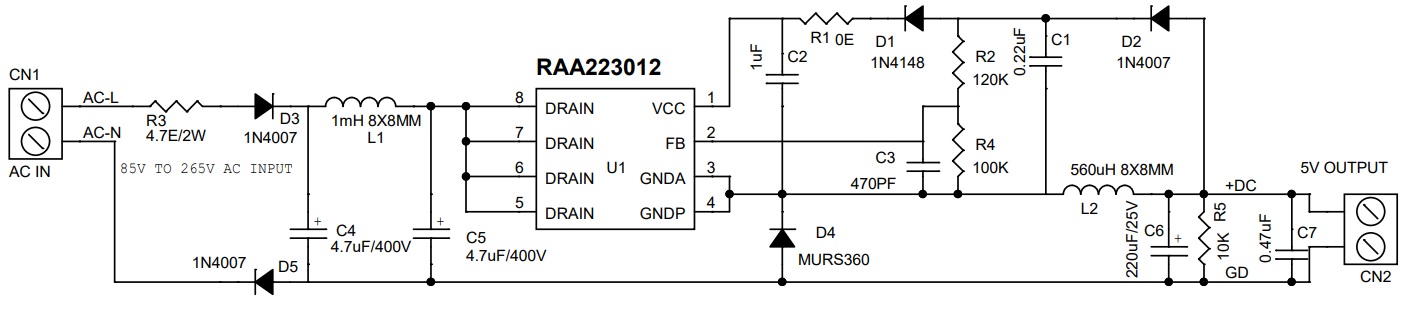
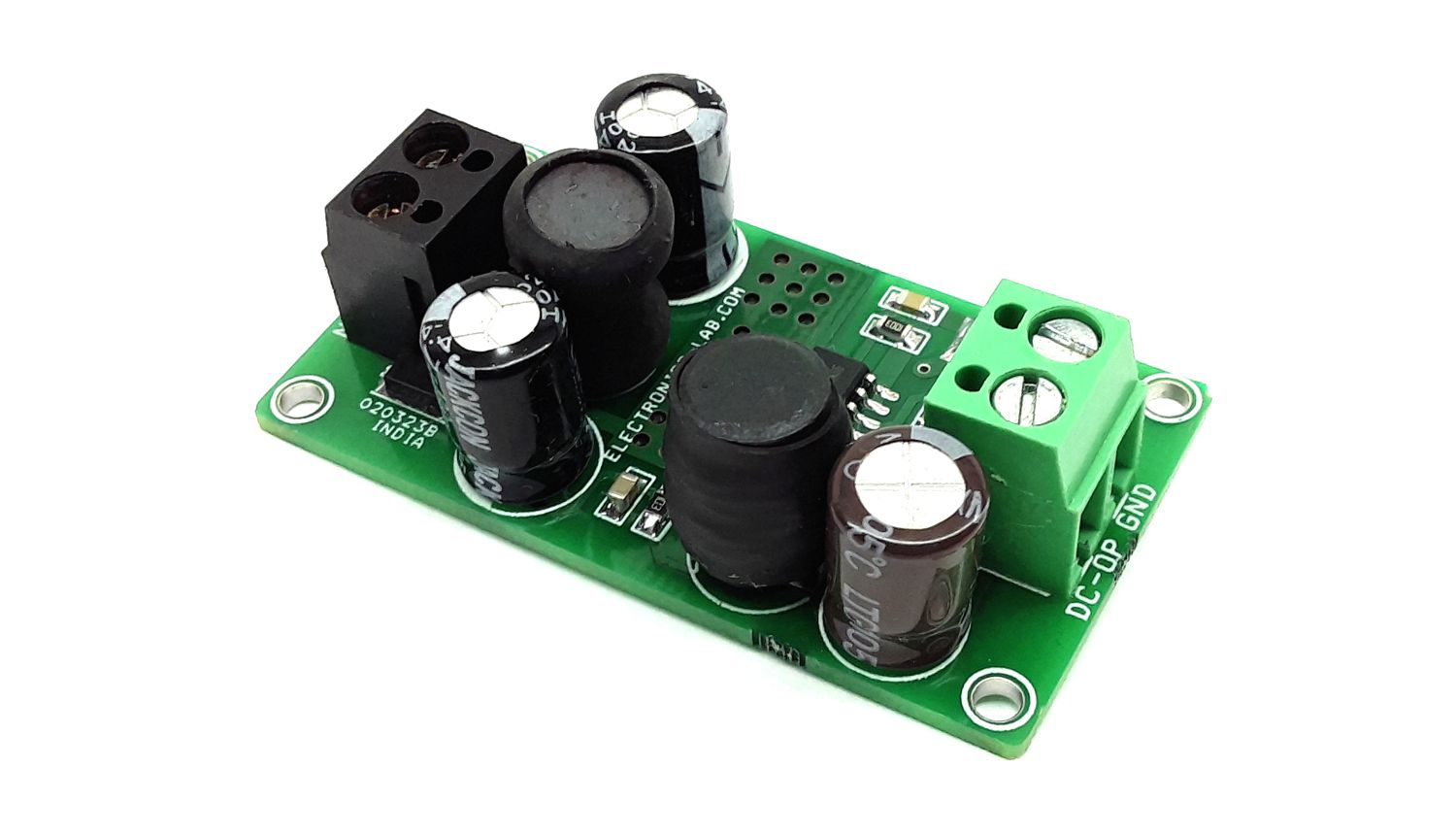
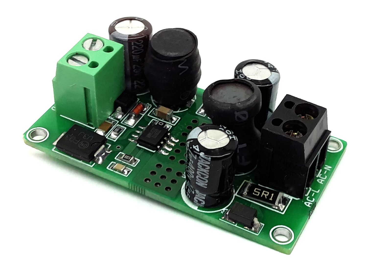
The project presented here is a universal input AC/DC switching buck regulator with ultra-low standby power that is capable of delivering up to 2.5W output power. The RAA223012 chip is the heart of the project which combines constant off-time control for heavy load and Pulse Frequency Modulation (PFM) for light-load operation. Constant off-time controls switching frequency above the audible frequency of approximately 50kHz. PFM eliminates any potential audible noises while offering superior light-load efficiency and ultra-low power consumption (<10mW at no load). Efficiency is achieved up to 75%. The built-in frequency dithering further reduces the EMI noise spectrum. The RAA223012 also features input brownout protection that prevents input circuitry from the overcurrent at low input voltage, and hiccup protections for output fault conditions such as short-circuit, overload, and open feedback.
Features
- Universal Input 85V to 265V AC 50/60Hz
- Output 5V DC, 150mA
- Output Short Circuit Protection
- Overload Protection (OLP)
- Short-Circuit Protection (SCP)
- Open Feedback Protection
- Over-Temperature Protection (OTP)
- 4 x 2.5mm Mounting Holes
- PCB dimensions 52.07 x 28.58 mm
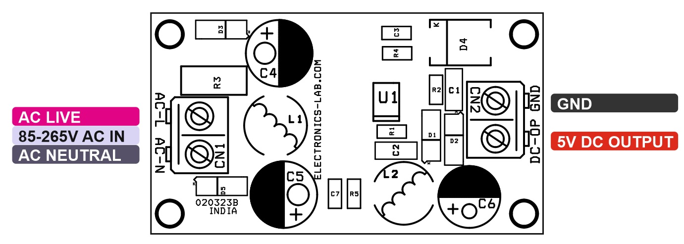
Connections And Other Details
- CN1: Pin 1 = AC Live Input, Pin 2 = AC Neutral Input (85V to 265V AC Range)
- CN2: Pin 1 = +5V DC Output, Pin 2 = GND
Short-Circuit Protection
When the output is shorted, VOUT = 0, VFB drops to zero because of the feedback network, introducing a delay. Before VFB drops to VFB_TOFFMIN, the RAA223012 operates with TONMAX and TOFFMIN, which quickly builds up a high current (>IPK) because the inductor peak current does not get reset. When the current reaches ISC_TH, a timer is started. If the inductor current reaches ISC_TH for four consecutive cycles, the RAA223012 determines that a short-circuit is present and immediately shuts off the switching. The IC then quickly charges VCC up to 5.9V and discharges it with a 19µA current source to 3.4V. When VCC drops to 3.4V, a 1.6mA current source charges VCC back to 5.9V where the IC resumes switching. When the RAA223012 resumes switching, assuming VFB drops to zero, the IC operates with the increased TOFFMIN_MAX so the inductor current can fully reset below the maximum peak limit. The RAA223012 operates in CCM with the inductor peak current being limited at IPK, with an average current around 240mA during the short. The part remains in hiccup mode until the short is removed. When the short is removed, VOUT returns to normal.
Schematic
Parts List
| NO | QNTY | REF. | DESC | MANUFACTURER | SUPPLIER | SUPPLIER'S PART NO |
|---|---|---|---|---|---|---|
| 1 | 1 | CN1 | 2 PIN SCREW TERMINAL PITCH 5.08MM | PHOENIX | DIGIKEY | 277-1247-ND |
| 2 | 1 | CN2 | 2 PIN SCREW TERMINAL PITCH 5.08MM | PHOENIX | DIGIKEY | 277-1247-ND |
| 3 | 1 | C1 | 0.22uF/25V CERAMIC SMD SIZE 1206 | YAGEO/MURATA | DIGIKEY | |
| 4 | 1 | C2 | 1uF/25V CERAMIC SMD SIZE 1206 | YAGEO/MURATA | DIGIKEY | |
| 5 | 1 | C3 | 470PF/50V CERAMIC SMD SIZE 0805 | YAGEO/MURATA | DIGIKEY | |
| 6 | 2 | C4,C5 | 4.7uF/400V | WURTH | DIGIKEY | 732-8689-3-ND |
| 7 | 1 | C6 | 220uF/25V | PANASONIC | DIGIKEY | P10271-ND |
| 8 | 1 | C7 | 0.47uF/25V CERAMIC SMD SIZE 0805 | YAGEO/MURATA | DIGIKEY | |
| 9 | 1 | D1 | 1N4148 SMD | MICROCHIP | DIGIKEY | 1N4148UR-1-ND |
| 10 | 3 | D2,D3,D5 | 1N4007 SMD | DIODE INC. | DIGIKEY | S1MBDITR-ND |
| 11 | 1 | D4 | MURS360 SMD | DIODE INC. | DIGIKEY | 31-MURS360CT-ND |
| 12 | 1 | L1 | 1mH 8X8MM SMD OR THT | WURTH | DIGIKEY | 732-3261-ND |
| 13 | 1 | L2 | 560uH 8X8MM SMD OR THT | BOURNS | DIGIKEY | RLB0914-561KL-ND |
| 14 | 1 | R1 | 0E SMD SIZE 0805 | YAGEO/MURATA | DIGIKEY | |
| 15 | 1 | R2 | 120K 1% SMD SIZE 0805 | YAGEO/MURATA | DIGIKEY | |
| 16 | 1 | R3 | 4.7E OR 5.1E 2W 5% SMD 2512 | YAGEO/MURATA | DIGIKEY | |
| 17 | 1 | R4 | 100K 1% SMD SIZE 0805 | YAGEO/MURATA | DIGIKEY | |
| 18 | 1 | R5 | 10K 1% SMD SIZE 0805 | YAGEO/MURATA | DIGIKEY | |
| 19 | 1 | U1 | RAA223012 SOIC8 | RENESAS | DIGIKEY | 20-RAA2230124GSP#HA0CT-ND |
Connections
Gerber View
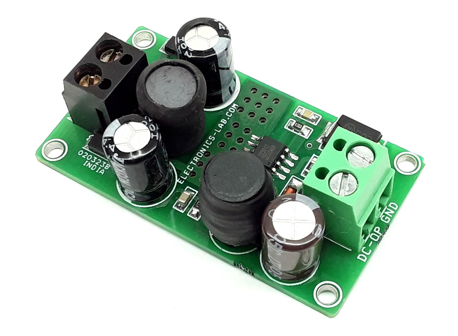
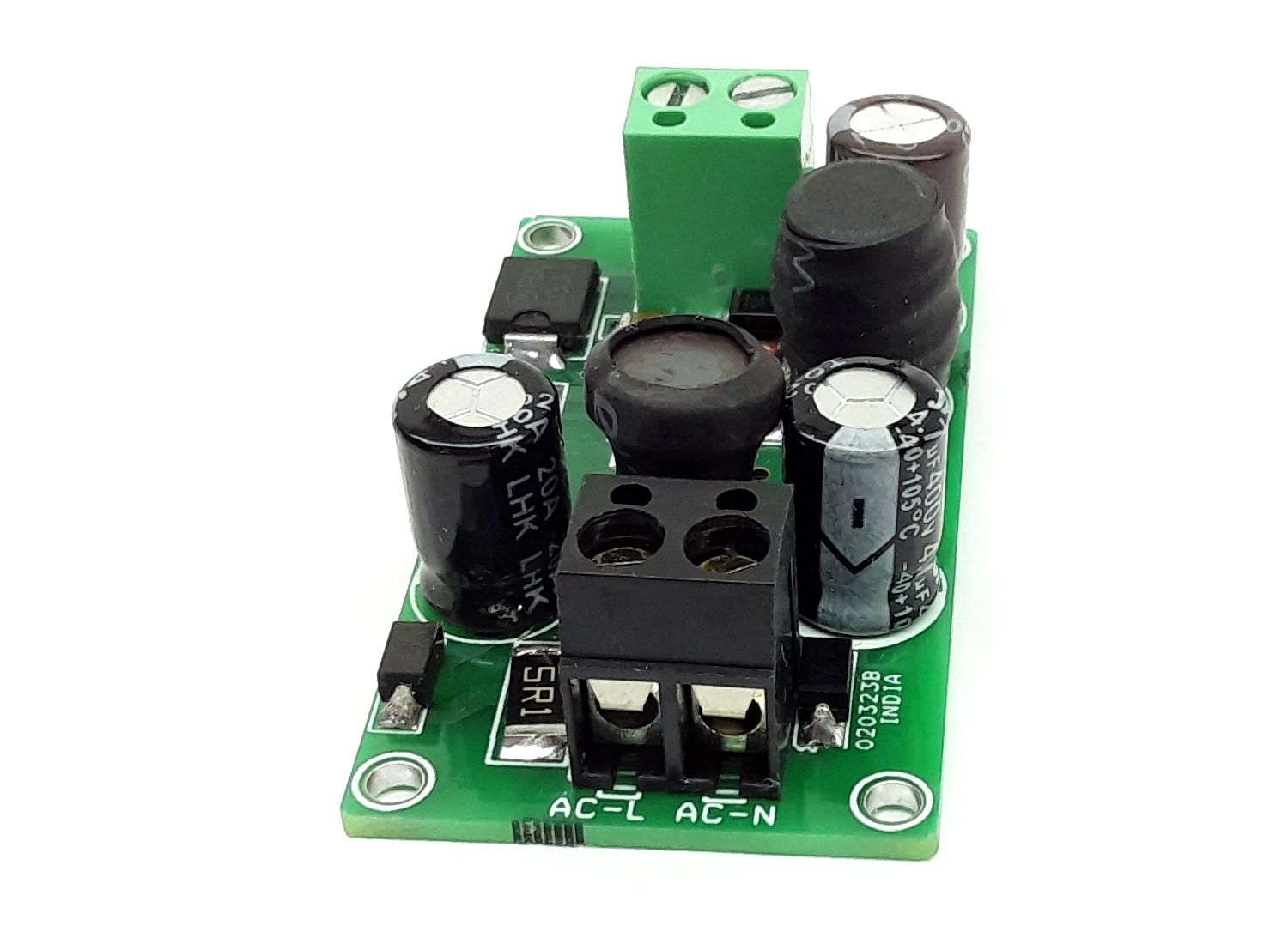
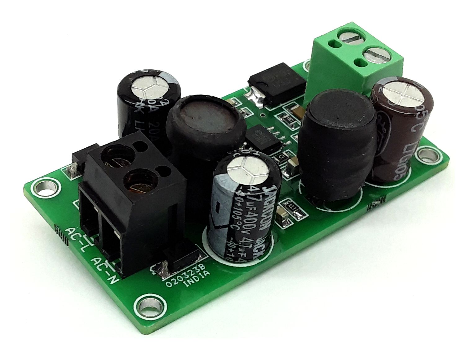
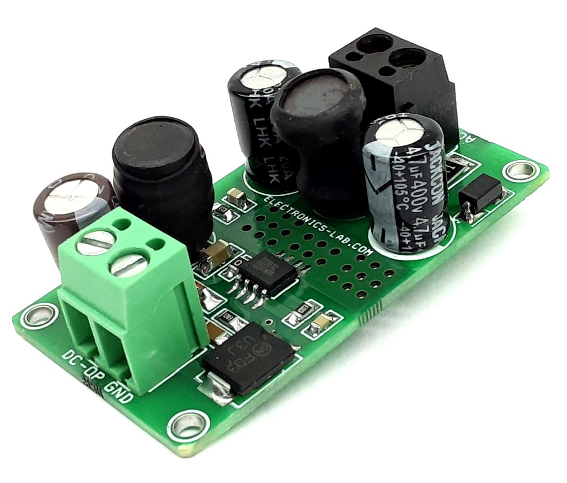
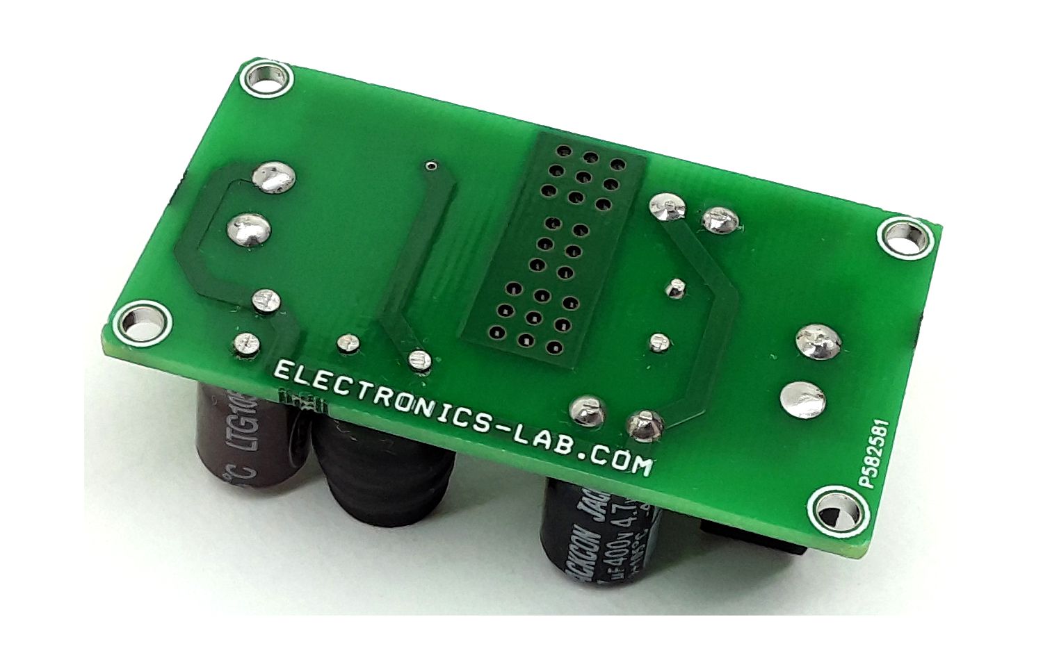
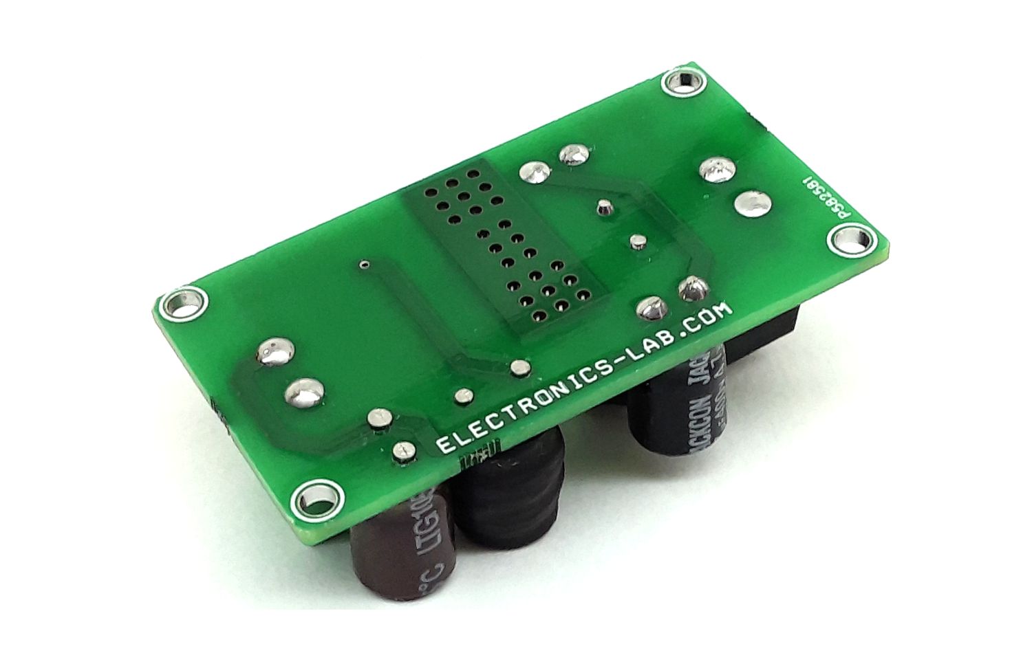
Photos


 With a strong