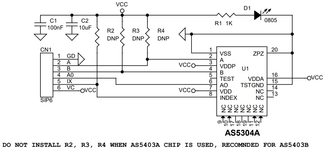
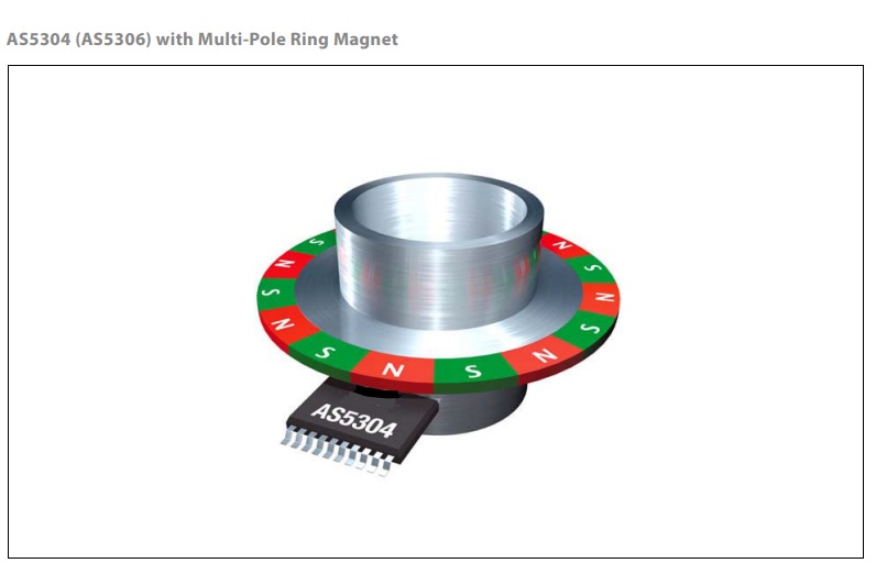
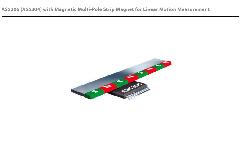
This sensor module is a simple solution to build a magnet-based rotary encoder. The project is based on the AS5304 chip with integrated Hall elements for measuring linear or rotary motion using multi-pole magnetic strips or rings. This allows the usage of the module in applications where the Sensor IC cannot be mounted at the end of a rotating device (e.g. at hollow shafts). Instead, the module is mounted off-axis underneath a multi-pole magnetized ring or strip and provides a quadrature incremental output with 40 pulses per pole period at speeds of up to 20 meters/second. A single index pulse is generated once for every pole pair at the Index output. Using, for example, a 32-pole-pair magnetic ring, the module can provide a resolution of 1280 pulses/revolution, which is equivalent to 5120 positions/revolution or 12.3bit. The maximum speed at this configuration is 9375 rpm. Recommended pole pair length is 4mm (2mm north pole / 2mm south pole). The chip accepts a magnetic field strength down to 5mT (peak).
Features
- 5V to 5.5V operating voltage
- Current Consumption 30 to 40mA
- High speed, up to 20m/s
- Magnetic pole pair length: 4mm
- Resolution of 1280 Pulses/Revolution
- Resolution: 25μm
- 40 pulses / 160 positions per magnetic period
- Quadrature Output Index, Channel A and Channel B with Pullups
- AO – AGC Analog Output. (Used to detect low magnetic field strength)
- 1 index pulse per pole pair
- Linear movement measurement using multi-pole magnetic strips
- Circular off-axis movement measurement using multi-pole magnetic rings
- Magnetic field strength indicator, magnetic field alarm for end-of-strip or missing magnet
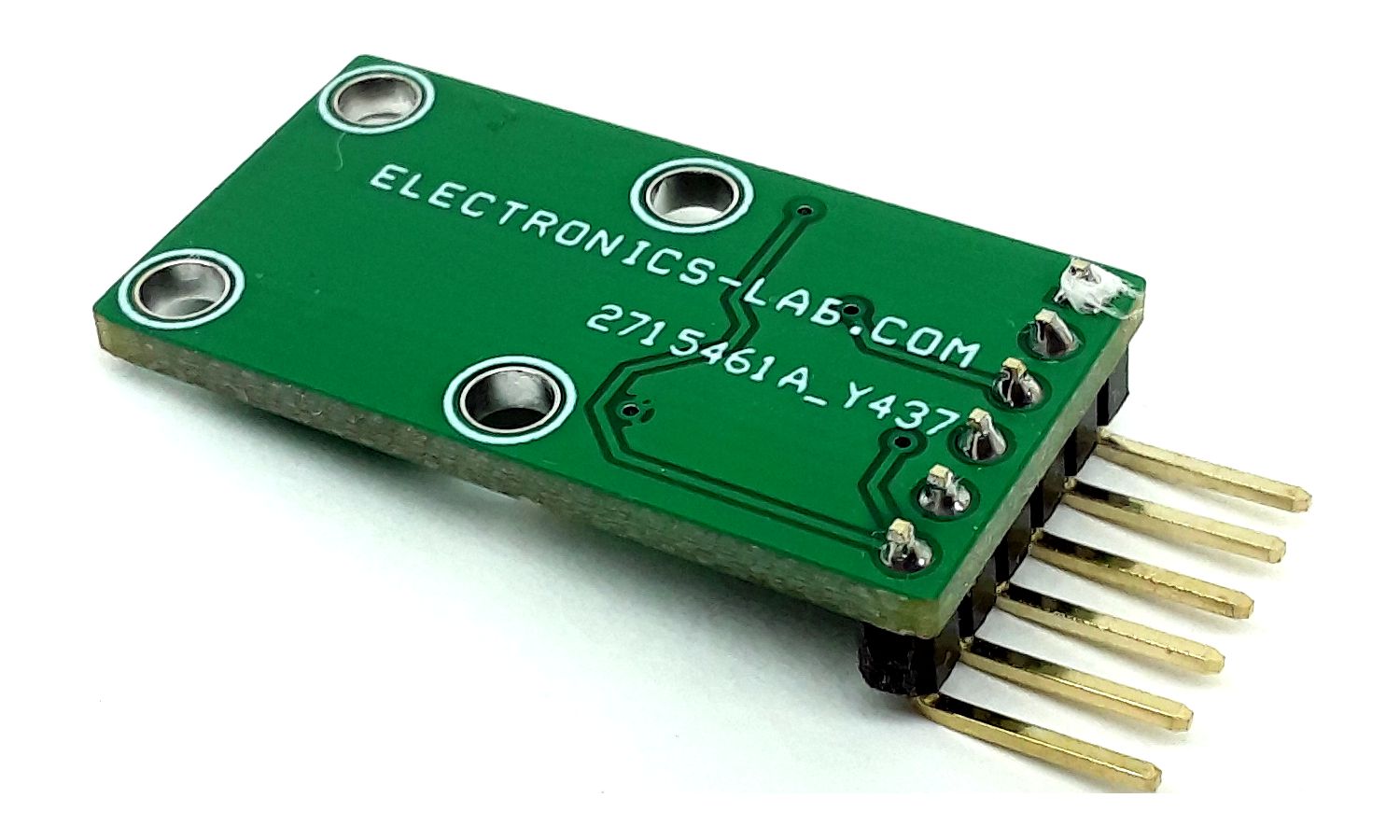
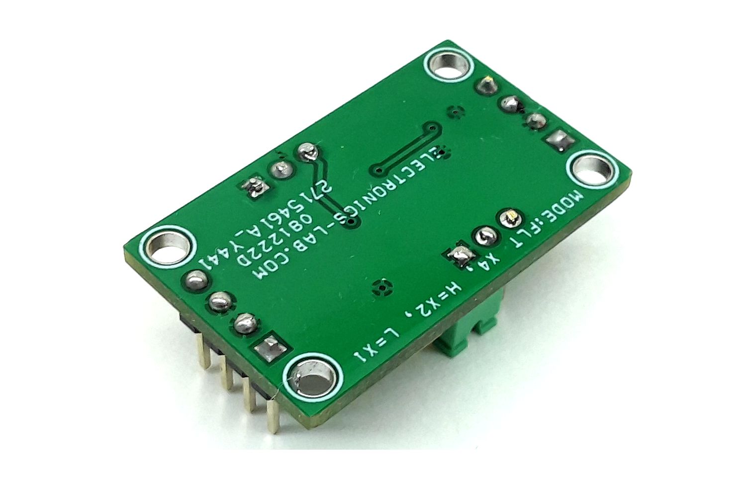
- PCB Dimensions 29.21 x 15.88mm
- 4 x 2.5mm Mounting Holes
Benefits and Key Features
- Contactless motion and position sensing
- High-speed measurement
- Robust against external magnetic stray fields
- Highest reliability and durability in harsh environments
- Control of high-speed movements
- Lower material cost (no magnetic shielding needed)
Magnet
- Magnetic pole length 2mm
- Magnetic pole pair length 4mm
- Magnetic amplitude 10-60mT
- Magnetic offset +/-0.5mT
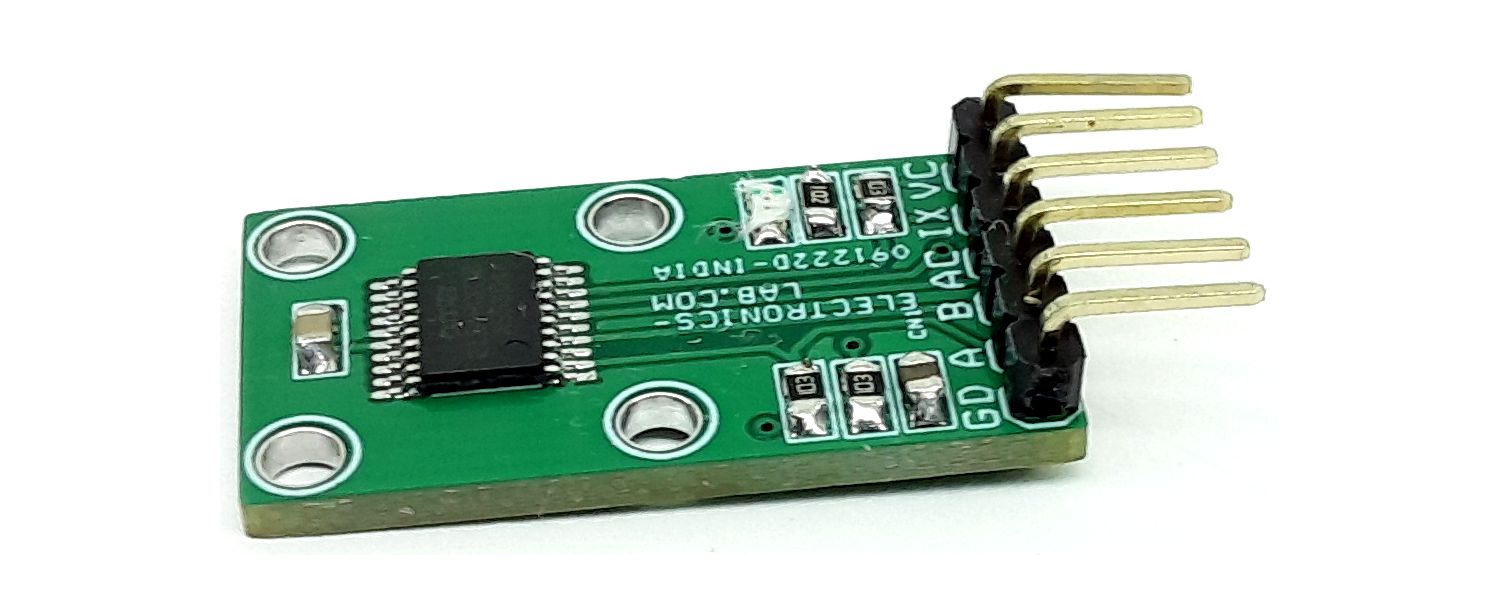
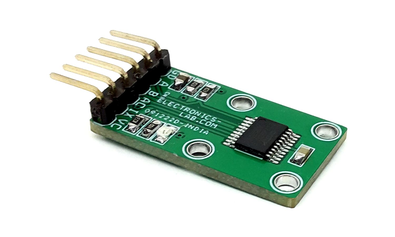
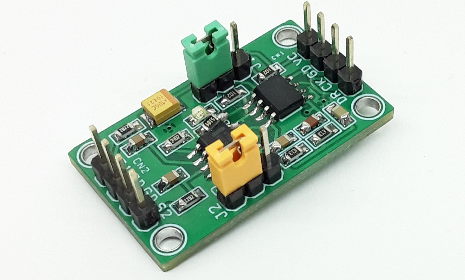
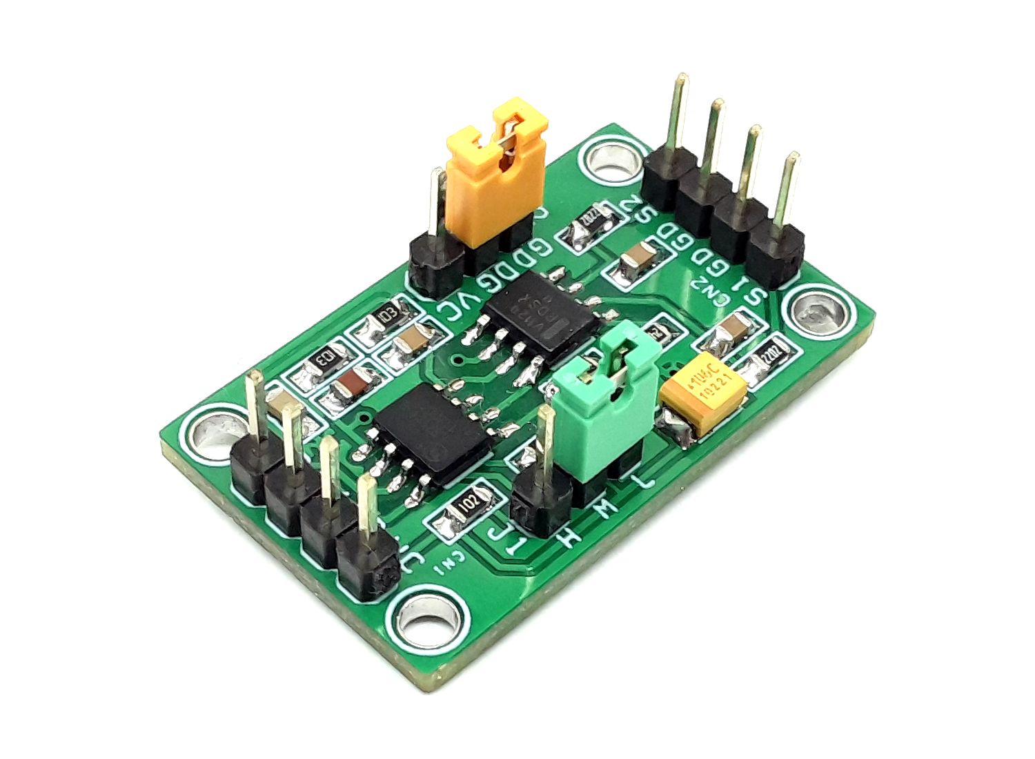
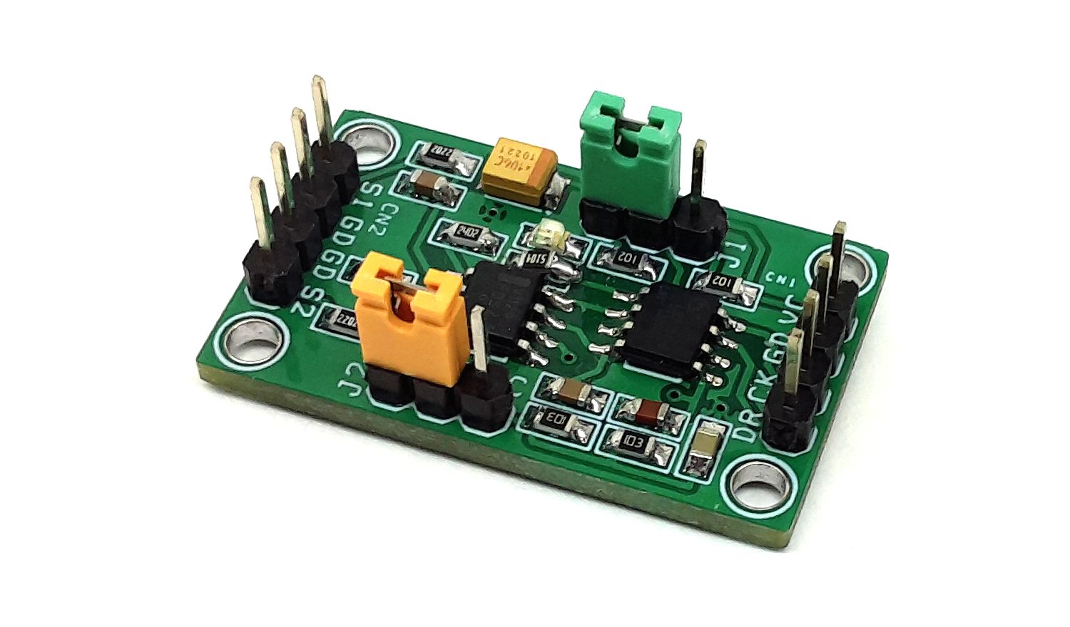
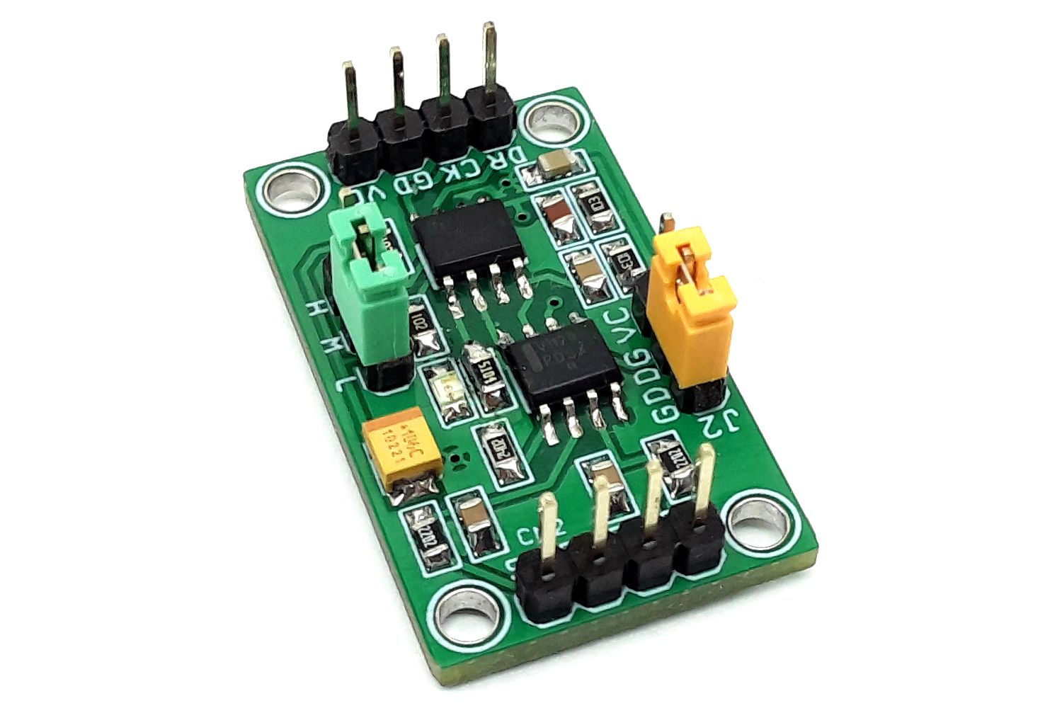
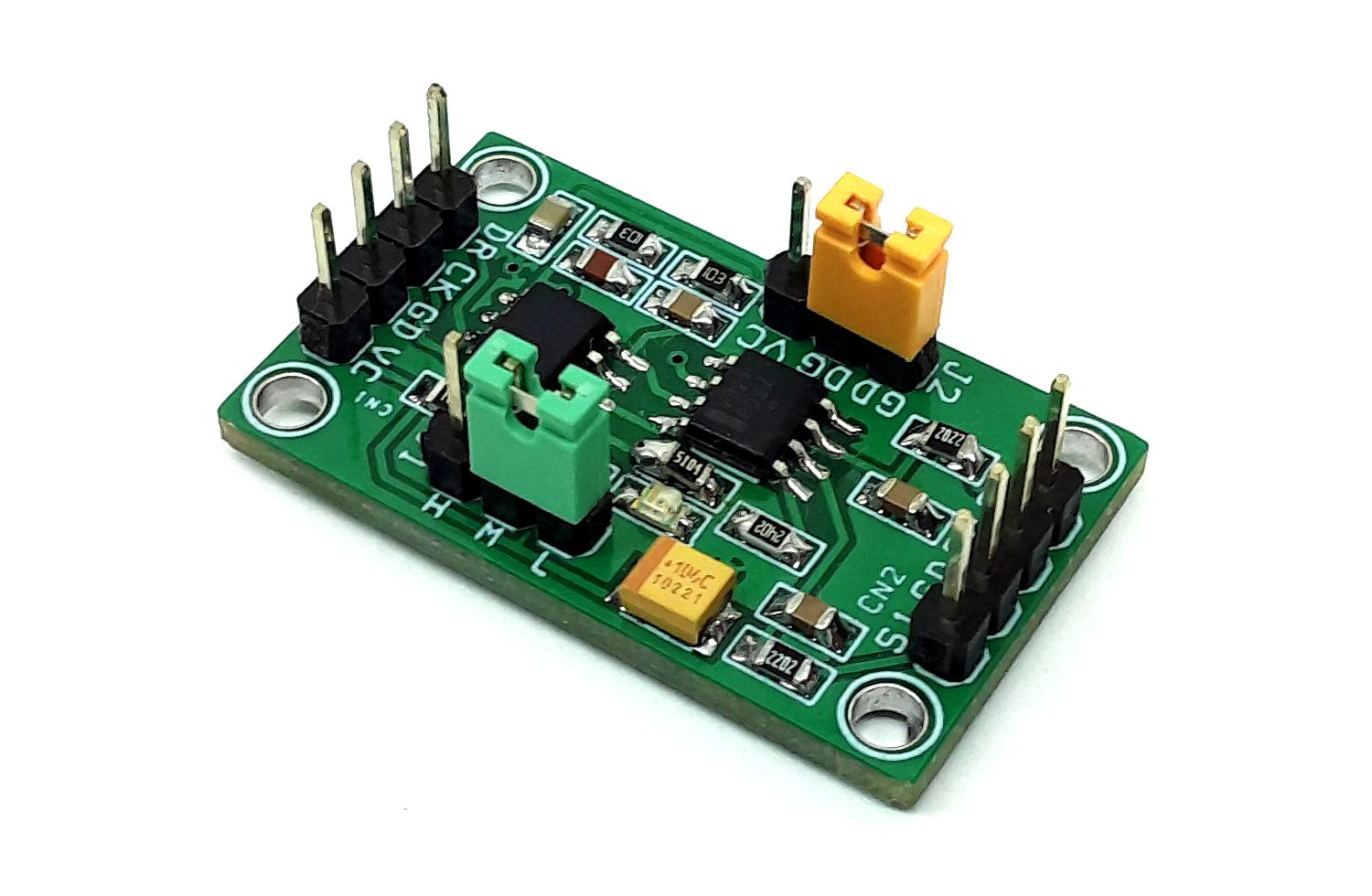
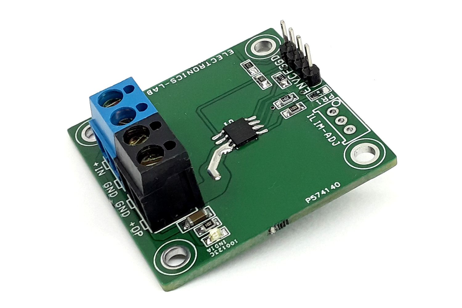
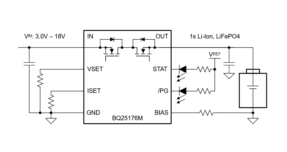
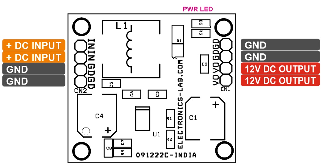
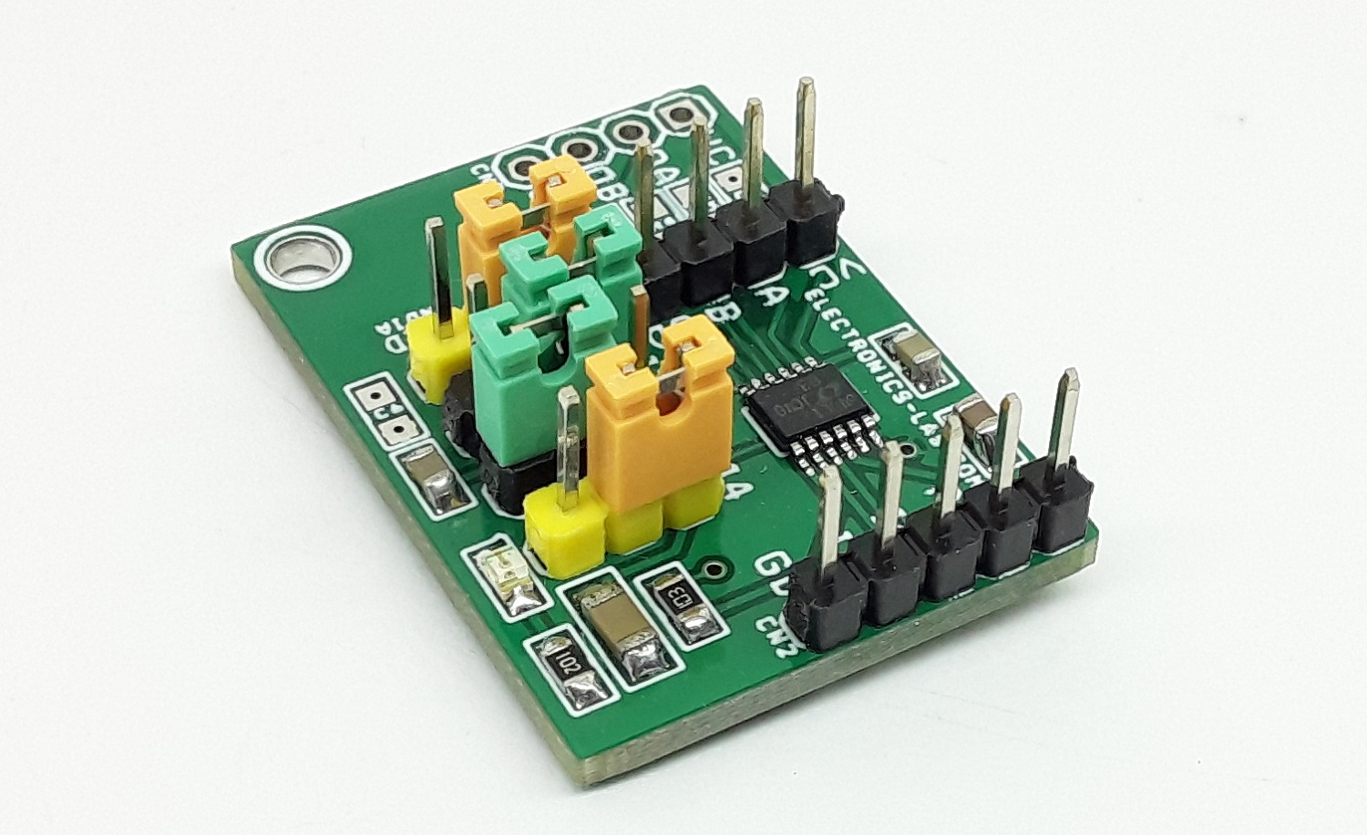
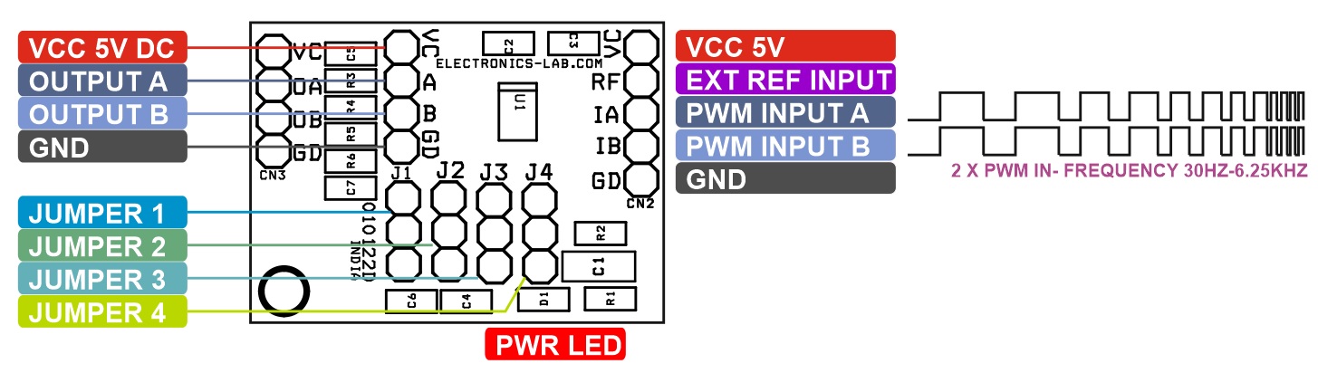
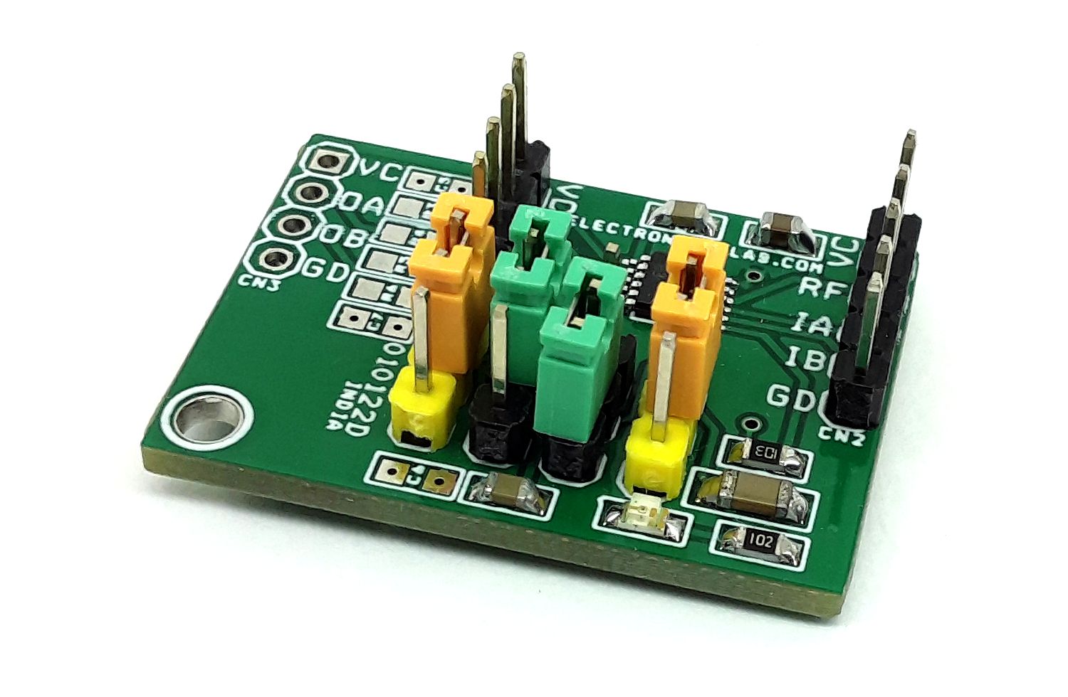
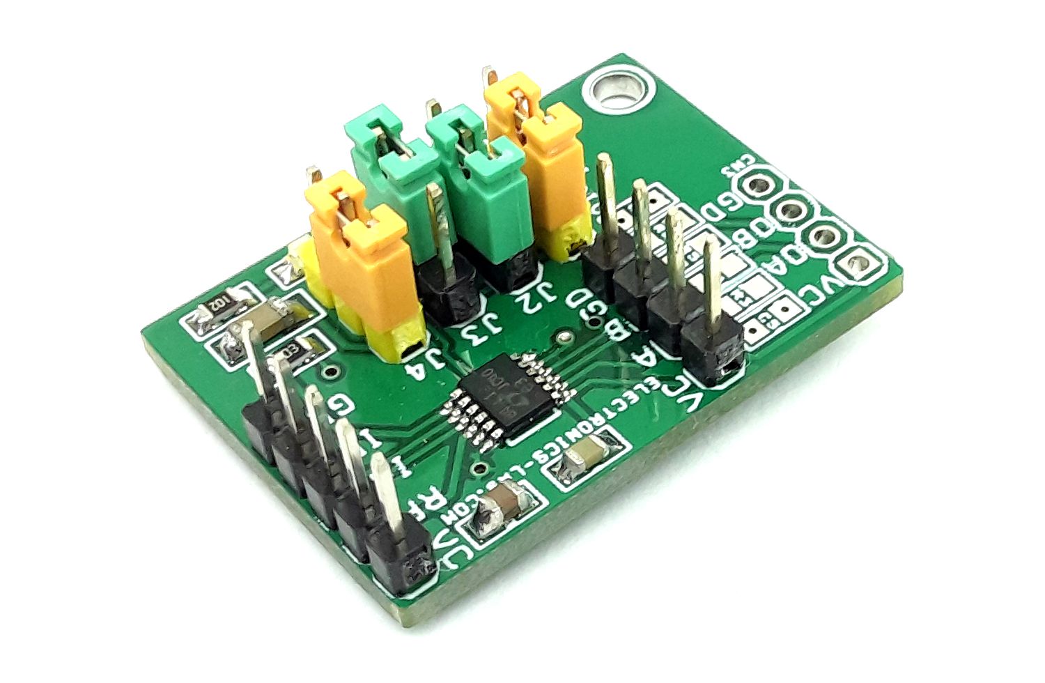
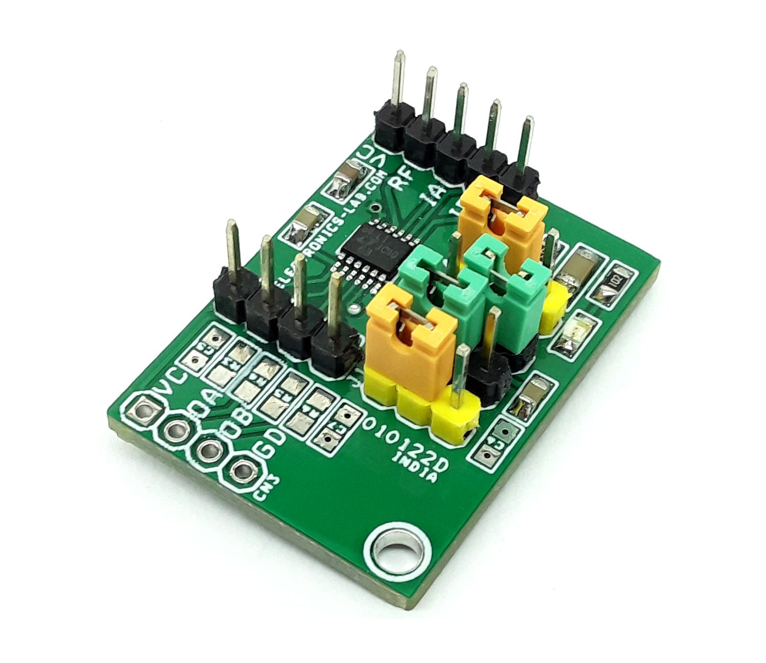
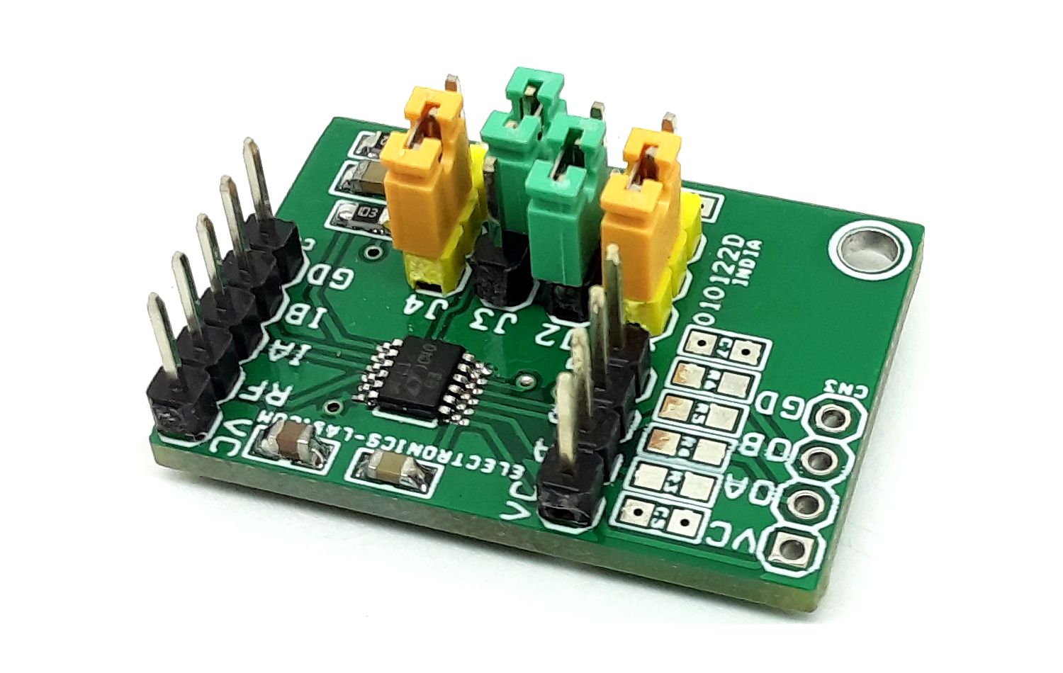
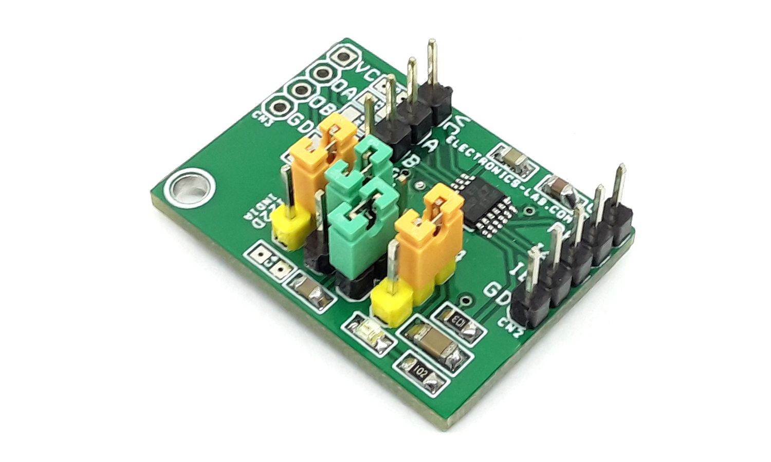
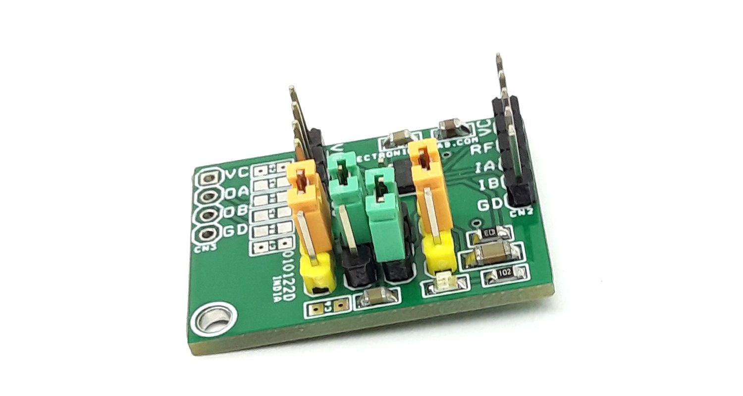
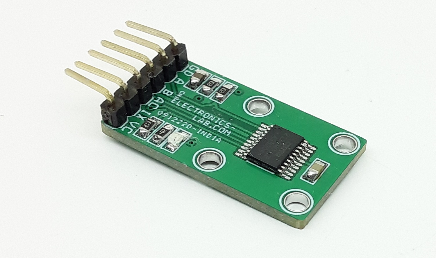
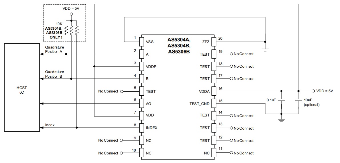
Connections and Other Details
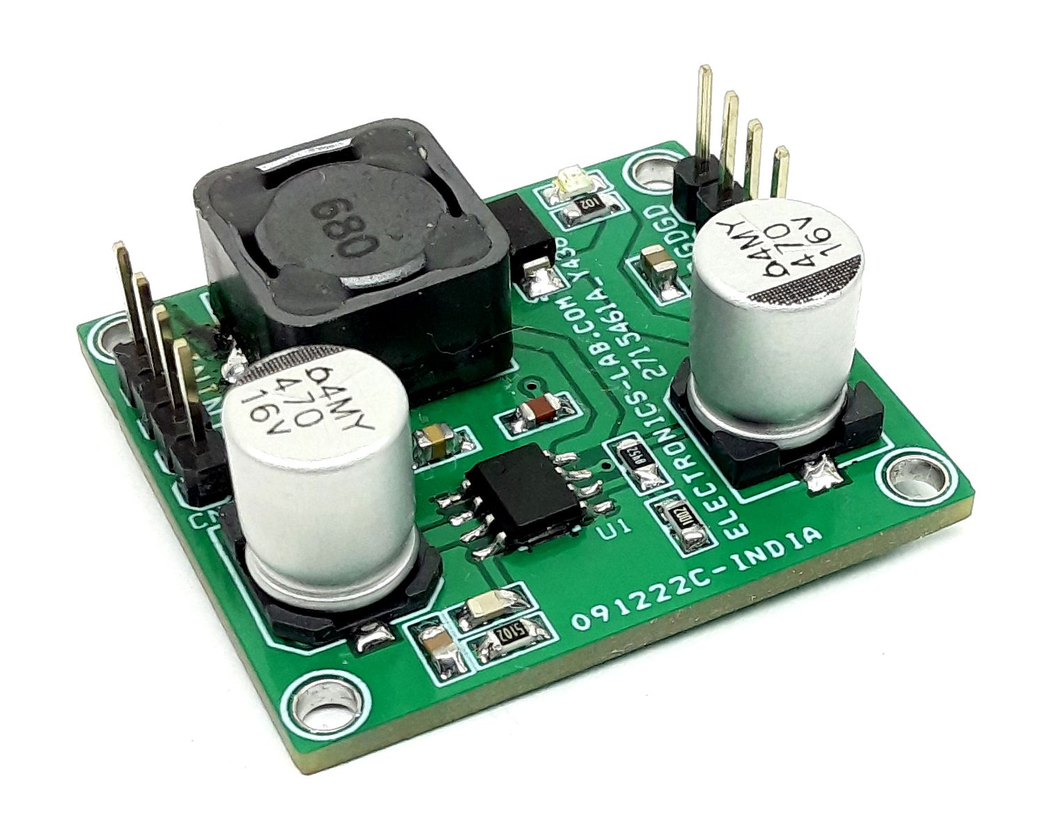
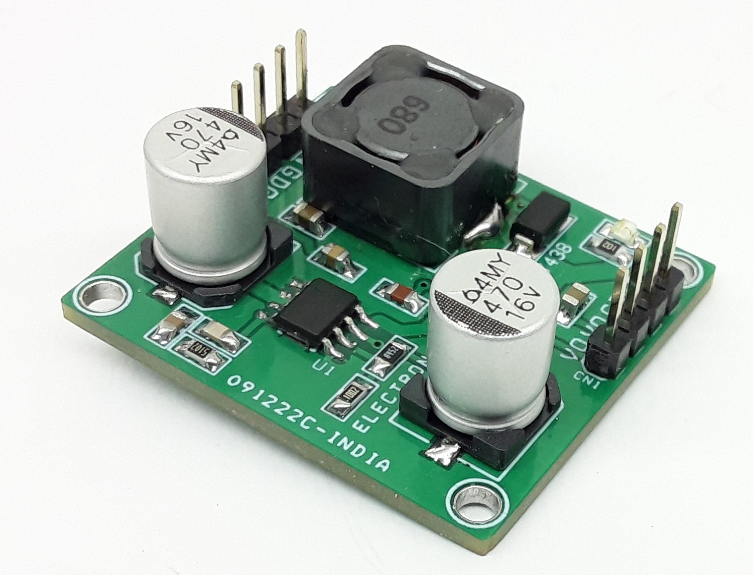
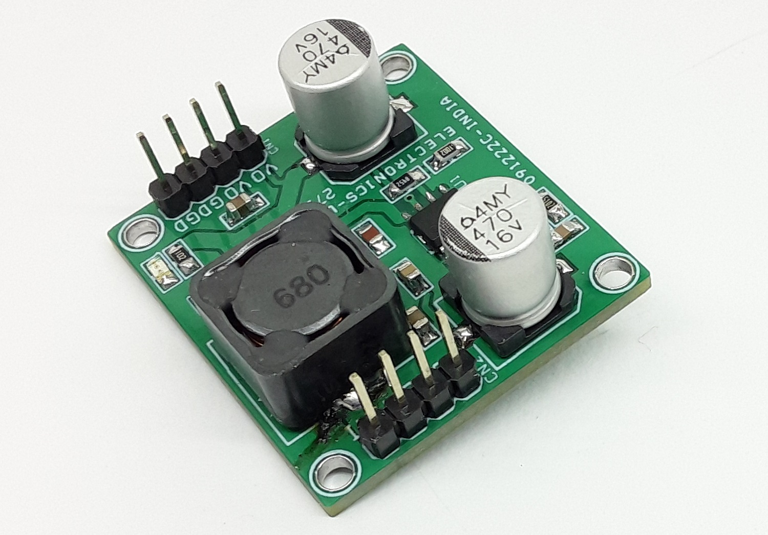
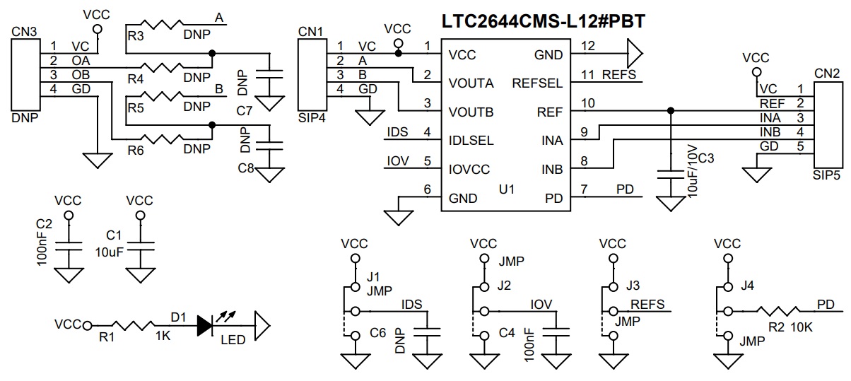
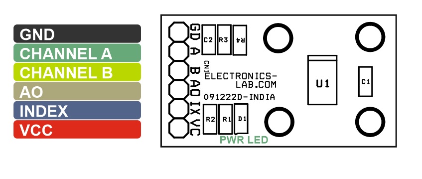
- CN1: Pin 1 = GND, Pin 2 = Channel A Out, Pin 3 = Channel B Out, Pin 4 = AO Out, Pin 5 = Index Out, Pin 6 = VCC
- D1: Power LED
Outputs
- Incremental quadrature position output A. Short circuit current limitation
- Incremental quadrature position output B. Short Circuit Current Limitation
- Index output, active HIGH. Short Circuit Current Limitation
- AGC Analog Output. (Used to detect low magnetic field strength)
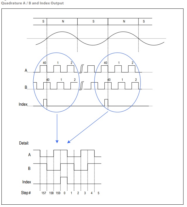
Incremental Quadrature AB Output
The digital output is compatible with optical incremental encoder outputs. The direction of rotation is encoded into two signals A and B that are phase-shifted by 90º. Depending on the direction of rotation, A leads B (CW) or B leads A (CCW).
Index Pulse
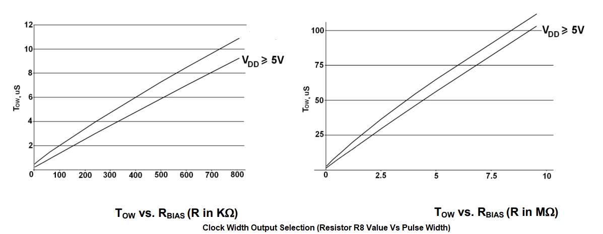
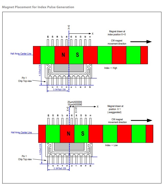
A single index pulse is generated once for every pole pair. One pole pair is interpolated to 40 quadrature pulses (160 steps), so one index pulse is generated after every 40 quadrature pulses. The Index output is switched to Index = high, when a magnet is placed over the Hall array, the north pole of the magnet is placed over the left side of the IC (top view, pin#1 at bottom left) and the south pole is placed over the right side of the IC. The index output will switch back to Index = low, when the magnet is moved by one LSB from position X=0 to X=X1. One LSB is 25μm.
The AO Output
The Analog Output (AO) provides an analog output voltage representing the Automatic Gain Control (AGC) of the Hall sensors signal control loop. This voltage can be used to monitor the magnetic field strength and hence the gap between the magnet and chip surface:
- Short distance between magnet and IC -> strong magnetic field -> low loop gain -> low AO voltage
- Long distance between magnet and IC -> weak magnetic field -> high loop gain -> high AO voltage
Magnetic Field Warning Indicator
The Module can also provide a low magnetic field warning to indicate a missing magnet or when the end of the magnetic strip has been reached. This condition is indicated by using a combination of A, B and Index, which does not occur in normal operation: A low magnetic field is indicated with: Index = high A=B=low
Vertical Distance between Magnet and IC
The recommended vertical distance between the magnet and IC depends on the strength of the magnet and the length of the magnetic pole. Typically, the vertical distance between magnet and chip surface should not exceed ½ of the pole length. That means for the AS5304 module, having a pole length of 2.0mm, the maximum vertical gap should be 1.0mm. These figures refer to the chip surface. Given a typical distance of 0.2mm between chip surface and IC package surface, the recommended vertical distances between the magnet and IC surface are therefore: AS 5304: ≤ 0.8mm
Soft Stop Feature for Linear Movement Measurement
When using long multi-pole strips, it may often be necessary to start from a defined home (or zero) position and obtain absolute position information by counting the steps from the defined home position. The AS5304 module provides a soft stop feature that eliminates the need for a separate electro-mechanical home position switch or an optical light barrier switch to indicate the home position. The magnetic field warning indicator (see Magnetic Field Warning Indicator- refer datasheet of chip) together with the index pulse can be used to indicate a unique home position on a magnetic strip:
- Firstly, the AS5304 module moves to the end of the strip until a magnetic field warning is displayed (Index = high, A=B=low).
- Then, the AS5304 module moves back towards the strip until the first index position is reached (Note that an index position is generated once for every pole pair, it is indicated with: Index = high, A=B= high). Depending on the polarity of the strip magnet, the first index position may be generated when the end of the magnet strip only covers one-half of the Hall array. This position is not recommended as a defined home position, as the accuracy of the AS5304 module are reduced as long as the multi-pole strip does not fully cover the Hall array. 3. It is therefore recommended to continue to the next (second) index position from the end of the strip (Index = high, A=B= high). This position can now be used as a defined home position.
Incremental Hysteresis
If the magnet is sitting right at the transition point between two steps, the noise in the system may cause the incremental outputs to jitter back and forth between these two steps, especially when the magnetic field is weak. To avoid this unwanted jitter, a hysteresis has been implemented.
Resolution and Maximum Rotating Speed
When using the AS5304A module in an off-axis rotary application, a multi-pole ring magnet must be used. Resolution, diameter and maximum speed depend on the number of pole pairs on the ring.
Resolution
The angular resolution increases linearly with the number of pole pairs. One pole pair has a resolution (= interpolation factor) of 160 steps or 40 quadrature pulses.
Resolution [steps] = [interpolation factor] x [number of pole pairs] Resolution [bit] = log (resolution[steps]) / log (2) Example: Multi-pole ring with 22 pole pairs Resolution = 160×22 = 3520 steps per revolution = 40×22 = 880 quadrature pulses / revolution = 11.78 bits per revolution = 0.1023° per step
Multi-Pole Ring Diameter
The length of a pole pair across the median of the multi-pole ring must remain fixed at either 4mm. Hence, with increasing pole pair count, the diameter increases linearly with the number of pole pairs on the magnetic ring.
Magnetic ring diameter = [pole length] * [number of pole pairs] / π for AS5304 module: d = 4.0mm * number of pole pairs / π
Example: (same as above) multi-pole ring with 22 pole pairs for AS5304 Ring diameter = 4 * 22 / 3.14 = 28.01mm (this number represents the median diameter of the ring.
Maximum Rotation Speed
The AS5304 module uses a fast interpolation technique allowing an input frequency of 5kHz. This means it can process magnetic field changes in the order of 5000 pole pairs per second or 300000 revolutions per minute. However, since a magnetic ring consists of more than one pole pair, the above value must be divided by the number of pole pairs to get the maximum rotation speed: Maximum rotation speed = 300000 rpm / [number of pole pairs] Example: (same as above) multi-pole ring with 22 pole pairs: Maximum speed = 300000 / 22 = 13636 rpm (this is independent of the pole length)
Maximum Linear Travelling Speed
For linear motion sensing, a multi-pole strip using equally spaced north and south poles is used. The pole length is again fixed at 2.0mm for the module As shown in Maximum Rotation Speed above, the sensors can process up to 5000 pole pairs per second, so the maximum traveling speed is: Maximum linear travelling speed = 5000 * [pole pair length] Example: Linear multi-pole strip: Maximum linear travelling speed = 4mm * 5000 1/s = 20000mm/s = 20m/s {for AS5304 module}
Applications
The module is ideal for high-speed linear motion and off-axis rotation measurements in applications, such as electrical motors, X-Y-stages, rotation knobs, and industrial drives.
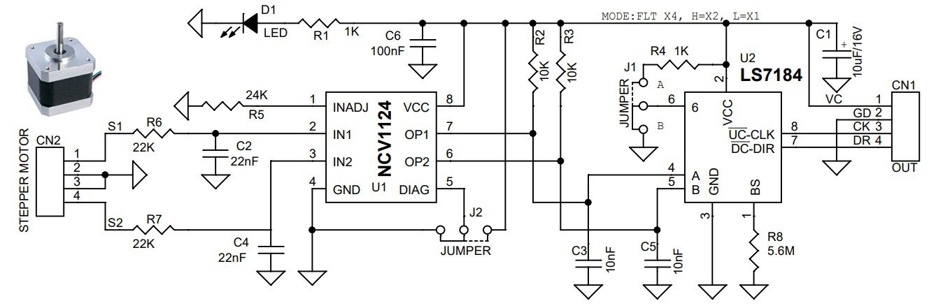
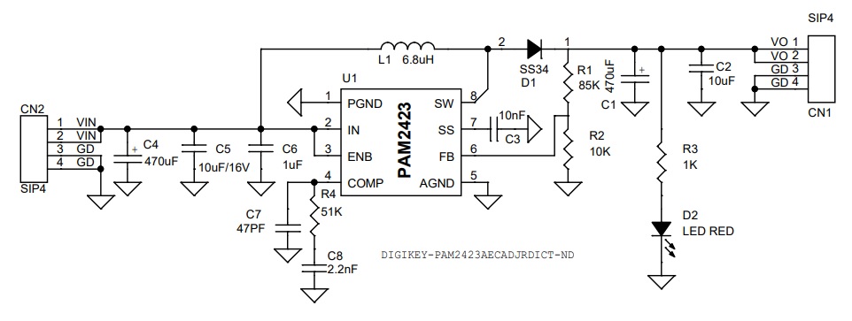
Schematic
Parts List
| NO. | QNTY. | REF. | DESC. | MANUFACTURER | SUPPLIER | SUPPLIER PART NO |
|---|---|---|---|---|---|---|
| 1 | 1 | CN1 | 6 PIN MALE HEADER 2.54MM | WURTH | DIGIKEY | 732-5319-ND |
| 2 | 1 | C1 | 100nF/25V CERAMIC SMD SIZE 0805 | MURATA/YAGEO | DIGIKEY | |
| 3 | 1 | C2 | 10uF/16V SMD SIZE 0805 | MURATA/YAGEO | DIGIKEY | |
| 4 | 1 | D1 | RED LED SMD SIZE 0805 | OSRAM | DIGIKEY | 475-1278-1-ND |
| 5 | 1 | R1 | 1K 5% SMD SIZE 0805 | MURATA/YAGEO | DIGIKEY | |
| 6 | 3 | R2,R3,R4 | DO NOT INSTALL | |||
| 7 | 1 | U1 | AS5304A OR AS5306B | ASM/OSRAM | DIGIKEY | AS5304A-ATSMCT-ND |
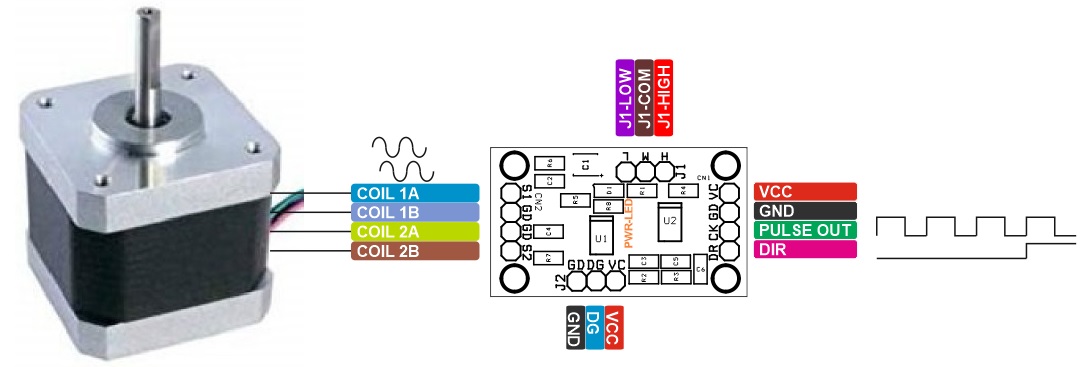
Connections
Application Schematic
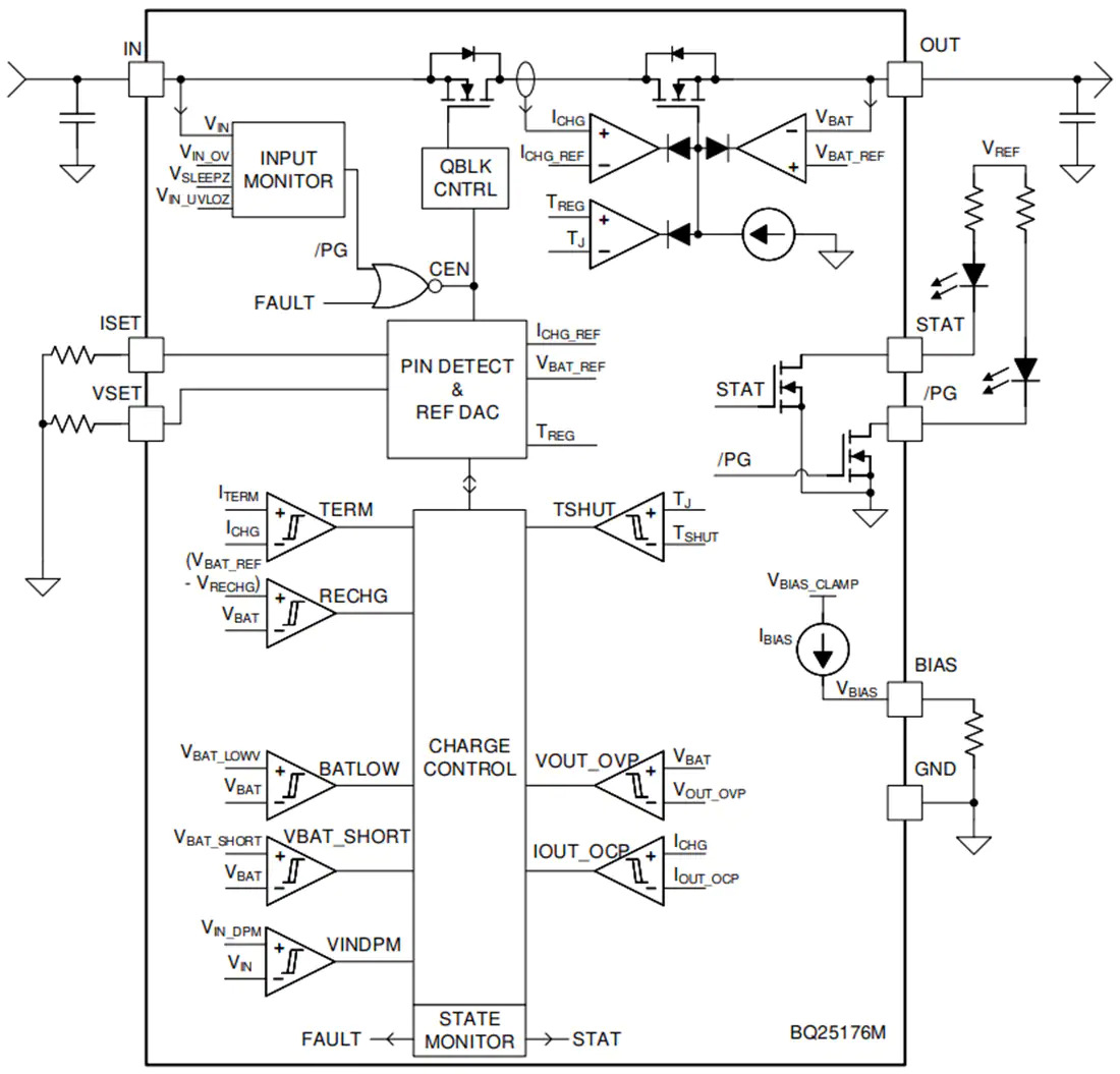
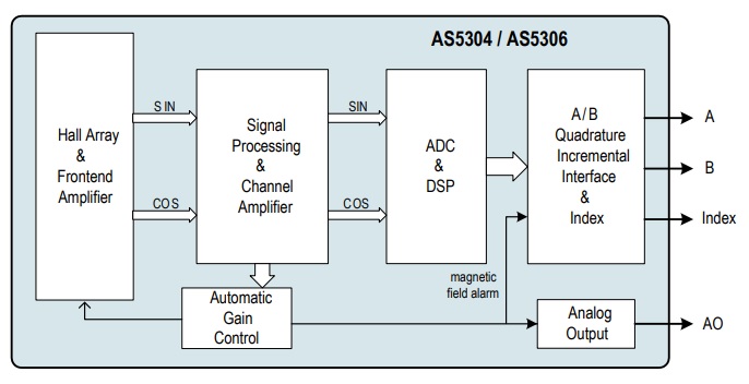
Internal Block Diagram
Magnet Placement
Output waveforms
Gerber View
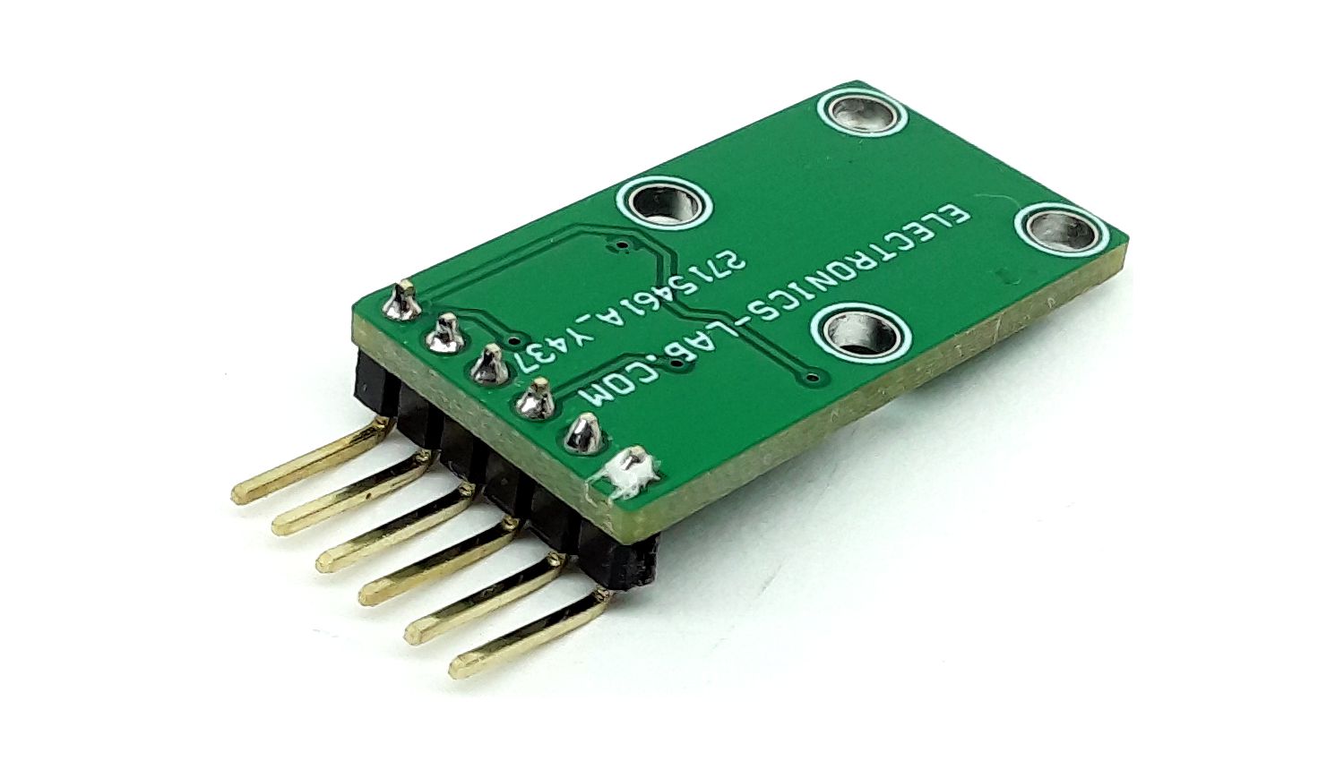
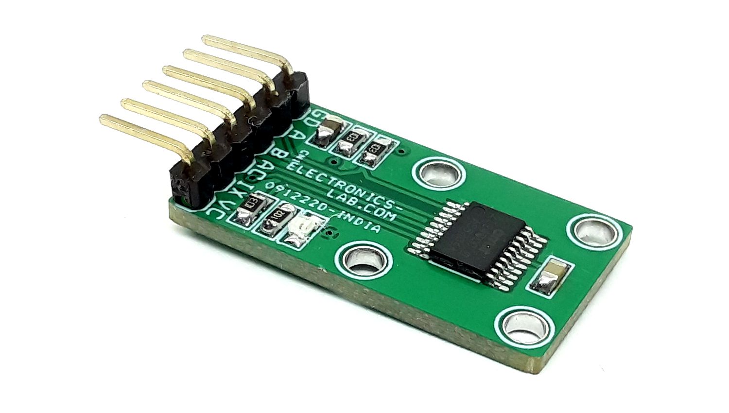
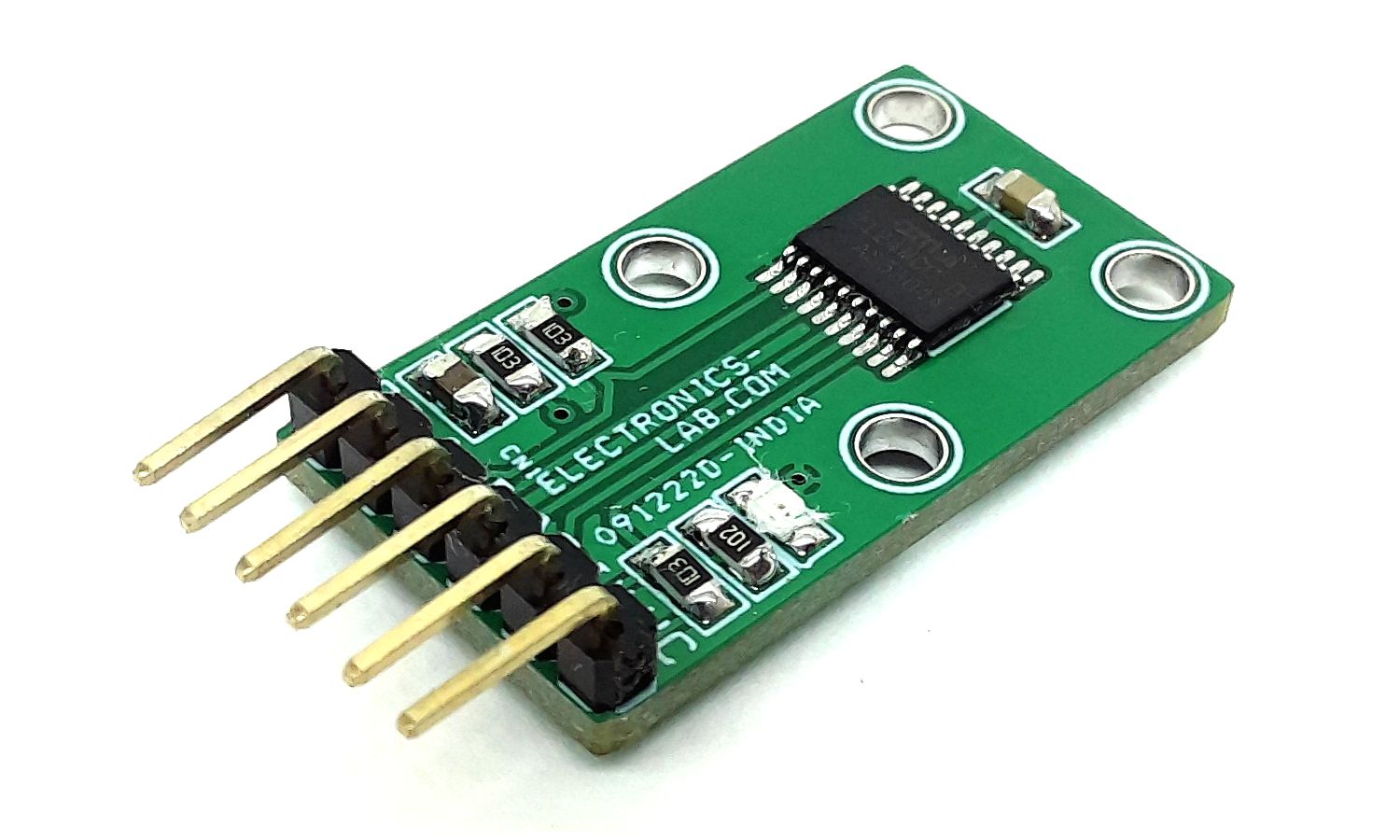
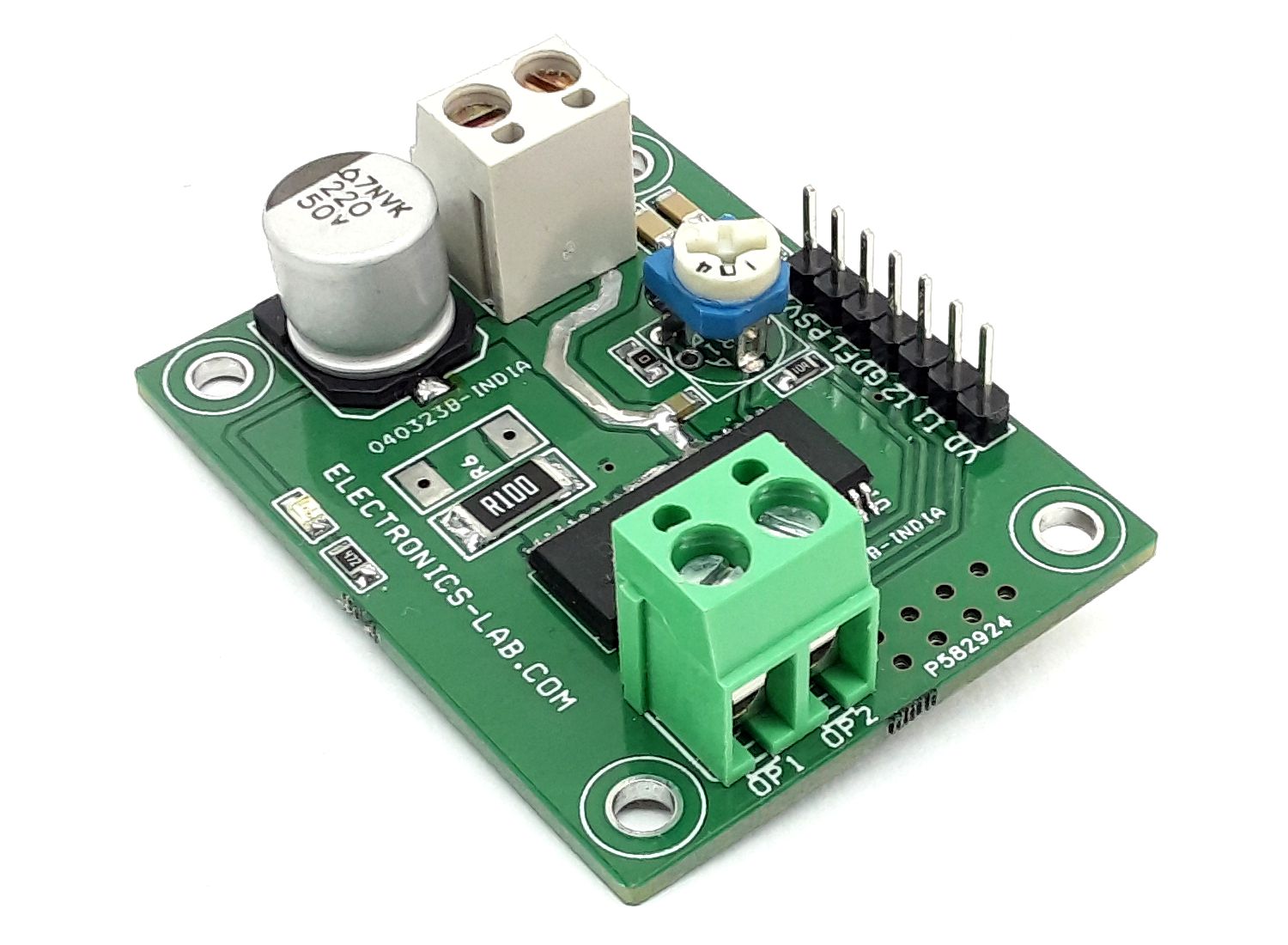
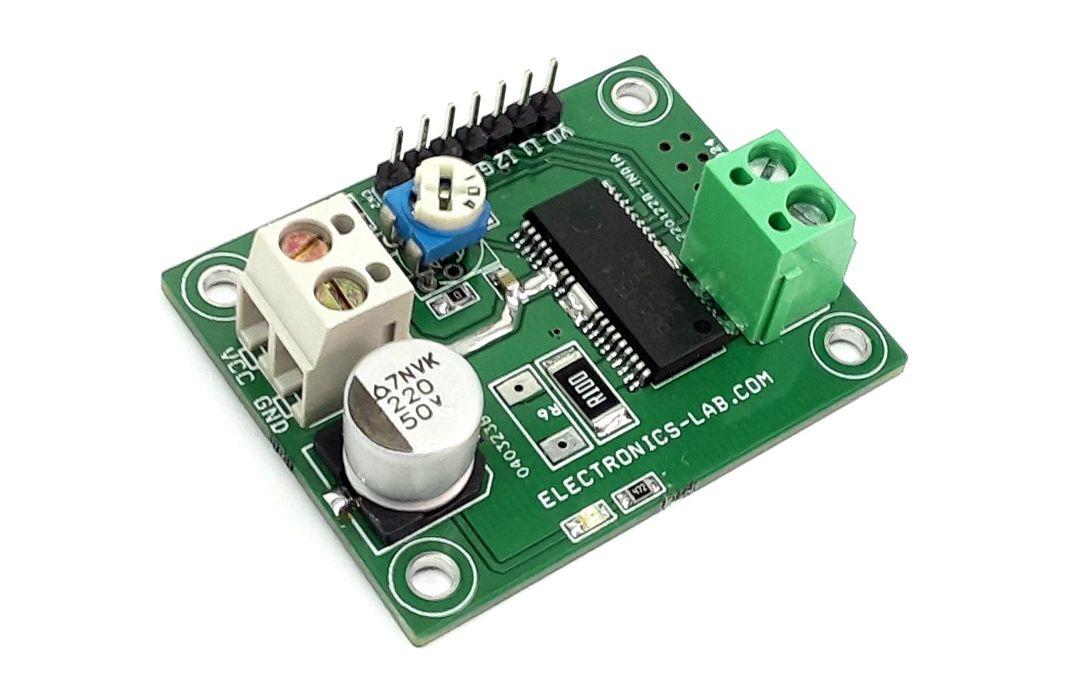
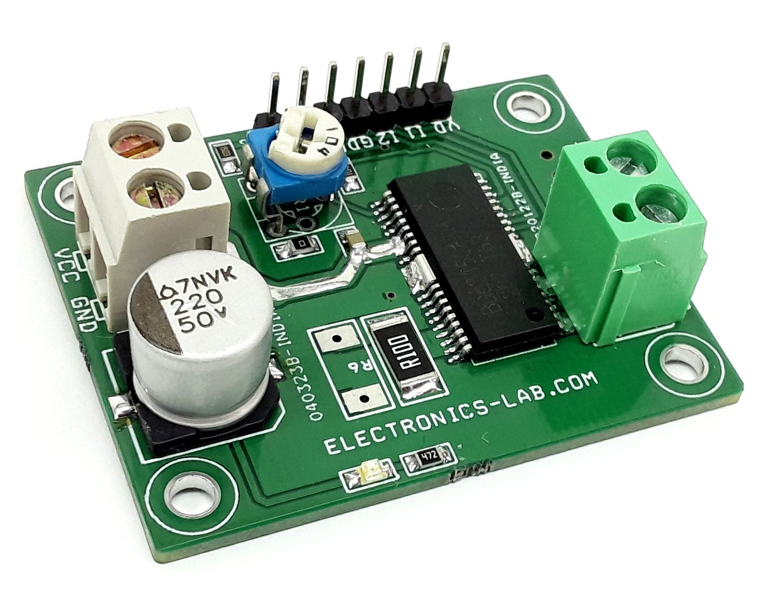
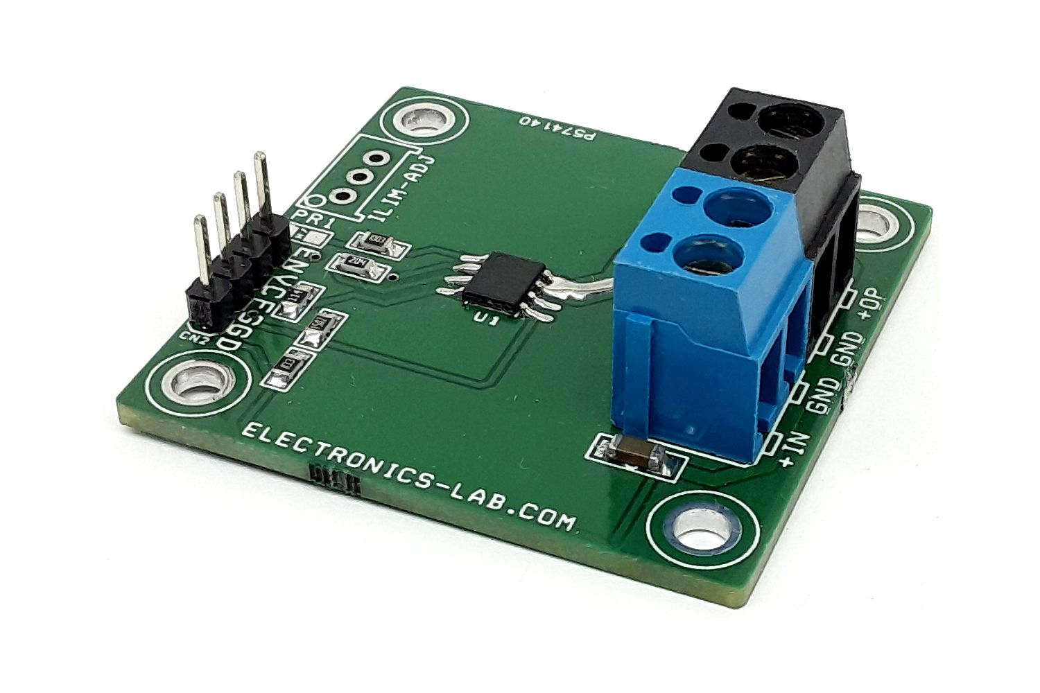
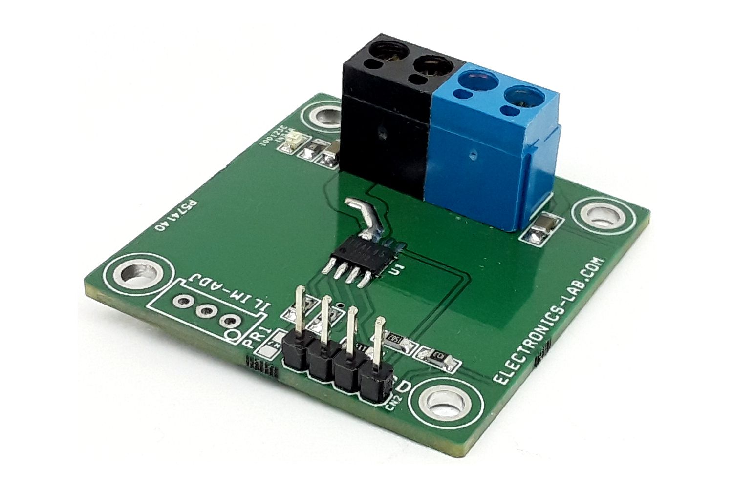
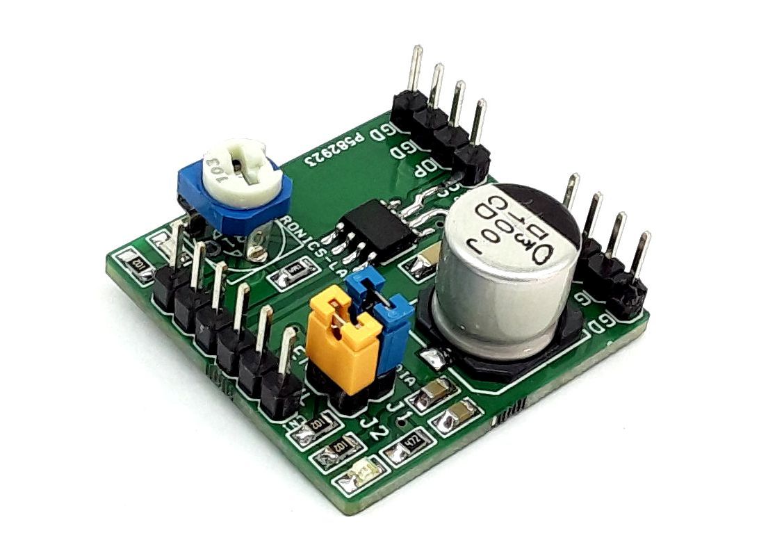
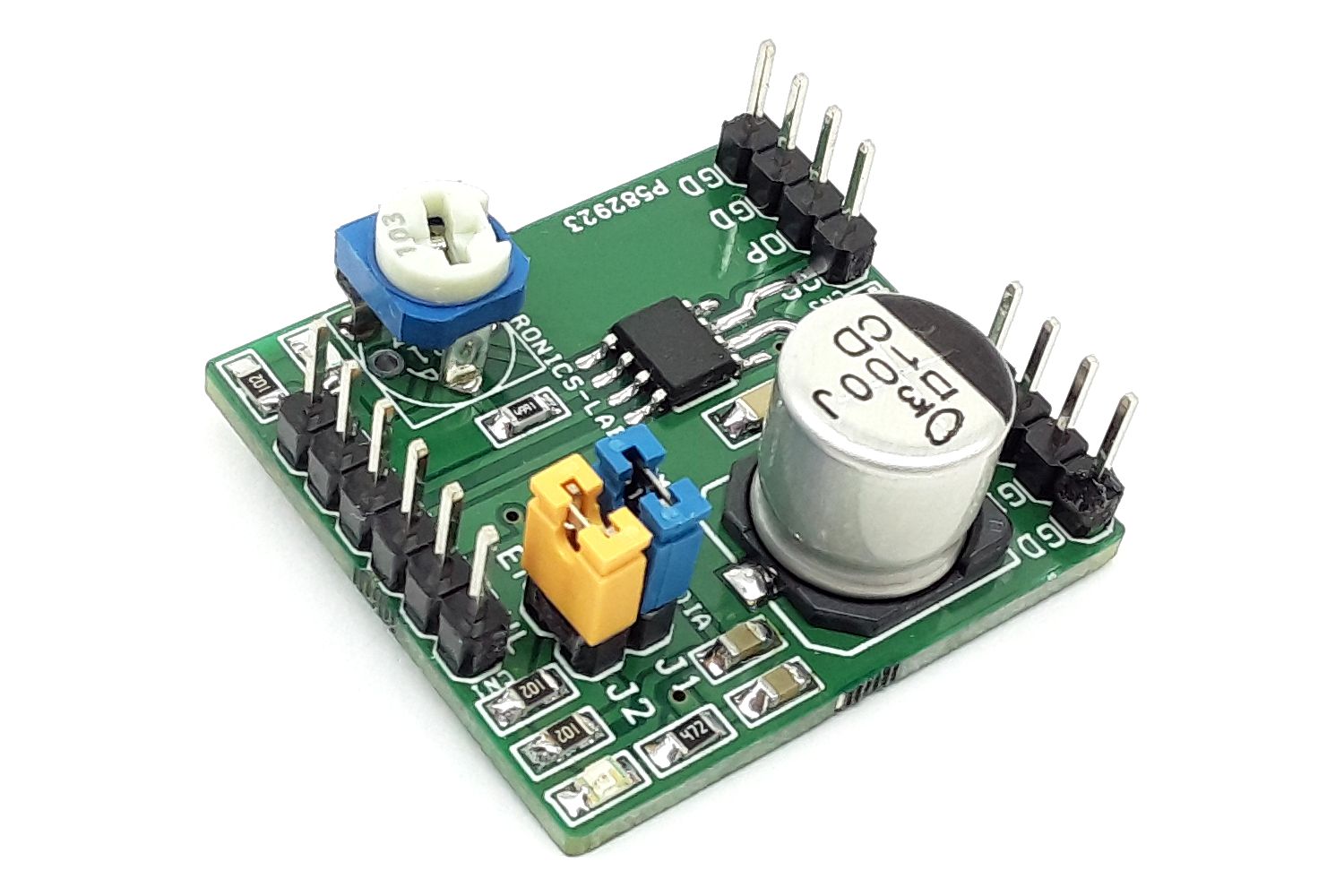
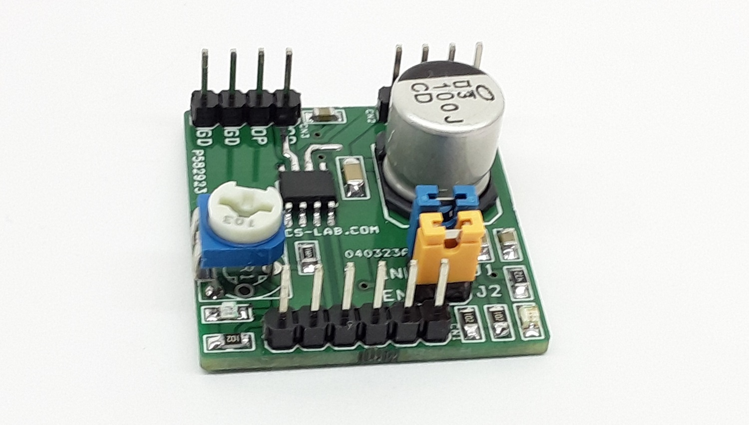
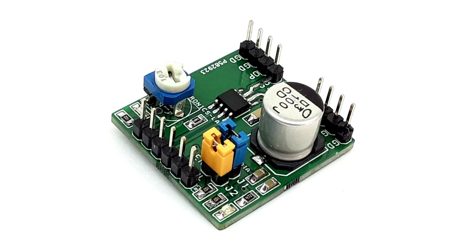
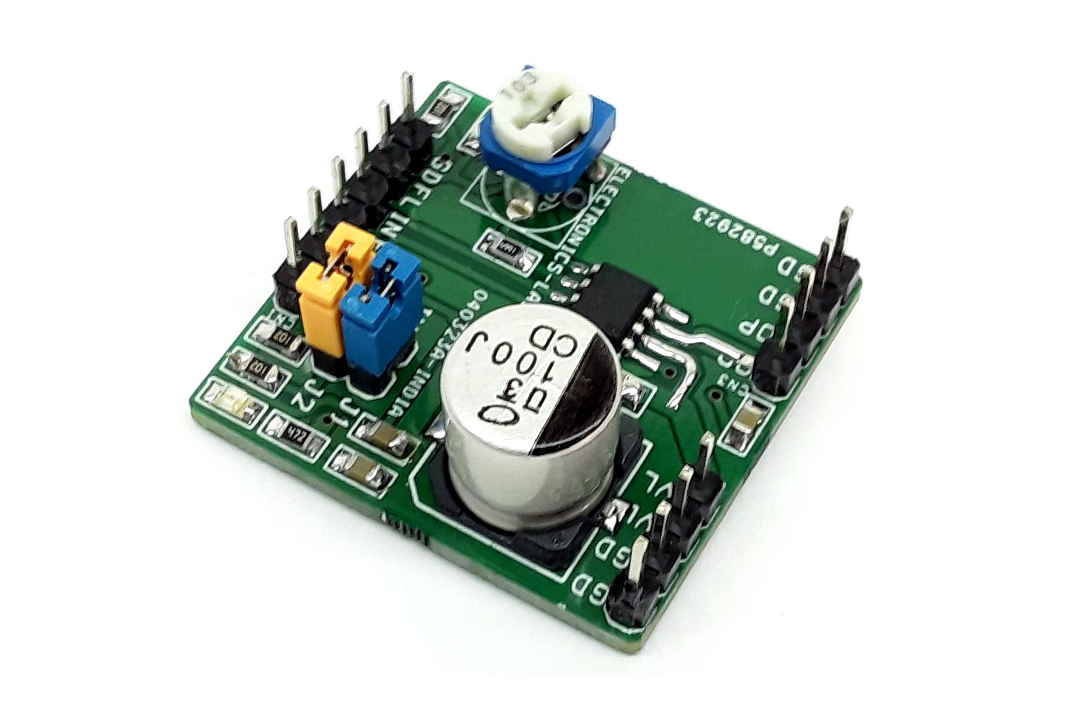
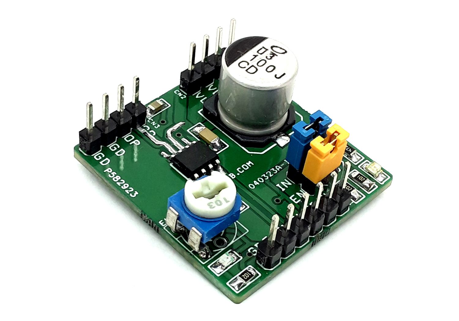
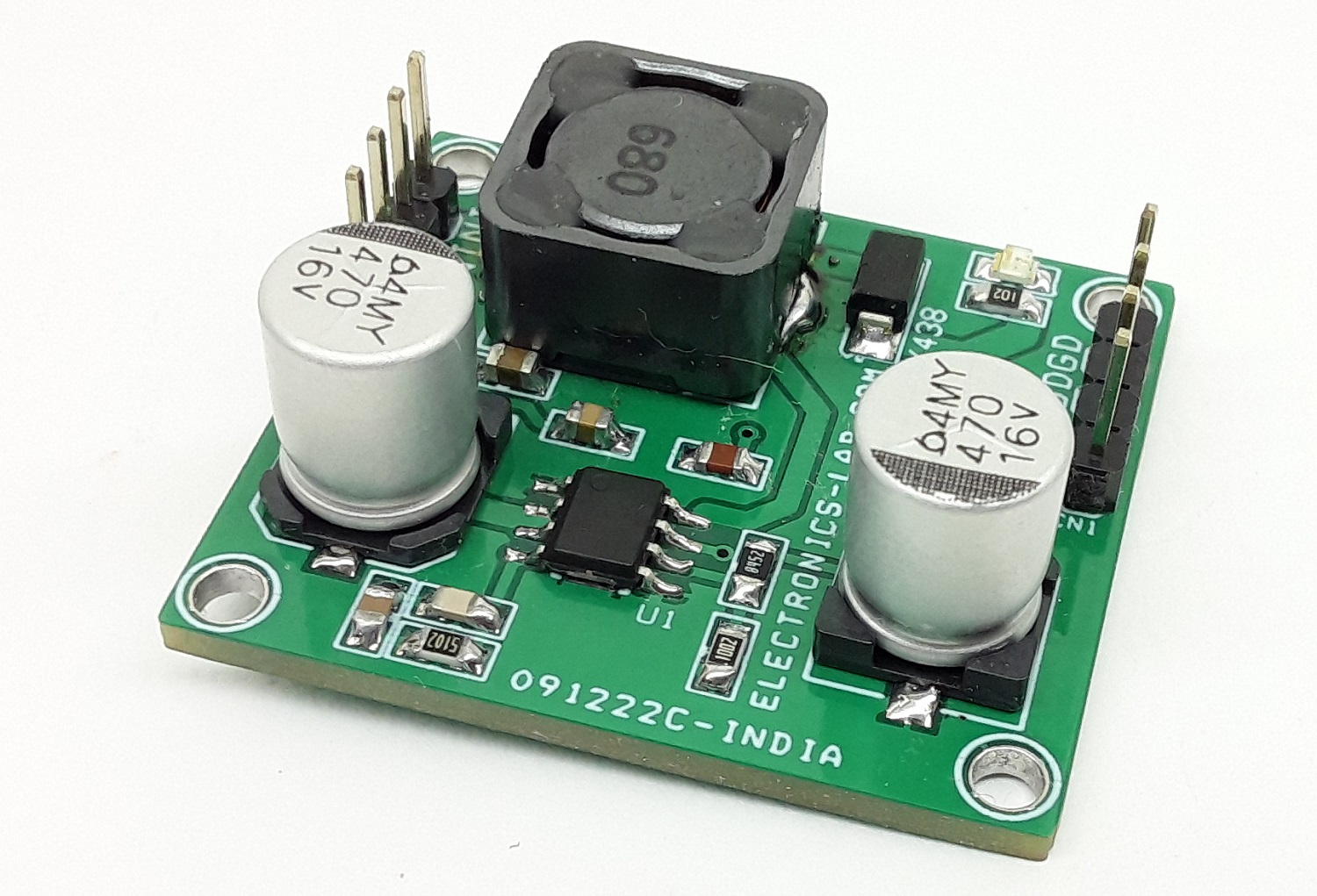
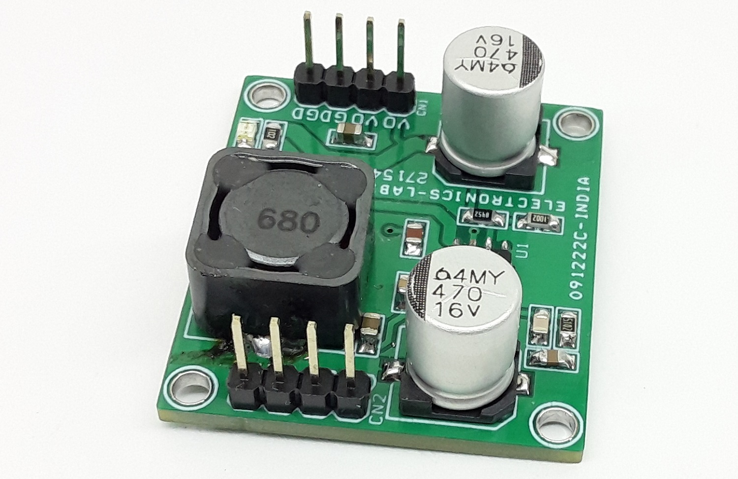
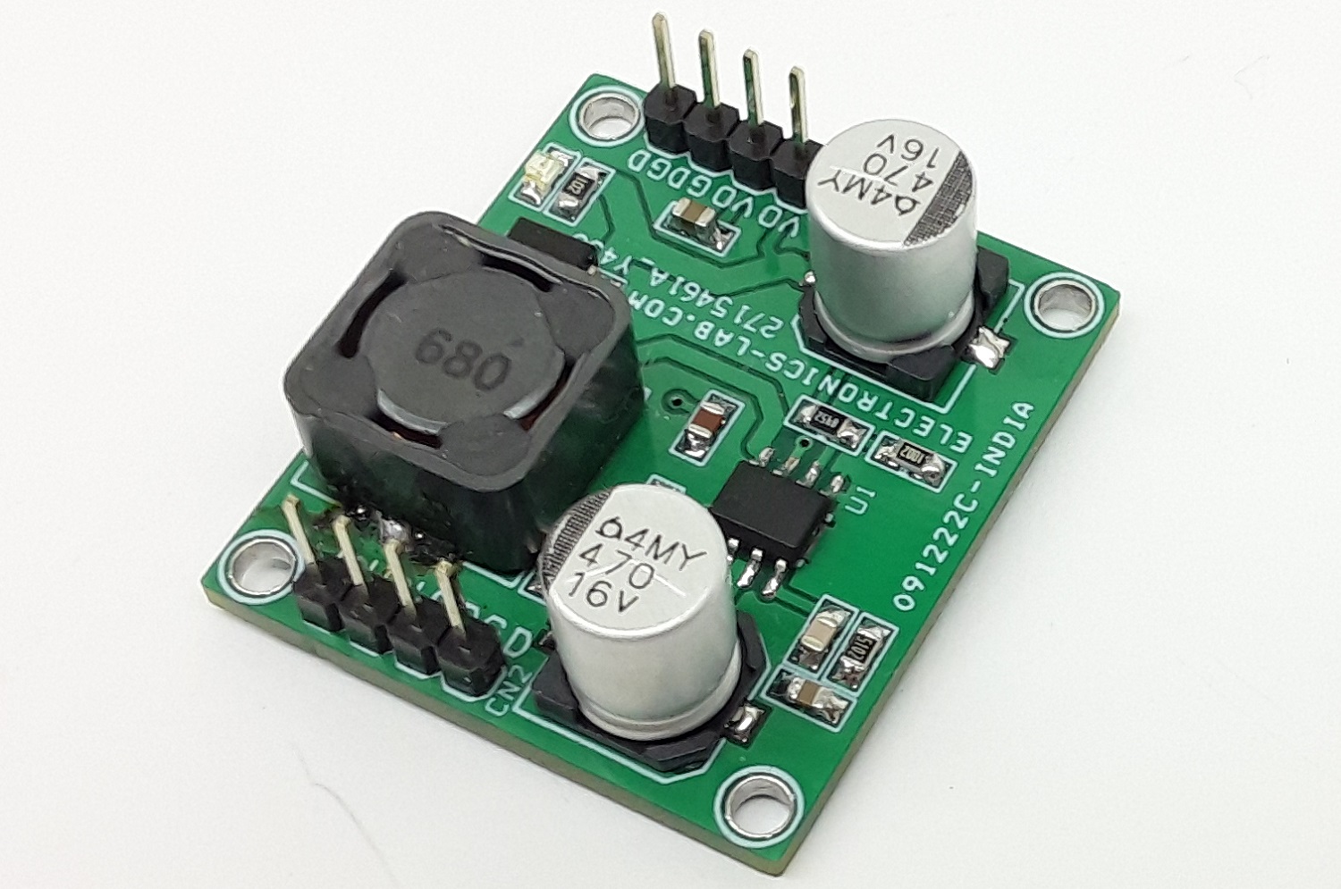
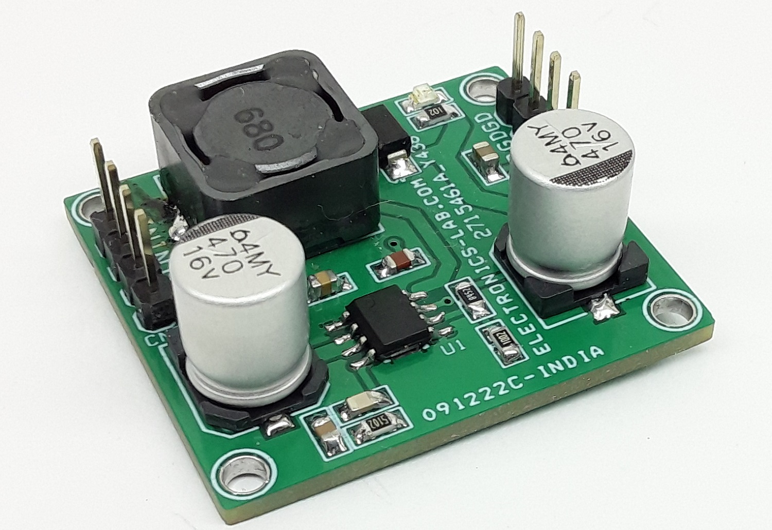
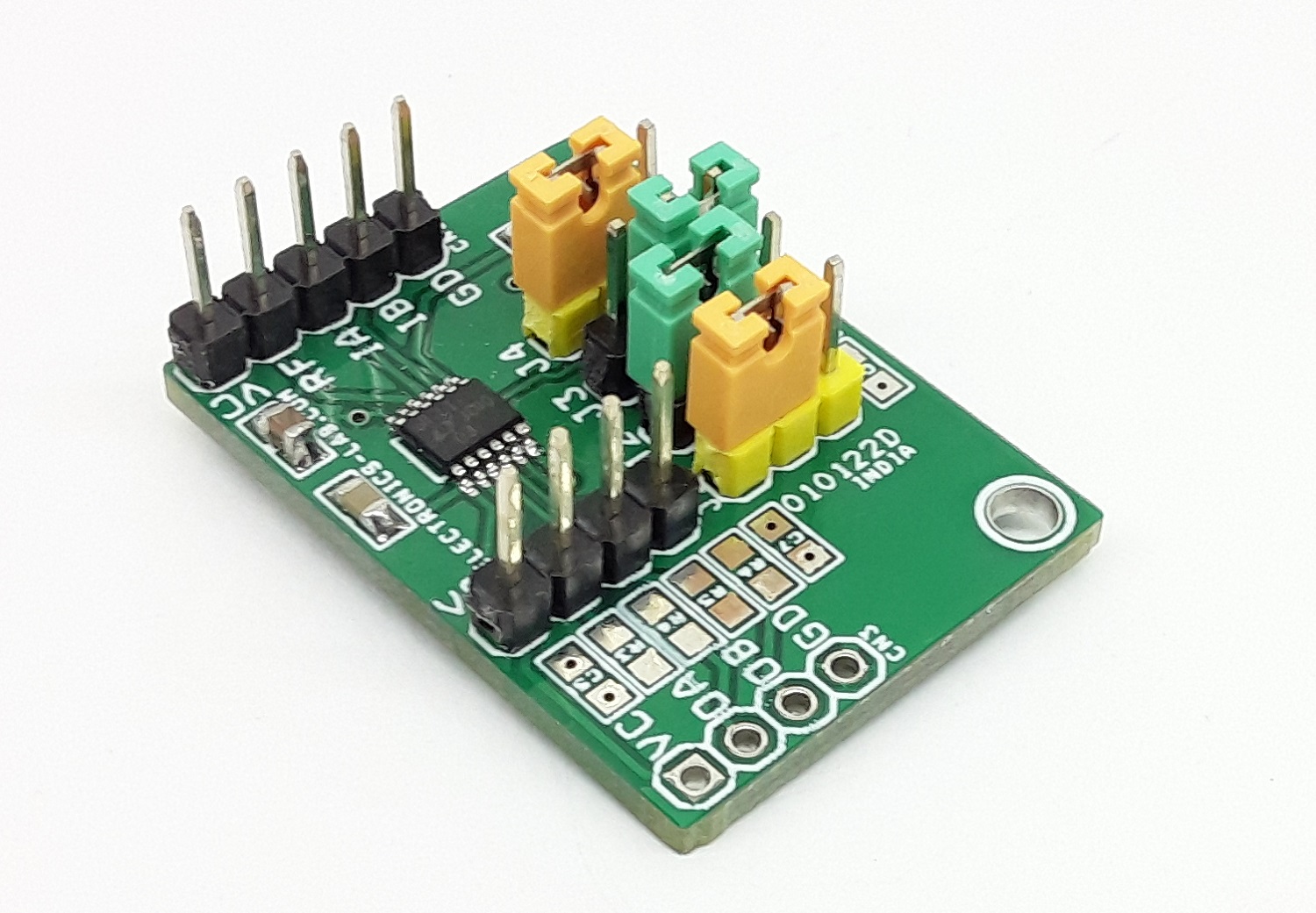
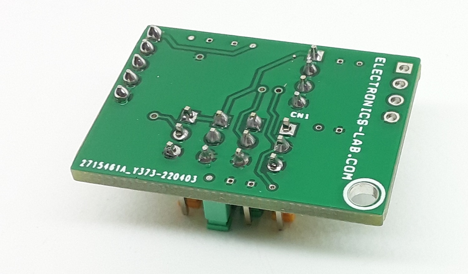
Photos