Analog Devices Inc. ADTF3175 1-MegaPixel Time-of-Flight Module

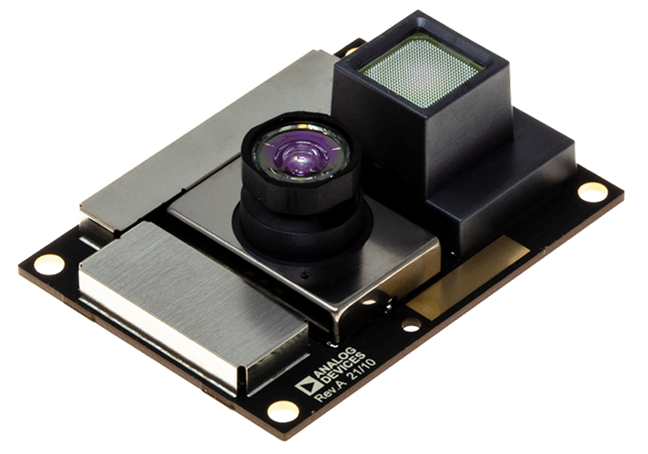
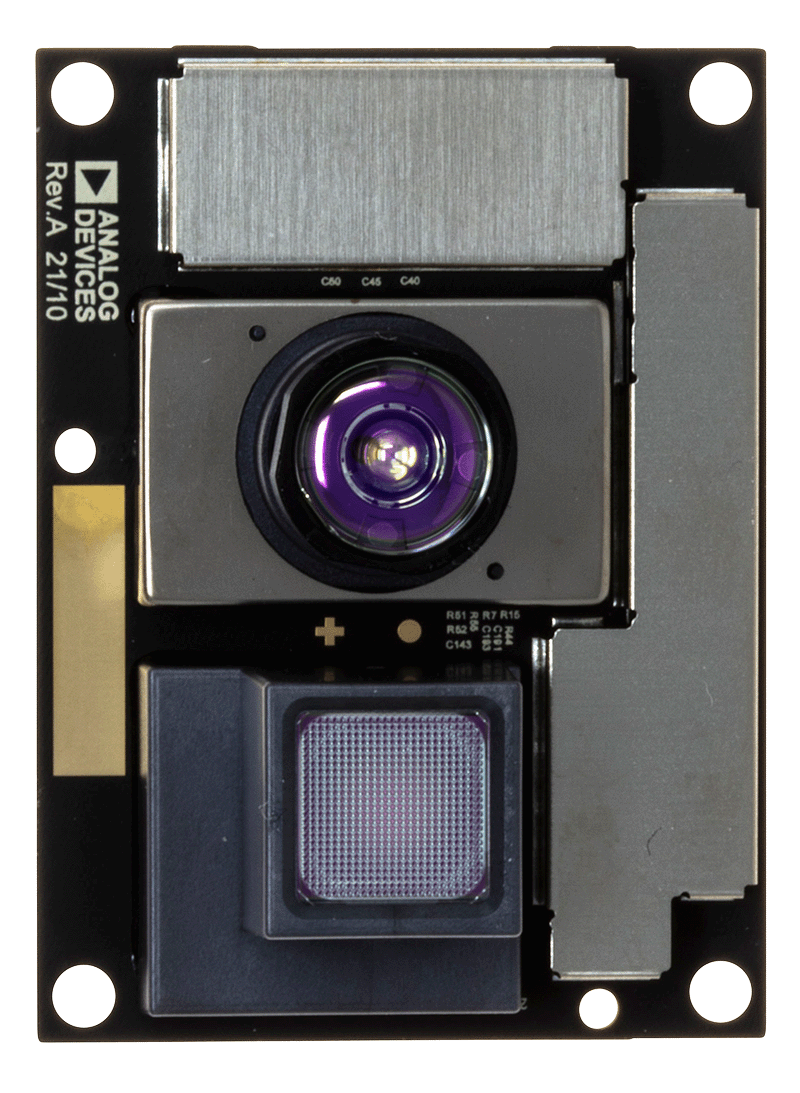
Analog Devices ADTF3175 1-MegaPixel Time-of-Flight Module is based on the ADSD3100, a 1-Megapixel CMOS indirect Time-of-Flight (iToF) imager and designed for high-resolution 3D depth sensing and vision systems. The ADTF3175 integrates a lens and optical bandpass filter for the imager, an infrared illumination source containing optics, a laser diode, a laser diode driver and photodetector, flash memory, and power regulators to generate local supply voltages. Fully calibrated at multiple range and resolution modes, the raw image data from the ADTF3175 is processed externally by the host system processor or depth ISP to complete the depth sensing system.

The ADTF3175 image data output interfaces electrically to the host system over a 4-lane mobile industry processor interface (MIPI), Camera Serial Interface 2 (CSI-2) Tx interface. The module programming and operation are controlled through 4-wire SPI and I2C serial interfaces. The Analog Devices ADTF3175 1-MegaPixel Time-of-Flight Module measures 42mm × 31mm × 15.1mm and operates over a -20°C to +65°C temperature range.

Features

  • 1024 × 1024 ToF imager with 3.5µm × 3.5µm pixels
  • 75° × 75° Field of view (FOV)
  • Imager lens subassembly with 940nm bandpass filter
  • Illumination subassembly with eye safety support
  • 4-lane MIPI CSI-2 Tx interface, 1.5Gbps per lane
  • 4-wire SPI and 2-wire I2C serial interfaces
  • NVM (Flash) for the module boot-up sequence
  • Power regulators for the local imager and illumination rails
  • Calibrated modes at 1024 × 1024 and 512 × 512 resolutions
  • 0.4m to 4m depth range (depth noise 15mm maximum, 15% minimum reflectivity, <5klux equivalent sunlight)
  • ±3mm depth accuracy (across full depth range)

more information: https://www.analog.com/en/products/adtf3175.html

Microchip’s MCP9700 and MCP9701 low-power linear active thermistor ICs provide a low-cost solution

Microchip’s low-power MCP9700, MCP9700A, MCP9700B, MCP9701, and MCP9701A analog temperature sensors with linear active thermistor integrated circuit (IC) convert temperature to analog voltage. These sensors have accuracy of ±1°C from +20°C to +70°C (MCP9700B), ±2°C from 0°C to +70°C (MCP9700A and MCP9701A), and ±4°C from 0°C to +70°C (MCP9700 and MCP9701) and consume 6 µA (typical) of operating current. These sensors provide a low-cost solution for applications requiring relative temperature change measurement.

Features

  • Available packages:
    • SC70-5, SOT-23-3, and TO-92-3 (not available with the MCP9700B)
  • Wide temperature measurement range:
    • -40°C to +125°C (extended temperature)
    • -40°C to +150°C (high temperature)
  • Accuracy:
    • ±1°C (max.), +20°C to +70°C (MCP9700B)
    • ±2°C (max.), 0°C to +70°C (MCP9700A and MCP9701A)
    • ±4°C (max.), 0°C to +70°C (MCP9700 and MCP9701)
  • Tiny analog temperature sensor
  • Optimized for analog-to-digital converters (ADCs):
    • 10 mV/°C (typical) (MCP9700, MCP9700A, and MCP9700B)
    • 19.5 mV/°C (typical) (MCP9701 and MCP9701A)
  • Wide operating voltage range:
    • VDD = 2.3 V to 5.5 V (MCP9700, MCP9700A, and MCP9700B)
    • VDD = 3.1 V to 5.5 V (MCP9701 and MCP9701A)
  • Low operating current of 6 µA (typical)
  • Optimized to drive large capacitive loads

more information: https://www.microchip.com/en-us/product/MCP9700A

IT8500G+ Series DC Electronic Load

ITECH’s IT8500G+ series programmable DC electronic load for ATE systems and component testing

ITECH’s IT8500G+ series, with a sampling bandwidth of up to 300 KHz, is a programmable DC electronic load specifically designed for high-precision ripple testing. With the built-in ripple test function, it is easy to measure voltage and current ripple of the DUT. IT8500G+ has as many as eight fast charging protocols built-in, meeting the test requirement of fast charging adapters, power banks, fast charging power banks, and other products. At the same time, it also has other functions like automatic testing, battery discharge testing, dynamic testing, and more, so it can complete most of the performance testing of switching power supplies, batteries, and other products during the development and production stages.

Features

  • Seven operating modes: CC/CV/CR/CW/CR+CC/CV+CC/CR-LED
  • Built-in voltage ripple and current ripple measurement function
  • Dynamic mode up to 20 kHz
  • Measurement resolution up to 0.1 mV/0.1 mA
  • Professional multi-channel mode, which can cascade up to 16 devices to reduce the cost of burn-in testing
  • Battery discharge mode, providing three cut-off conditions of time, voltage, and capacity
  • OPP/OCP test functions, suitable for power module protection function test
  • Automatic test function, widely used in adapter test
  • List function, which can simulate complex current carrier waveforms
  • Current monitoring function, without an expensive current probe, easy to realize current waveform monitoring (0 V to 10 V)
  • Short-circuit mode/measure function

more information: https://www.itechate.com/en/product/dc-electronic-load/IT8500Gplus.html

DRV8317 3-Phase PWM Motor Driver

Texas Instruments’ integrated MOSFET driver is suitable for driving 3-phase motors

Texas Instruments’ DRV8317 3-phase PWM motor driver provides three integrated MOSFET half-bridges for driving 3-phase brushless DC (BLDC) motors with 5 V, 9 V, 12 V, or 18 V DC rails or 2s to 4s batteries. The driver provides integrated 3-phase current sensing, eliminating the need for external sense resistors. The DRV8317 has an integrated LDO that provides a regulated 3.3 V rail that can deliver up to 80 mA for external loads such as microcontrollers (MCUs), logic circuits, hall sensors, and more. The configurable 6x or 3x PWM-control scheme can implement a sensored or sensorless field-oriented control (FOC), sinusoidal control, or trapezoidal control using an external MCU.

The DRV8317 can drive a PWM frequency of up to 200 kHz and is highly configurable through the SPI (DRV8317S) or pins (DRV8317H). The configurable features include PWM mode, slew rate, current-sense gain, and more. The integrated protection features include supply undervoltage lockout (UVLO), overvoltage protection (OVP), charge-pump undervoltage (CPUV), overcurrent protection (OCP), overtemperature warning (OTW), overtemperature shutdown (OTS), and protects the device, motor, and the system against fault events which are indicated by the nFAULT pin.

Features

  • 3-phase BLDC motor driver:
    • Configurable slew rate for EMI mitigation
    • Programmable gain current sensing
    • Supported PWM frequency: up to 200 kHz
    • Integrated shoot-through protection
  • Operating voltage range: 4.5 V to 20 V (24 V abs. max.)
  • High output current capability: 5 A peak-current drive
  • Low on-state resistance MOSFETs: RDS(ON) (HS + LS) at TA = +25°C : 130 mΩ (typ.)
  • Ultra-low Q-current sleep mode: 3 µA (max.) at VVM = 12 V, TA = +25°C
  • Built-in 3.3 V ±4.5%, 80 mA LDO regulator
  • Multiple control interface options: 6x PWM and 3x PWM
  • Integrated current sensing:
    • No external current-sense resistor is required
    • 3-phase current sense outputs
  • SPI and hardware device variants:
    • 10 MHz SPI interface variant for flexibility
    • Pin-configurable variant for simplicity
  • Supported logic inputs: 1.8 V, 3.3 V, and 5 V
  • Integrated protection features:
    • VM UVLO, VM OVP, CPUV, OCP, and OTW/OTS
    • Fault-condition indication pin (nFAULT)

more information: https://www.ti.com/product/DRV8317

BD14210G ±1% Accuracy Current Sense Amplifier

ROHM’s current sensing IC has a space-saving design that decreases the mounting area by 46%

ROHM’s BD14210G-LA current sense amplifier guarantees long time support in the industrial market. This device operates from a single 2.7 V to 5.5 V power supply. It has a wide common-mode voltage range of -0.2 V to +26 V, an output analog voltage, and a gain of 20 V/V. The matched gain resistor minimizes gain error and realizes low offset voltages. The input bias current is 1 µA (typ.) in typical conditions. There is no need to adjust the gain error.

The BD14210G-LA incorporates all required peripheral components. This simplifies current sensing by connecting a shunt resistor and a bypass capacitor. Furthermore, reducing the number of components from eleven to just three compared to conventional configurations (operational amplifier + discrete components). This amplifier decreases the mounting area by 46% (SSOP6 package).

This current sense amplifier features a highly accurate current detection of ±1% that can be achieved over the entire temperature range of -40°C to +125°C. The internal circuitry prevents current detection accuracy to decrease even when an external RC filter circuit for noise suppression is added. This minimizes the number of work-hours required for design. The wide input voltage range makes the BD14210G-LA ideal for current sensing applications operating from 12 V/24 V power supplies.

Features

  • Wide input voltage range: -0.2 V to +26 V
  • High accuracy current detection of ±1%
  • Low offset voltage: 1 µA (typ.)
  • Low input bias current
  • Space-saving design decreases the mounting area by 46% (SSOP6 package)

more information: https://www.rohm.com/products/sensors-mems/current-sensor-ics/current-sense-amplifier/bd14210g-la-product

Thermal Cutoff Overtemperature (TCO) Protection Devices – AD & SD Series

Bourns’ TCO mini-breaker devices are tested to AEC-Q200-listed stress tests

AD and SD series resettable miniature thermal cutoff (TCO) mini-breaker devices from Bourns, Inc. are the first TCO devices tested by Bourns to AEC-Q200-listed stress tests. The AD and SD series’ advanced overtemperature protection technologies make them ideal solutions for a broad variety of applications such as heaters, motors, cables, and printed circuit board components. They also offer excellent overtemperature protection for lithium-ion batteries in notebook PCs, tablets, smartphones, and power banks. The AD and SD feature high current and low resistance (less than 4 mΩ) in either a surface mount (SD) or axial-leaded/weldable (AD) package. Both series offer the option for the TCO device to be either non-automatically resettable (self-hold function) or automatically resettable (non-self-hold function).

Features

  • Miniature package size
  • Surface-mount package option
  • Superior overtemperature and overcurrent protection
  • Controls abnormal, excessive current virtually instantaneously, up to rated limits
  • Currently the industry’s widest range of trip temperatures, up to +150°C
  • High corrosion resistance
  • AEC-Q200 compliant

Applications

  • Heaters
  • Motors
  • Battery packs
  • Lithium-ion batteries in PCs, tablets, smartphones, and power banks

more information: https://www.bourns.com/docs/technical-documents/featured-product-bulletins/Bourns_KLM2209_SD_AD_NPR.pdf

ET980 COM Express Module with 12th Gen Intel Core Processors for Edge Computing

IBASE Technology Inc, a world leader in the manufacture of embedded boards and solutions, has added the ET980 series of COM Express modules to its portfolio. Supporting the U-series and P-series of 12th Gen Intel® Core™ processors from i3-1220PE to i7-1265UE (12M Cache, up to 4.70GHz), ET980 provides a platform with 10-12% boost in productivity performance compared with the previous generation. It is especially suited for applications demanding responsive technology to handle compute-intensive tasks simultaneously, such as medical instruments, industrial automation and control, robotics, and embedded gaming.

ET980 FEATURES:

  • Onboard 12th Gen Intel® Core™ i7/i5/i3 processors
  • 2x DDR4-3200 SO-DIMM sockets, Max. 64GB
  • Onboard 2.5 GbE
  • Supports 3x independent displays via HDMI / DP / VGA / LVDS or eDP
  • 4x USB 3.2, 8x USB 2.0, 2x SATA III, 2x COM
  • 1x PCI-E(x16), 1x PCI-E(x4), 4x PCI-E(x1) to carrier board
  • Digital I/O, TPM (2.0), Watchdog timer

The ET980 offers fast data transmission with an Intel® I226LM 2.5 GbE controller that is Time Sensitive Networking (TSN) capable. The integrated Intel® UHD Graphics drives independent display outputs (HDMI, DP, VGA, LVDS or eDP) to boost productivity levels. Two DDR4 SO-DIMM sockets are available with a capacity of 64GB to meet the needs of demanding real-time applications. The COM Express Type 6 module also supports 4x USB 3.2, 8x USB 2.0, 2x SATA III, 2x COM ports and 1x PCI-E(x16), 1x PCI-E(x4), 4x PCI-E(x1) expansion via the carrier board.

“The new ET980 COM Express module is ideally suitable for use in high-performance IoT edge computing and offers our customers the shortest time to market,” said Wilson Lin, Director of IBASE Product Planning Department. “Its upgradability and versatile design provide a competitive advantage, enabling lower cost of ownership through high configurability and optimum scalability.”

more information: www.ibase.com.tw

Discover LEMO’s new 12G-SDI 4K Ultra High Definition transmission push-pull connectors

LEMO is thrilled to announce the expansion of its field-proven S Series push-pull connectors with the new 1S.275 Series for 12G-SDI (Serial Digital Interface) 4K Ultra High Definition transmission. The new robust push-pull connectors are compliant with the SMPTE ST 2082-1 standard for signal/data transmission and enable a transmission rate of 12 Gbit/s meeting the 12G-SDI transmission standard and providing eight times the bandwidth of a standard HD-SDI in a single link. The chocolate bar shape makes it easier to grip and handle with ease.

LEMO has developed these connectors in response to the rapidly advancing technology landscape and market demands for high transmission rates, lighter structure, low-latency in live events for the Audio Video Broadcasting (AVB) market segments and other market segments like medical imaging platforms such as endoscopy and laparoscopy, among others.

The optimum design of these connectors ensures seamless transmission with high precision, reliability, low return loss, making it a viable alternative to using dual 6G or Quad 3G links. Currently, many 4K professional cameras use Quad link BNC connectors to transmit 12G signals for UHD displays. The newly introduced LEMO product will facilitate the transmission of 12G-SDI using a compact single link connection for UHD displays, enabling higher panel density thus reducing the number of cables/ connectors.

Thanks to its expertise and cable assembly capabilities, LEMO is at your disposal to assist you in providing complete interconnect solutions.

Find out more on: www.lemo.com

Texas Instruments bq25628/bq25629 Battery Charger ICs

Texas Instruments bq25628/bq25629 Battery Charger ICs are highly-integrated 2A switch-mode battery charge management and system power path management devices for single-cell Li-ion and Li-polymer batteries. The solution is highly integrated with built-in current sensing, loop compensation, input reverse-blocking FET (RBFET, Q1), high-side switching FET (HSFET, Q2), low-side switching FET (LSFET, Q3), and battery FET (BATFET, Q4) between system and battery. The device uses narrow VDC power path management, regulating the system slightly above the battery voltage without dropping below a configurable minimum system voltage. The low impedance power path optimizes switch-mode operation efficiency, reduces battery charging time, extends battery life during discharging phase, and the ultra-low 0.15µA ship mode current extends battery shelf life. The I2C serial interface with charging and system settings makes bq25628 and bq25629 truly flexible solutions.

The bq25628 supports a wide range of input sources, including a standard USB host port, USB charging port, and USB-compliant high-voltage adapter. The bq25629 has the ILIM pin to set the default input current limit and TS_BIAS pin for controlled thermistor bias. The device complies with USB 2.0 and USB 3.0 power specifications for input current and voltage regulation and meets the USB On-the-Go (OTG) operation power rating specification up to 2.0A

Features

  • High-efficiency, 1.5MHz, synchronous switching mode buck charger for single-cell battery
    • >90% efficiency down to 25mA output current from 5V input
    • Charge termination from
    • Flexible JEITA profile for safe charging over temperature
  • BATFET control to support a shutdown, ship mode, and full system reset
    • 1.5µA quiescent current in battery-only mode
    • 0.15µA battery leakage current in ship mode
    • 0.1µA battery leakage current in shutdown
  • Supports Boost Mode operation to power accessory
    • Boost Mode operation supporting 3.84V to 5.2V output
    • >90% boost efficiency down to 100mA boost current for 5V PMID
  • Supports a wide range of input sources
    • 3.9V to 18V wide input operating voltage range with 26V absolute maximum input voltage
    • Maximizes source power with input voltage regulation (VINDPM) and input current regulation (IINDPM)
    • VINDPM threshold automatically tracks battery voltage
  • Efficient battery operation with 15mΩ BATFET
  • Narrow VDC (NVDC) power path management
    • System instant-on with depleted or no battery
    • Battery supplement when the adapter is fully loaded
  • Flexible autonomous or I2C-controlled modes
  • Integrated 12-bit ADC for voltage, current, and temperature monitoring
  • High Accuracy
    • ±0.4% charge voltage regulation
    • ±5% charge current regulation
    • ±5% input current regulation
  • Safety
    • Thermal regulation and thermal shutdown
    • Input, system, and battery overvoltage protection
    • Battery, and converter overcurrent protection
    • Charging safety timer

Application Circuit

Texas Instruments bq25628/bq25629 provides various safety features for battery charging and system operations, including battery negative temperature coefficient thermistor monitoring, charging safety timer, and overvoltage and overcurrent protections. The thermal regulation reduces the charge current when the junction temperature exceeds the programmable threshold. The STAT output reports the charging status and any fault conditions. Other safety features include battery temperature sensing for charge mode and OTG boost mode, thermal shutdown and input UVLO, and overvoltage protection. The INT output notifies the host when a fault occurs or status changes. The bq25628 and bq25629 are available in an 18-pin, 2.5mm × 3.0mm WQFN package.

more information: https://www.ti.com/product/BQ25628

Energy harvesting PMIC from Nexperia includes MPPT tracking

Nexperia, the expert in essential semiconductors, today announced an expansion to its range of Power ICs with Energy Harvesting solutions to simplify and enhance the performance of low-power internet of things (IoT) and other embedded applications. The NEH2000BY is a high-performance power management integrated circuit (PMIC) which recharges a battery or storage capacitor using energy harvested from ambient sources, such as light (which can be harvested using a photovoltaic cell). As a result, Nexperia’s NEH2000BY will enable the development of electronic devices that are self-powered, smaller, and environmentally friendly. Furthermore, this energy harvesting solution can help mitigate the environmental impact of the billions of batteries produced and discarded each year.

Nexperia’s NEH2000BY PMIC makes it much easier to design energy harvesting solutions which can be up to 20x smaller than other competing offerings and do not require manual optimization for individual applications. In addition, the PMIC was designed without inductors, simplifying PCB design, and significantly reducing overall BOM and board size, with a 12 mm² assembly area.

To achieve the highest conversion efficiency, energy harvesting solutions must be able to adapt as the ambient energy source fluctuates. The NEH2000BY performs Maximum Power Point Tracking (MPPT), an adaptive algorithm to optimize how it transfers harvested energy and to achieve optimum average conversion efficiency by up to 80%. This unique MPPT algorithm combines speed with accuracy, allowing the PMIC to adapt to environmental changes in less than a second. This is significantly faster than any other currently available solution and maximizes the amount of energy harvested over the course of a day, vastly expanding the number of application areas. Furthermore, due to its self-optimization functionality and ability to operate autonomously without the requirement for pre-programming, the NEH2000BY makes it easier for designers to power devices with ambient energy.

Nexperia’s energy harvesting solutions enable economical energy harvesting from various ambient sources in applications consuming up to several milliwatts of power, including wireless IoT nodes, wearable smart tags, and electronic shelf labels.

Dan Jensen, General Manager Business Group Analog & Logic IC’s at Nexperia adds,

“The NEH2000BY’s cost-efficient, user-friendly, and compact nature will allow the adoption of energy harvesting in a larger range of use cases. By eliminating the requirement to change batteries in these applications, NEH2000BY will significantly reduce the amount of hazardous waste produced, with enormous environmental benefits.”

The NEH2000BY is available in a 16-lead, 3 mm × 3 mm QFN package and operates between -40°C and +85°C.

To learn more about our new product, please visit our website at www.nexperia.com/product/NEH2000BY or read the blog post for more in-depth information: https://efficiencywins.nexperia.com/efficient-products/adaptive-energy-harvesting-pmic.

TOP PCB Companies