Sequans Monarch Go Certified LTE IoT Category M1 Modems, connected by Verizon, are comprehensive modem components offering a short route to market and a low Total Cost of Ownership (TCO) to develop cellular-IoT connected devices. The Monarch Go Modems avoid costly lab testing while improving time-to-market thanks to a reduced effort for board design. These modems remove the need to design and tune a cellular antenna as it embeds an optimized LTE antenna, saving months of design effort and lab testing. The plug-and-go Monarch Go Modems feature a pre-installed ThingSpace IoT SIM and a default data plan.
The mechanical integration of the Monarch Go LTE-M modem component into IoT devices is extremely simple, requiring only two screws, a single low-profile board-to-board connector, and no soldering. Monarch Go includes an industry-standard UART interface, a set of AT commands, and examples for connecting your device application MCU controller.
Features
LTE-M modem component with embedded antenna certified for use on the Verizon network
Optional embedded GPS
ThingSpace IoT SIM pre-installed
ThingSpace online management
Easy connection to cloud services from a third party and geolocation
Industry-leading network coverage in the USA
RoHS compliant
Specifications
Modem
Sequans Monarch™ LTE-M chip
Pre-installed ThingSpace IoT SIM
Certified for use on the Verizon network (LTE band 13) with a roadmap for global band support
Compatible with Linux, Windows, and a wide range of embedded and real-time operating systems
High-speed UART as data and AT command interface
Embedded IP stack with support for UDP, TCP, TFTP, FTP, HTTP, HTTPS, MQTT, or MQTTS
Location based services
SMS send and receive
Low power modes PSM, eDRX, and RRC IDLE
Support for Verizon FOTA services from the ThingSpace online management platform
LTE Cat M1: 375kbps uplink and 300kbps downlink (peak)
LTE-M data plan
Verizon LTE-M data plans available from the ThingSpace online management platform
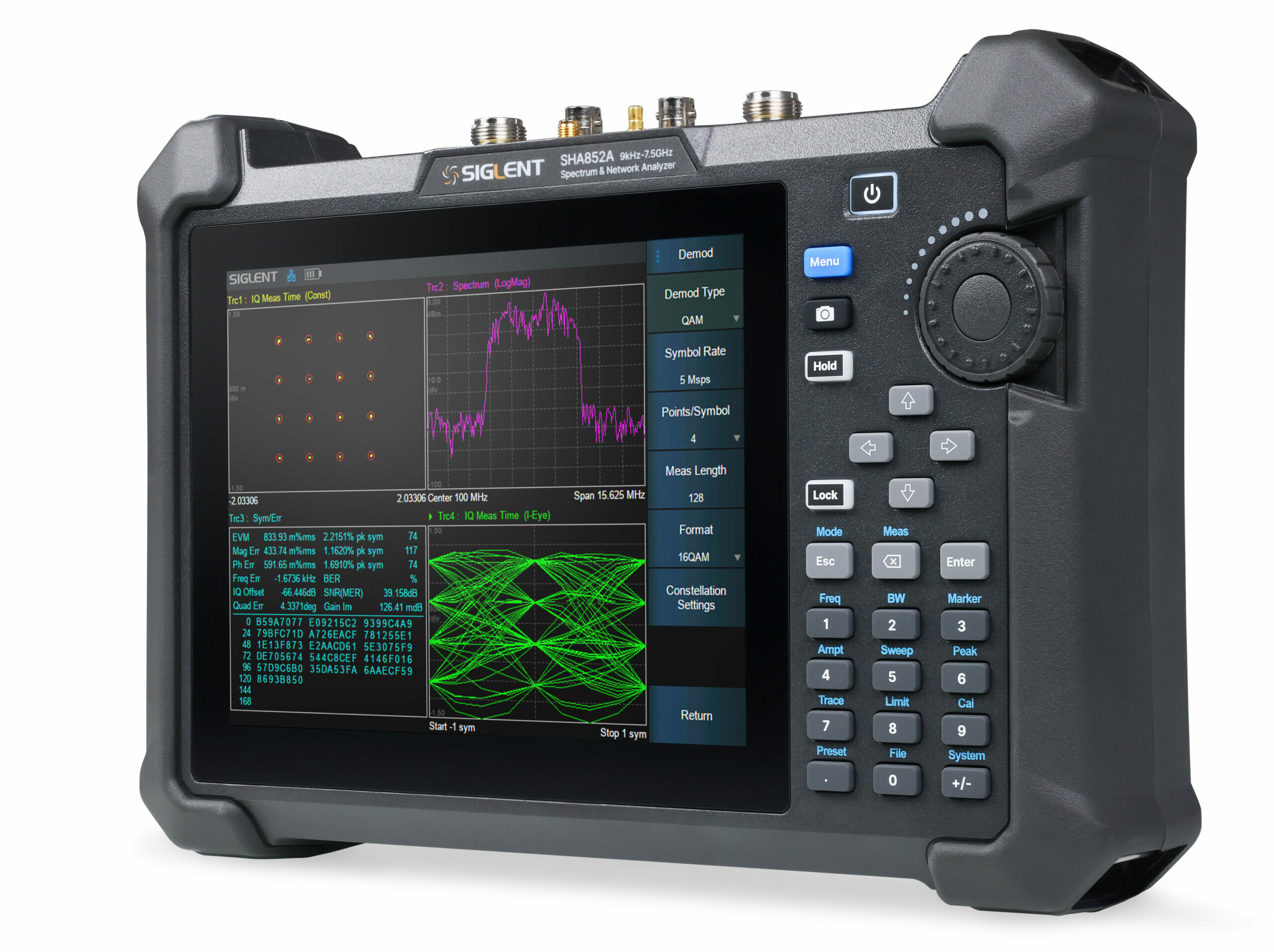
Siglent SHA800A analyzers combine the capabilities of a Spectrum Analyzer, a Vector Network Analyzer, and a Cable/Antenna Tester all in one intuitive handheld package. With a frequency range up to 7.5 GHz, these analyzers deliver reliable automatic measurements and multiple modes of operation.
Saelig Company, Inc. has introduced the SIGLENT SHA800A series, handheld portable spectrum analyzers which form a powerful, versatile choice for benchtop and field RF measurement applications. SHA800A analyzers combine the capabilities of a Spectrum Analyzer, a Vector Network Analyzer, and a Cable/Antenna Tester all in one intuitive handheld package. With a frequency range up to 7.5 GHz, these analyzers deliver reliable automatic measurements and multiple modes of operation. The spectrum analyzer includes a built-in amplifier and independent signal source, fast scanning speed, high sensitivity. It can monitor RF broadcasts, perform channel power scanning, power monitoring, wireless interference location, electromagnetic compatibility measurements, and other functions. The cable and antenna testing function includes built-in DC voltage bias, with a 1-path-2-port vector network analysis function. It can measure TDR, VSWR, debug port matching issues, perform insertion loss measurements, tower amplifier debugging, cable fault location, Smith charts, etc.
With two models (SHA851A/SHA852A) the specifications include:
Minimum Resolution Bandwidth (RBW) 1 Hz up to 10 MHz
Preamplifier and independent signal source up to 7.5 GHz,
GPS positioning and logging
Cable and Antenna Test
Frequency Range from 100 kHz up to 3.6/7.5 GHz,
Distance To Fault and Time Domain Analysis
Vector Network Analyzer
Bias out up to 32VDC
Typical working time 4 hours,
Weight 7lb
8.4” Multi-Touch Screen, Mouse and Keyboard supported
The explosion of RF Technologies such as 5G and IoT has created a highly complex electronic measurement environment. Monitoring and debugging these applications are increasingly shifting from laboratories and workstations to on-site and outdoor applications, requiring reliable handheld measurement instruments. Applications for the SHA800A analyzers include communication engineering, telecom operation and maintenance, radio management, factory production, education and teaching, and many others. They provide a capable and more economical alternative to other handheld analyzers. Siglent SHA800A Analyzers are available now from Saelig Company, Inc.
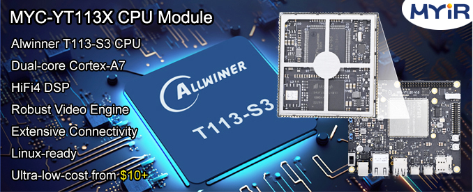
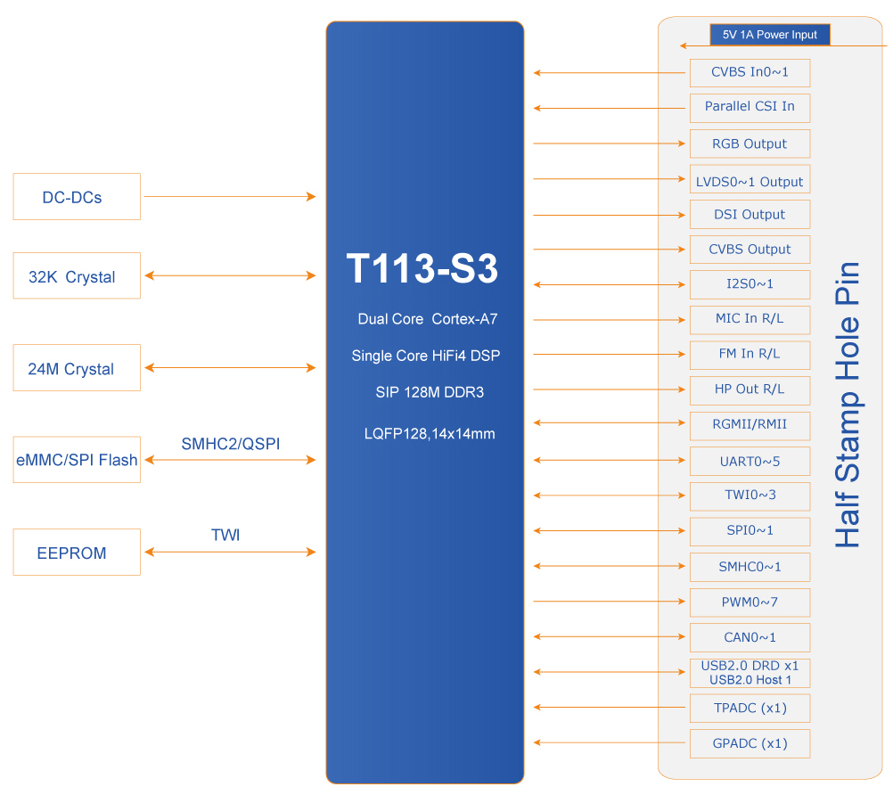
MYIR has launched a new SoM MYC-YT113X based on Allwinner SoC after introduced the MYC-YT507H for T507-H last year. The MYC-YT113X CPU Module is powered by Allwinner T113-S3 processor which features up to 1.2 GHz Dual-core ARM Cortex-A7 processor with 128MB DDR3 on-chip memory. Additionally, the MYC-YT113X takes more other advantages of the T113-S3 MPU such as the single-core HiFi4 DSP, Robust Video Engine and extensive connectivity to provide an ideal solution for smart control and HMI applications in the automotive and industrial sectors. MYIR offers two standard configurations for 256MB Nand Flash or 4GB eMMC external memory options. A number of peripheral and IO signals are access through 1.0mm pitch 140-pin stamp-hole (Castellated-Hole) expansion interface.
The MYC-YT113X CPU Module is a highly integrated SoM, measuring only 39mm by 37mm. It is capable of running Linux and provided with software resources including kernel and driver source code, together with detailed user manual and documentations to help customer start their development rapidly.
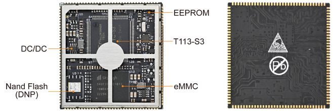
MYC-YT113X CPU Module Top-view and Bottom-view (delivered with shielding cover by default)
Features Of MYC-YT113X CPU Module
Dimensions: 39mm x 37mm
PCB Layers: 6-layer design
Power supply: 5V/1A
Working temperature: -40~85 Celsius (industrial grade)
Allwinner T113-S3 processor
– Up to 1.2GHz Dual-core Arm Cortex-A7 with built-in 128MB DDR3
– Single-core HiFi4 DSP
– Supports H.265/H.264 video decoding up to 1080p@60fps and JPEG/MJPEG video encoding up to 1080p@60fps
4GB eMMC or 256MB Nand FLASH
32KB EEPROM
0mm pitch 140-pin stamp hole expansion interface
– 1 x RGMII/RMII
– 2 x USB2.0
– 6 x UART
– 2 x CAN
– 4 x TWI
– 2 x SPI
– 1 x GPADC and 4 x TRADC
– 1 x MIPI DSI
– 1 x Single-channel LVDS and 1 x Dual-channel LVDS or 24-bit RGB (supports up to 1080p@60fps)
– 1 x RGB
– 1 x Parallel CSI
– 2 x I2S
– Up to 59 GPIOs (Note: the peripheral signals brought out to the expansion interface are listed in maximum number. Some signals are reused. Please refer to the processor datasheet and CPU Module pin-out description file)
Linux OS
MYC-YT113X CPU Module Function Block Diagram
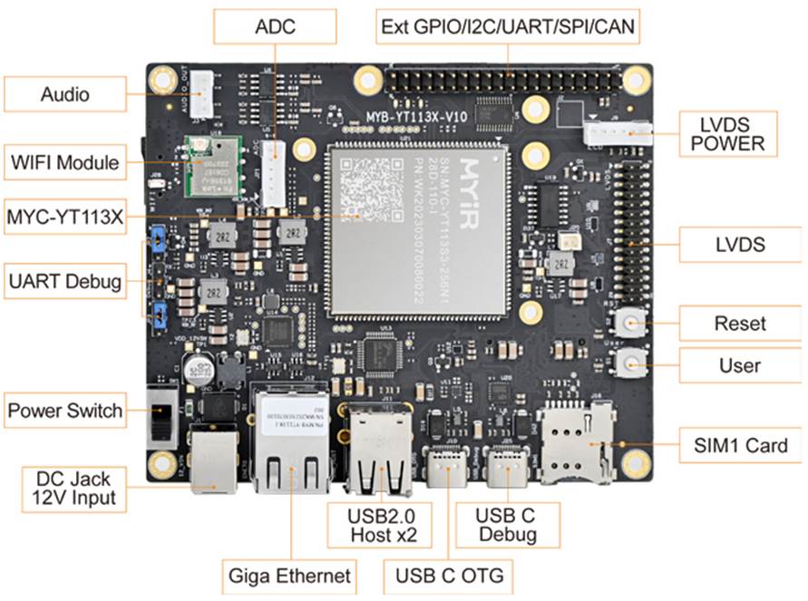
MYIR provides MYD-YT113X Development Board for evaluating the MYC-YT113X CPU Module. It has a versatile base board to facilitate the expansion from the MYC-YT113X through the 140-pin interface, such as serial ports, USB, Ethernet, CAN, WiFi, LVDS, Audio and so on. It is an excellent evaluation platform as well as a solid reference design for customers using the MYC-YT113X CPU Module or solutions based on T113-S3 processors.
MYD-YT113X Development Board Top-view
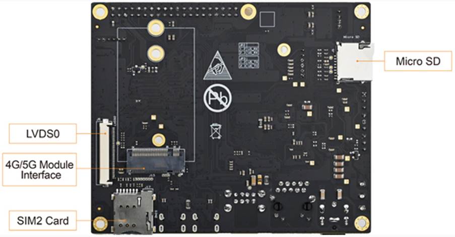
MYD-YT113X Development Board Bottom-view
The MYC-YT113X CPU Module is a high-performance and ultra-low-cost SoM, pricing at only $14/pc for the 256MB Nand Flash version (MYC-YT113S3-256N128D-110-I). Discount is to be offered for volume quantities. MYIR also provides OEM/ODM services to help customers accelerate their time to market and save cost.
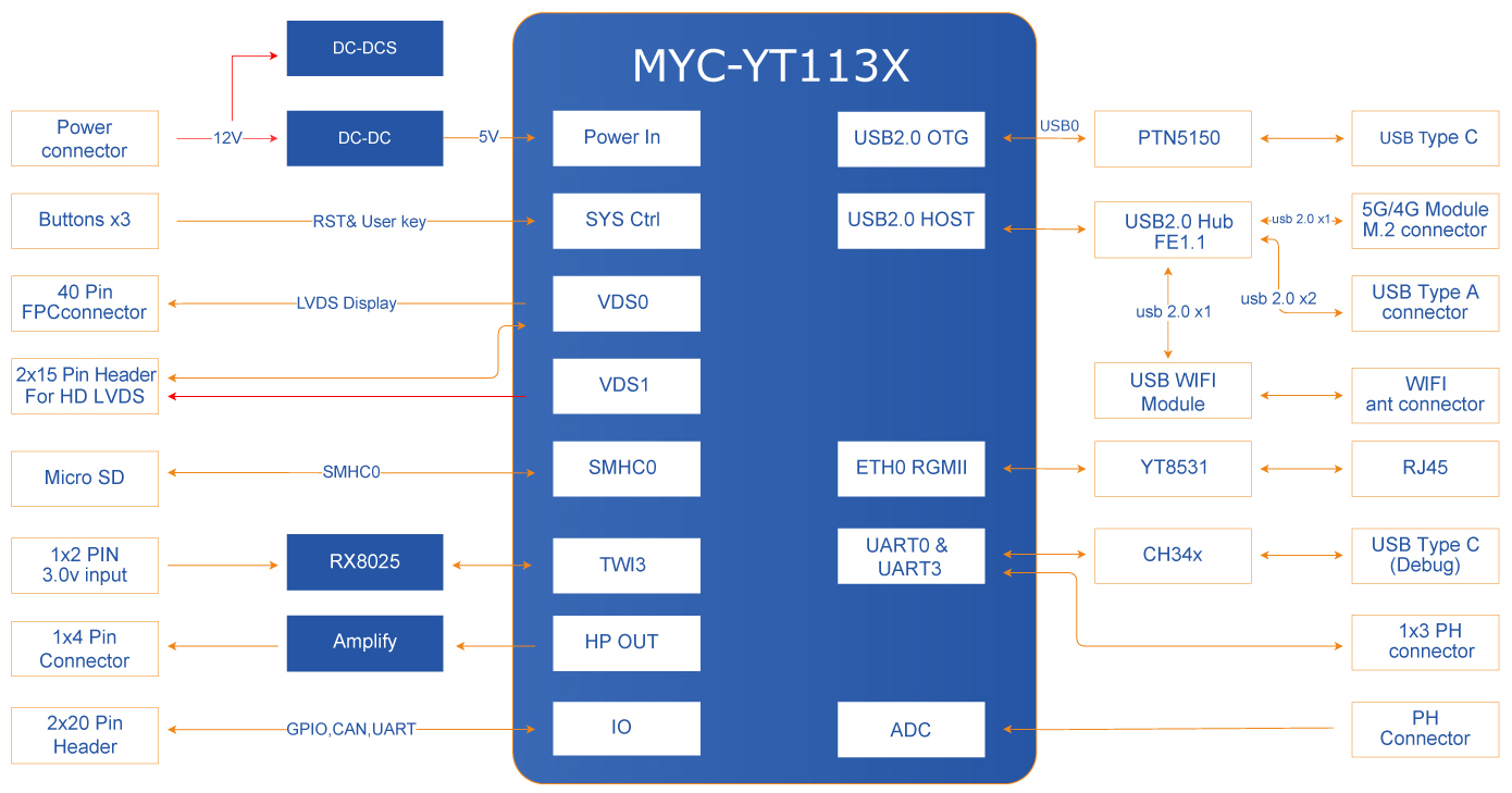
MYD-YT113X Development Board Function Block Diagram
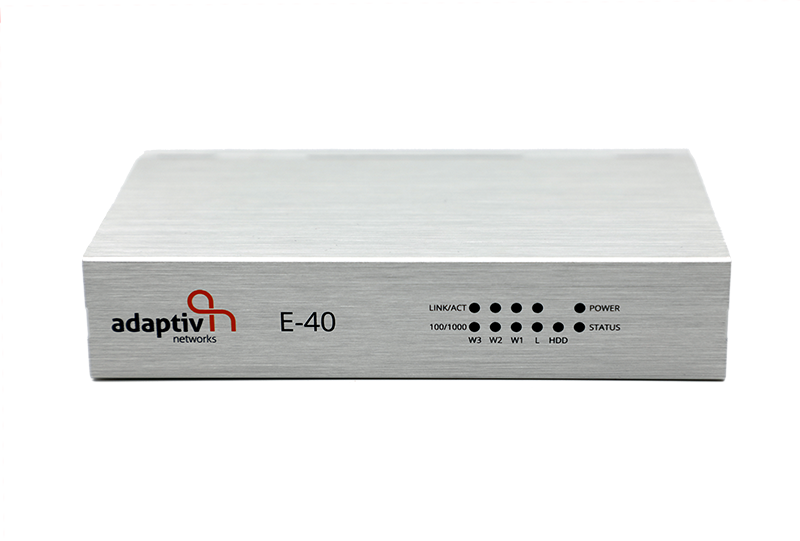
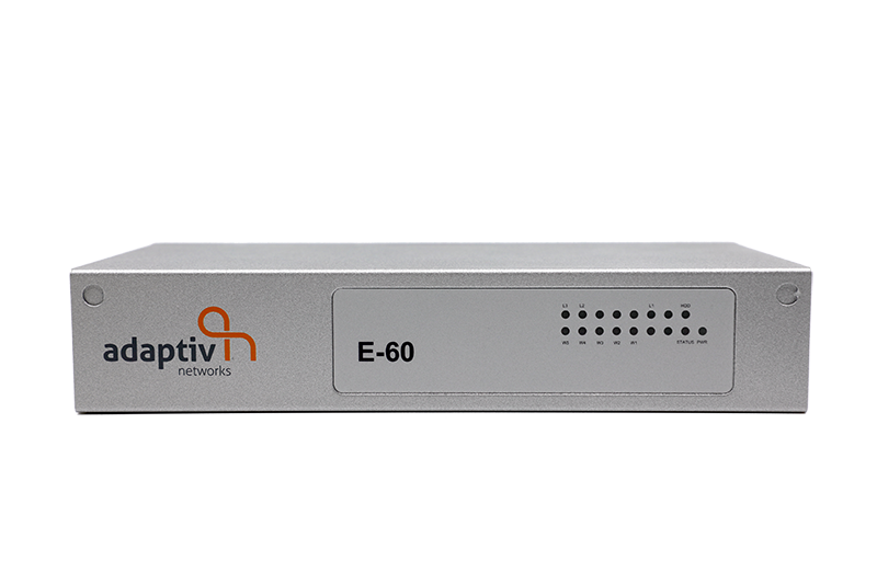
With network security a priority in the hybrid working world, AAEON and Adaptiv lead the way.
The value of the SD-WAN solutions market is projected to hit $13.7 billion worldwide by 2026, with more and more organizations making data security a priority. As one of the leading manufacturers of advanced network computing and security hardware platforms, AAEON seeks to make a big contribution in the attempt to achieve this market growth, with a greater focus on providing versatile and cost-effective networking solutions to the US market.
To do this, AAEON has strengthened ties with Adaptiv Networks, a leading cloud-native SD-WAN-as-a-Service vendor with whom AAEON has had a strong partnership for a number of years. In collaboration with Adaptiv, AAEON will help enterprises to simplify their network infrastructure, increase network performance, and improve security.
With its continuously expanding desktop and rackmount network appliance ranges, AAEON has demonstrated a commitment to innovation by incorporating the newest and most sophisticated Intel® platforms to give network security providers the most effective and market-ready white box solutions. This commitment has paid off in the past, with AAEON being awarded Gold Partner status in 2022’s Intel Network Builders Winners’ Circle Program, in recognition of its successful adoption and commercialization of Intel® architecture in its network platform solutions hardware.
Adaptiv’s SD-WAN solutions are designed to address the growing need for enterprises to securely connect to cloud applications and services. In addition to this, there is a growing emphasis on supporting remote and hybrid working environments, for which organizations must balance network functionality with data security. For industries with heightened privacy concerns, such as online platforms like kasyno wypłata bez weryfikacji, ensuring seamless and secure connectivity is crucial, as they must offer users not only convenience but also robust protection against potential data breaches.
The increased prevalence of SD-WAN and SaaS solutions illustrates a positive and necessary shift towards institutions prioritizing network security and reliability as hybrid working environments become the new norm. This is why AAEON chooses to work with elite providers like Adaptiv to ensure organizations receive the benefits that its white box solutions offer.
For more information about AAEON’s network appliance range, please visit our website or contact an AAEON representative directly.
For more information about Adaptiv’s award-winning cloud-managed network connectivity solutions, please visit their website.
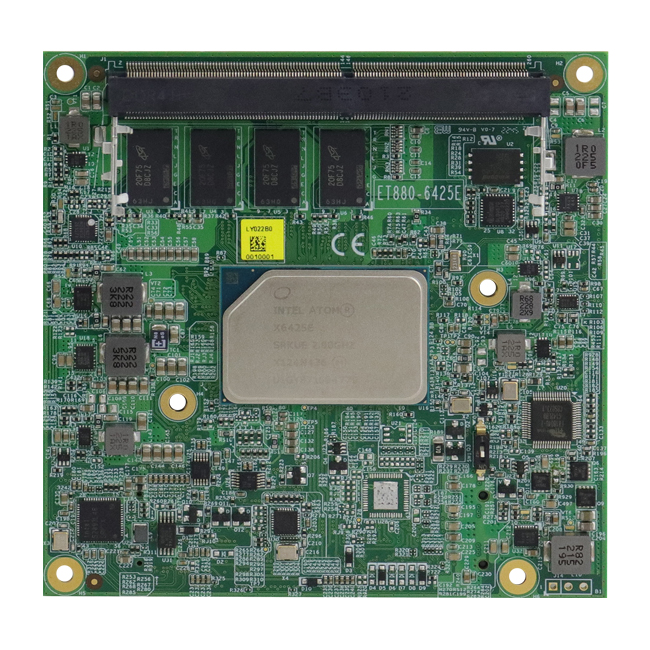
IBASE Technology Inc., a leading provider of industrial motherboards and embedded computing solutions, has announced the release of its latest ET880 COM Express CPU module designed to meet the demands of embedded applications that require low power consumption and fanless operation. The module integrated Intel Atom x6000 series processors that are built on 10nm technology support clock speeds of up to 3.2 GHz and Intel’s Time Coordinated Computing (TCC) technology, which enables precise clock synchronization across multiple devices.
The ET880 delivers robust performance and reliability, with features that make it an ideal choice for a variety of industrial and IoT applications. The module boasts onboard 8GB DDR4 memory and a DDR4 SO-DIMM slot for a total RAM capacity of 24GB to ensure efficient system operation. It is equipped with a range of connectivity options, such as a I226IT PCI-E 2.5G LAN controller, two USB 3.1, four USB 2.0, two SATA III, two UART (Tx/Rx only), and three independent displays via the DisplayPort / DVI-D / LVDS or eDP interfaces on the IBASE IP419 carrier board.
The ET880 is compatible with Windows 10 and Linux operating systems, and manufactured to meet the stringent requirements of industrial applications, with an extended temperature range of -40°C ~ +85°C, and long-term availability.
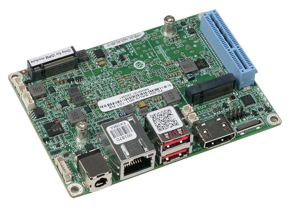
The high-performance Hyper-EHL board from ICP Germany is a cost-effective solution for applications requiring high reliability, such as industrial automation, machine control, traffic engineering and display systems.
The Hyper-EHL board can be purchased with two different Elkhard Lake CPUs: Variant one with Intel® Celeron J6412 offers four processor cores, a base clock frequency of 2.00 GHz, 1.5 MB cache and an Intel® processor graphics unit with 400 MHz, while variant two with Intel® Celeron N6210 brings two processor cores, 1.20 GHz base clock frequency, 1.50 MB cache an Intel® processor graphics unit with 250 MHz. An LPDDR4 working memory with 4GB is soldered onto the board. Optionally 8GB are possible from 100 pieces. An iSATA slot and an M.2 slot with M Key are available for mass storage.
Specifications
Pico-ITX board with Intel® Celeron J6412 or N6210 CPU
LPDDR4 4GB memory (optional 8GB)
Three independent displays: HDMI, Display Port and optional IDPM
2.5 GbE Intel® I225V
Two USB 3.2, two USB 2.0, one iSATA, one COM interface
Extensions: one M.2 M slot, one PCIe x4 slot
The Hyper-EHL has numerous connectors, including HDMI, Display Port, optional iDPM, a 2.5 GbE Intel® I225V LAN interface, two USB 3.0, two internal USB 2.0 and an internal RS232/422/485 interface. With a voltage input of 12V DC, the wafer EHL can be used in environments from 0°C to 60°C.
ICP Germany supplies the Hyper-EHL with appropriate memory and CPU on request.
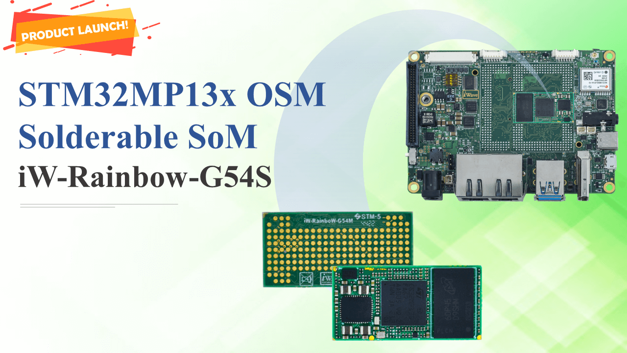
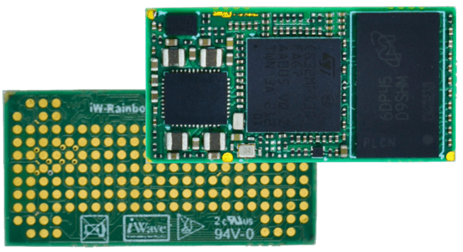
In line with the new industry standard, Open Standard Module or OSM, defined by SGET, iWave announces the release of the iW-RainboW-G54S: STM32MP13x LGA System on Module (SoM). The SoM incorporates STM32MP13x MPU from STMicroelectronics and is built on OSM Size-0 standard, providing high performance, power efficiency, and a rich set of interfaces to meet versatile market needs.
High-end wearables and other low-powered embedded & consumer applications benefit from the new STM32MP13x MPUs featuring the ARM Cortex-A7 application processors running at 1GHz. Cortex-A7 has all the features of the high-performance Cortex-A15 and Cortex-A17 processors, including physical virtualization, NEON, and 128-bit AMBA 4 AXI bus interfaces.
Key features of STM32MP13x OSM System on Module
STM32MP13x MPU with Arm Cortex-A7
Up to 1GB DDR3L, 16Mb QSPI NOR Flash
1 x RGMII, 1 x USB 2.0 OTG, 1 x USB 2.0 Host
2 x SDMMC, 2 x ADC
4 x UART, 1 x Console UART, 2 x SPI, 2 x I2S, 2 x I2C
16 x OSM GPIOs
Size-0 Form Factor: 30 mm x 15 mm
Solderable LGA Package in OSM v1.1 Standard
188 Contacts
The STM32MP13x System on Module is built on a 30 mm x 15 mm OSM Size-0 standard, the smallest size in the OSM variants making it an ideal choice for building portable consumer products. The 188 LGA contacts available on its back for mating with the carrier board make the platform resistant to shock and vibrations, ensuring high levels of robustness.
iWave brings design compactness while enabling modularity and scalability to ST customers. To fulfill the ever-increasing need for rapid data transfer, the SoM supports dual USB 2.0 interfaces and Gigabit Ethernet delivering a robust, high-performance, consistent, high-quality user experience.
Key features of STM32MP13x Single Board Computer
STM32MP13x MPU with Arm Cortex-A7
Up to 1GB DDR3L, 16Mb QSPI NOR Flash, 16Mb SPI NOR Flash
Micro SD, M.2 connector Key B (USB, Nano SIM connector)
Gigabit Ethernet (RGMII), USB 2.0 OTG, USB 2.0 Host
The System on Module forms the building block for products and solutions that require a rich set of interfaces with high performance and efficiency. The SoM enables customers to shorten their time to market with reduced risk and complexity.
“STM32MP13x MPU incorporating Cortex-A7 offers power and performance balance for a variety of devices with varying requirements,” said Ahmed Shameem, Hardware Project Manager at iWave Systems. “The STM32MP13x Solderable System on Module leverages the processor features to provide rich performance for diverse low-power embedded applications that ST customers require.”
STM32MP13x OSM SoM is mounted on a carrier board as a Single Board Computer (SBC), which can also be used as an evaluation kit. This feature-rich multimedia insert-ready SBC is available in Pico-ITX form factor, ready to be integrated across diverse machine learning applications.
The System on Module and Single Board Computer are go-to-market and production ready complete with documentation, software drivers, and a board support package. iWave maintains a product longevity program that ensures that modules availability for long periods of time (10+ years).
More information on STM32MP13x OSM System on Module can be found here.
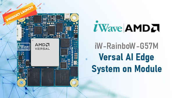
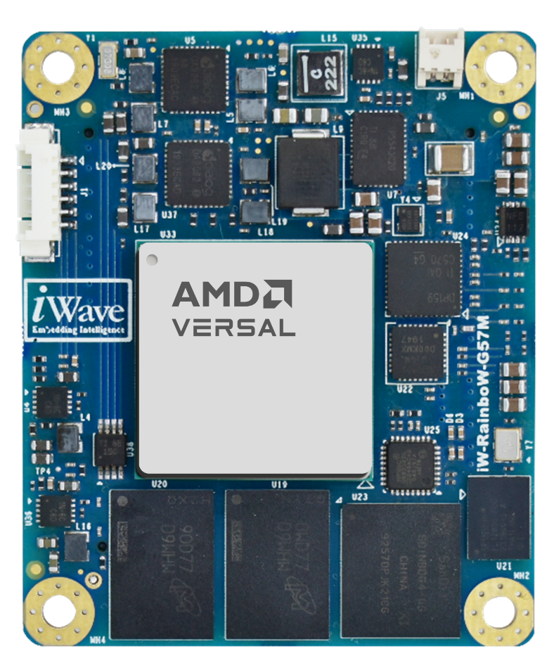
iWave introduces iW-Rainbow-G57M: a new System on Module (SOM) based on the AMD series, designed to power AI applications from the edge to the endpoint. The new SOM features the Versal AI Edge series to deliver leading AI performance/watt in the industry and provide the AI acceleration required for many applications ranging from ADAS and robotics to medical imaging.
iW-Rainbow-G57M: The Versal AI Edge-based System on Module is compatible with an extensive series of chips: VE2302/VE2202/VE2102/VE2002. The System on the Module is integrated with 8GB LPDDR4 RAM and 128 GB EMMC and 256MB QSPI Flash. Two high-speed expansion connectors and 122 User Configurable IOs provided on the System on Module enable a multitude of interfaces available for the user.
The Versal SOM supports a breadth of connectivity options, such as 28.21Gbps high-speed transceiver blocks to support all necessary protocols in edge applications, 40G multi-rate Ethernet, PCIe, and native MIPI support for vision sensors which are a must for advanced AI applications.
The Versal AI Edge provides the capability to run larger models and faster inference engines on the Edge. The Versal AI Edge combines scalar engines (Arm Cortex A72 Cores applications processor and Arm Cortex R5 core for real-time processing and control) enabling computing for complex algorithms while enabling high levels of safety and security. With the System on Module, customers can build their Edge AI Solution with reduced development cost, risk, and time. The System on Module also provides customers with the flexibility and scalability features of the Versal Edge AI series.
Dual-core Cortex-A72 Core and Dual-core Cortex-R5F Core
Up to 328K Logic cells & 150K LUTs
Up to 45 TOPA(INT4) AI compute
Programmable Network on Chip (NoC)
Up to 8GB LPDDR4, up to 128GB eMMC, 256MB QSPI
8 GTYP Transceiver support (VE2302 & VE2202).
GTYP support: PCIe Gen4 or 40G Multi-rate Ethernet MAC
2 x 240-pin High-Speed Connectors.
1x GbE, 1X RGMII, 1 x USB, 1 x CAN FD,
1 x PMC, I2C, 1x SD, 1x UART, 1x JTAG
FPGA XPIO: 51 LVDS/102 SE
FPGA HDIO: 20 SE
Form Factor: 50 mm x 60 mm
Industrial-grade SOM
Product Longevity of 10-15 years
“iW-Rainbow-G57M is built to leverage the most scalable and adaptive portfolio of Versal AI Edge, enabling edge-to-endpoint with high performance per watt and low latency,” says Mr. Abdullah Khan M, Director-Engineering at iWave Systems. “The System on Module is an ideal fit for applications such as lidar, radar, and robotics. Surveillance, medical imaging, and reduce product development time with reduced risk and complexity.”
Developers can get started using the Versal AI Edge evaluation kit. iWave supports development tools for hardware and software development such as the Vivado design tool, Vitis unified software, frameworks, and accelerated libraries for target applications. iWave also provides custom design and manufacturing services around the SOM, presenting a comprehensive ecosystem for the customer on their product development.
“Versal AI Edge brings high-performance AI inference to embedded systems while retaining the hallmarks of adaptive computing in industrial—long lifecycles, extended temperature support, real-time and deterministic performance, and the ability to aggregate all aspects of the applications beyond AI inference,” Chetan Khona, senior director, Industrial, Vision, Healthcare & Sciences Markets at AMD. “iWave has done an excellent job of offering this solution to the market in an easy-to-integrate system on module.”
iWave Systems is a global leader in the design and manufacturing of FPGA System on Modules and ODM Design Services. With over 23 years of diverse experience in the FPGA domain and a strong design-to-deployment competence, iWave strives to transform your ideas into time-to-market products with reliability, cost, and performance balance.
More information about the Versal AI Edge can be found here.
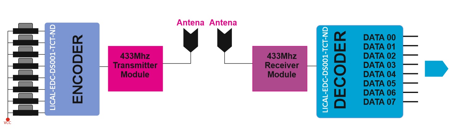
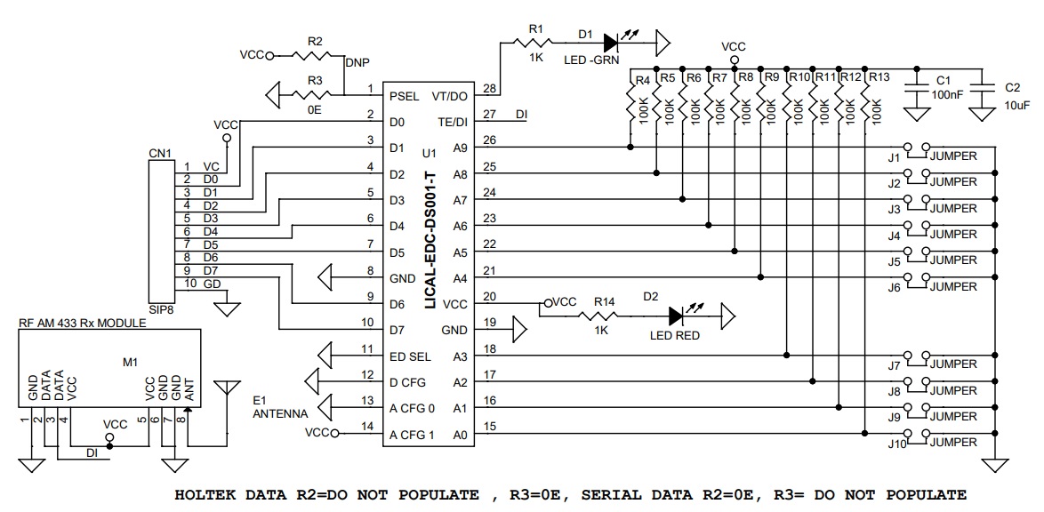
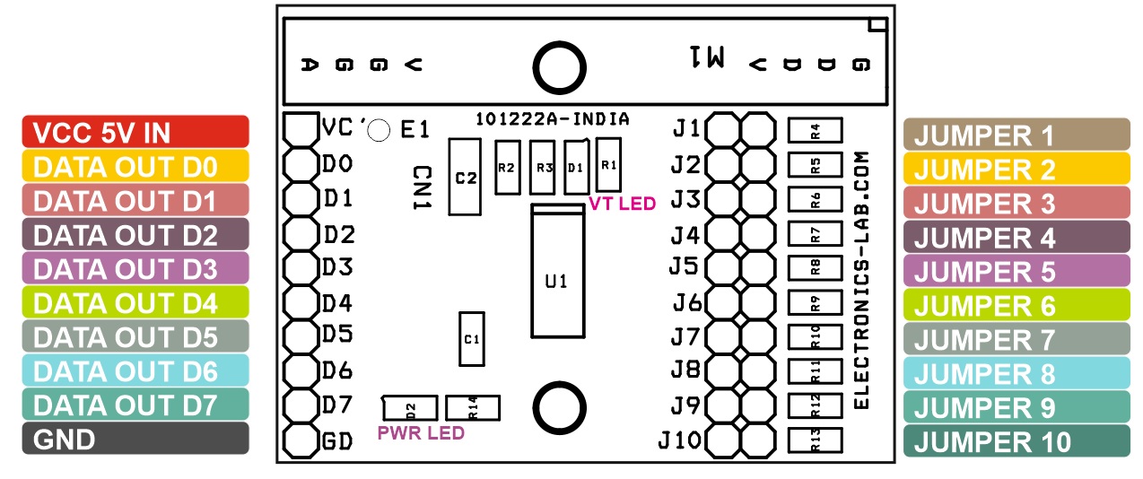
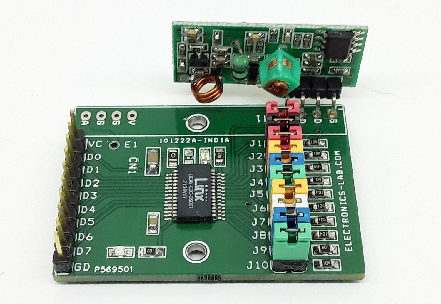
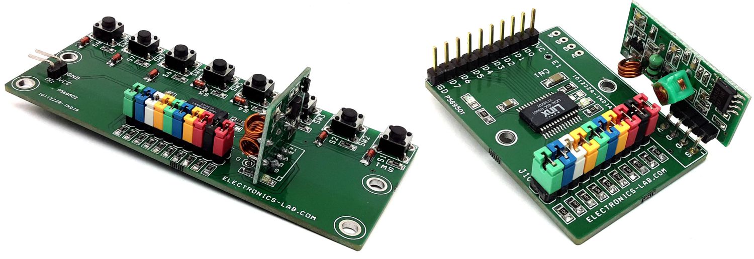
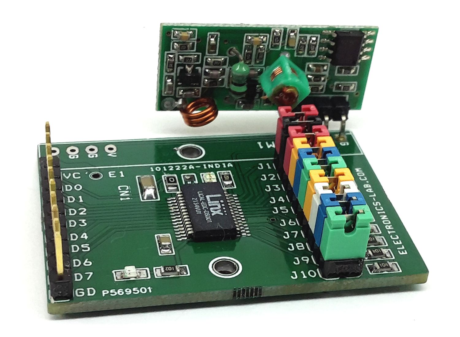
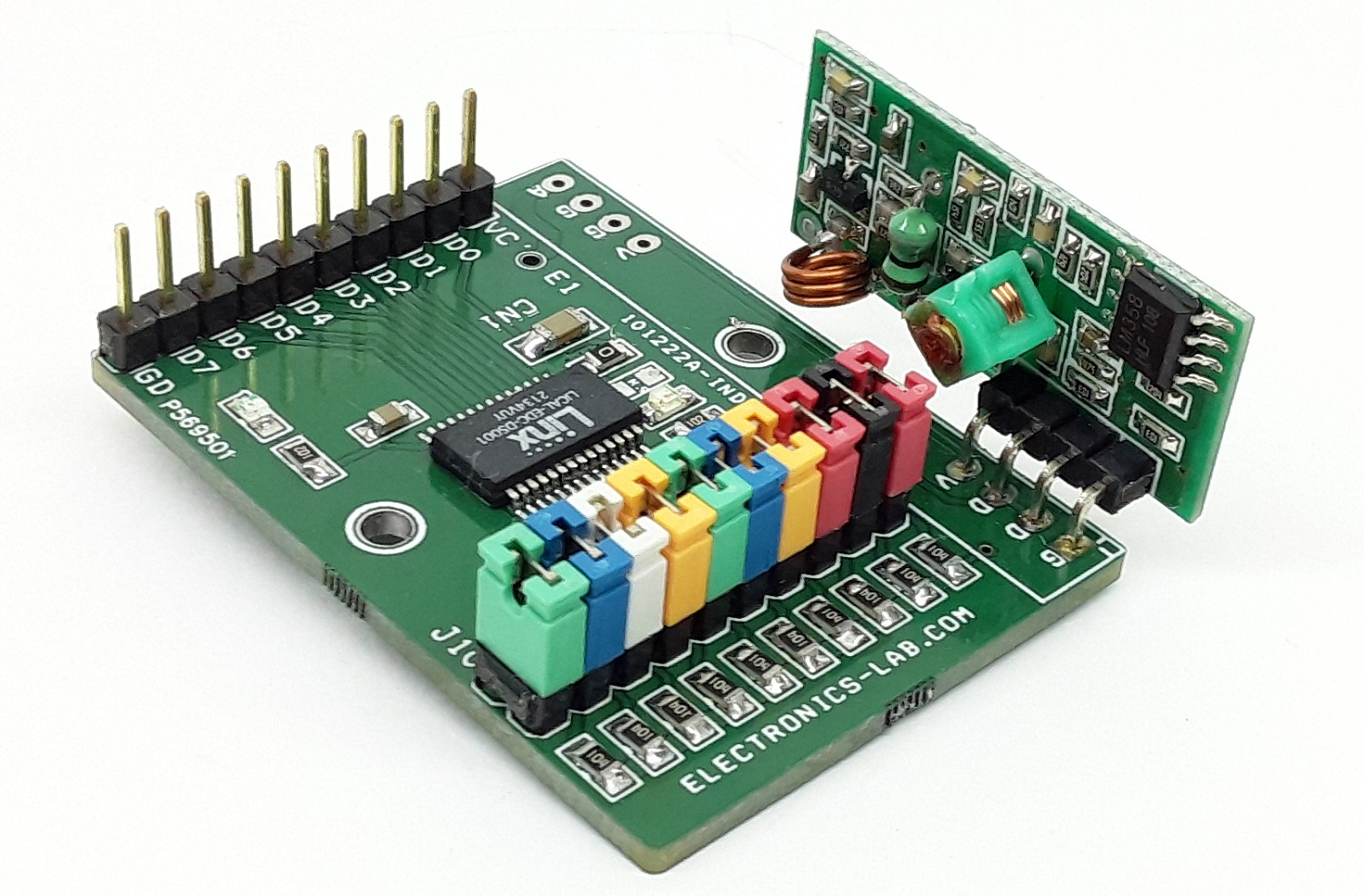
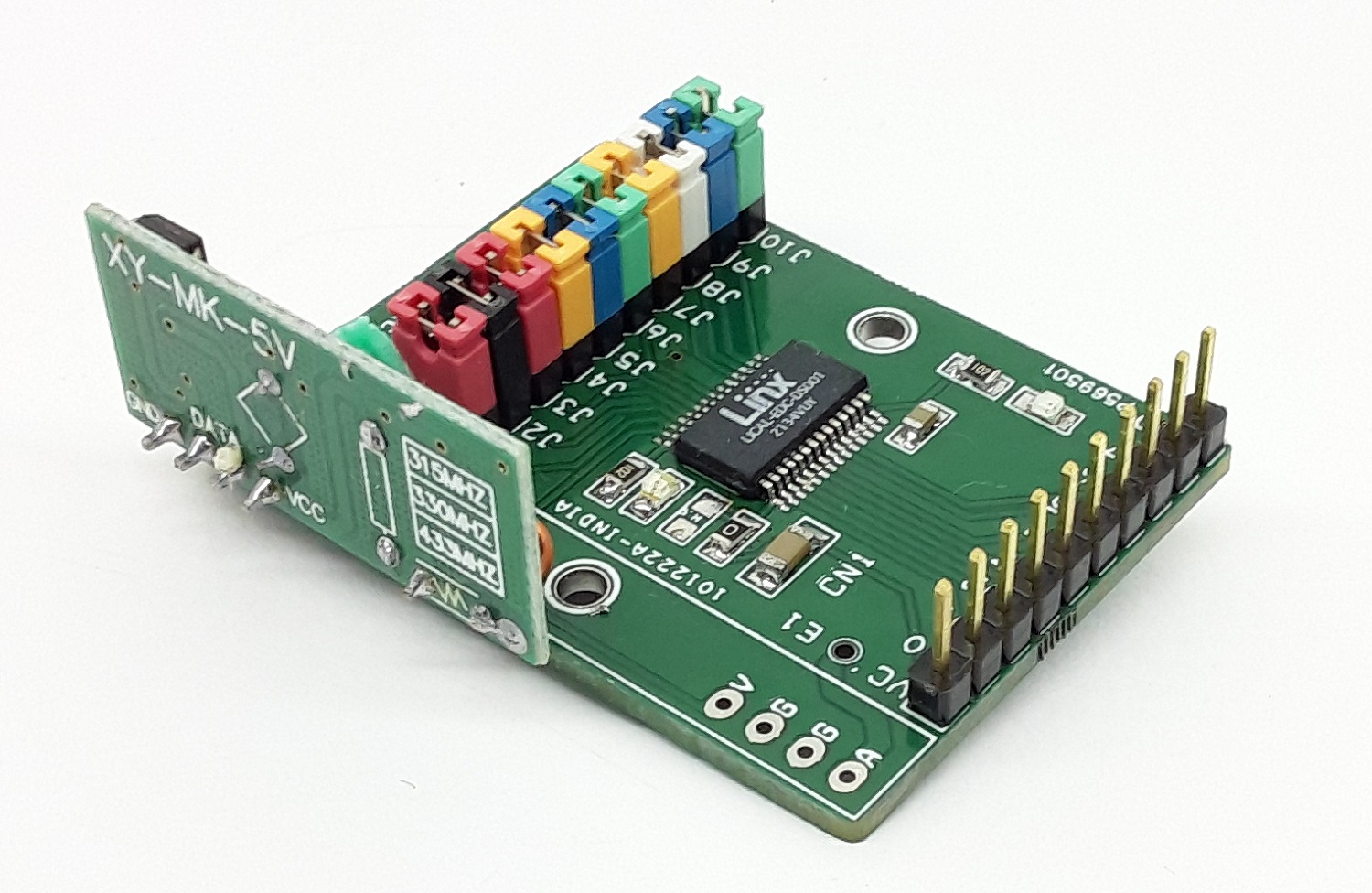
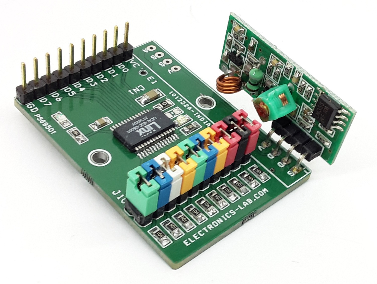
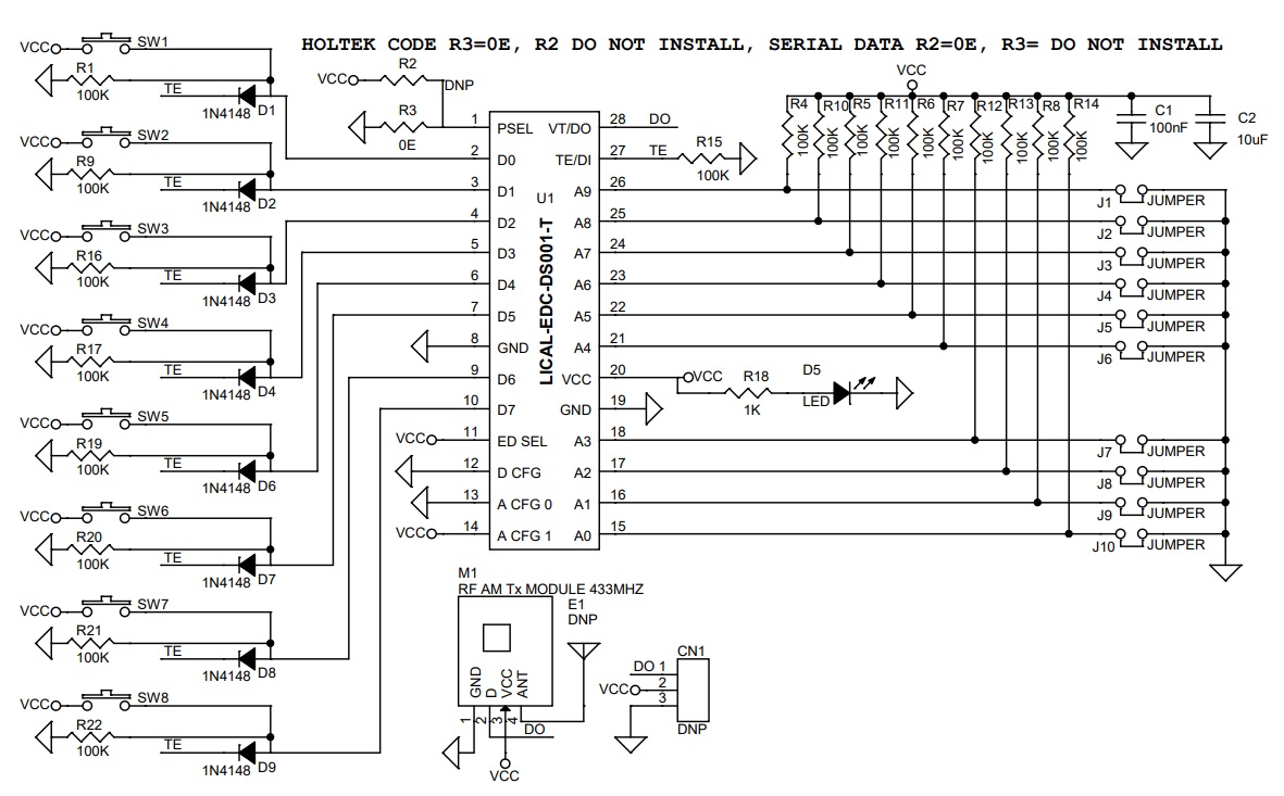
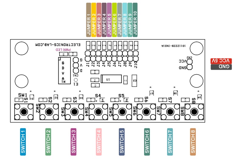
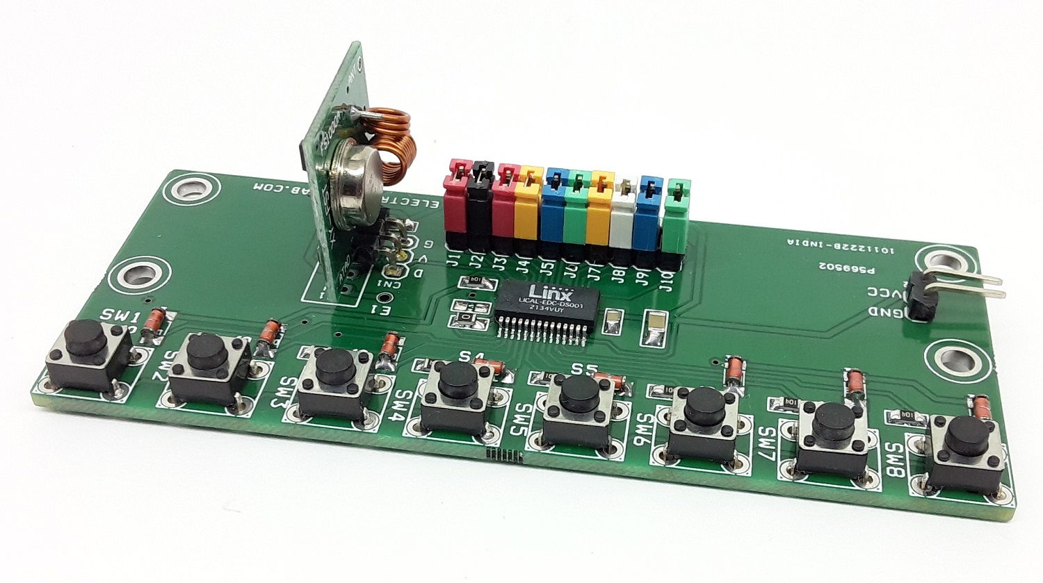
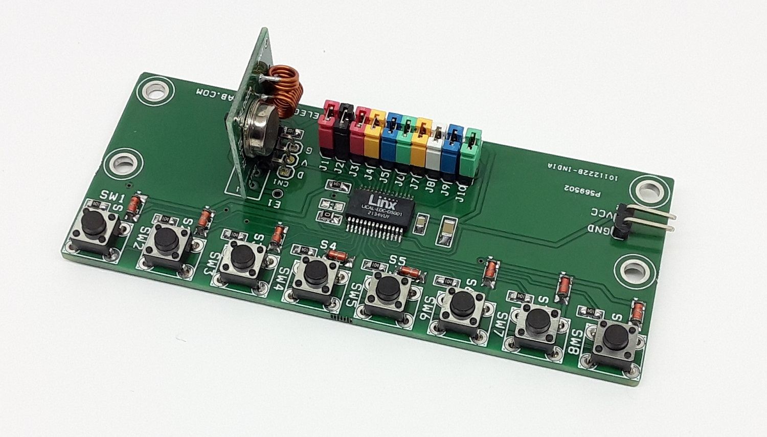
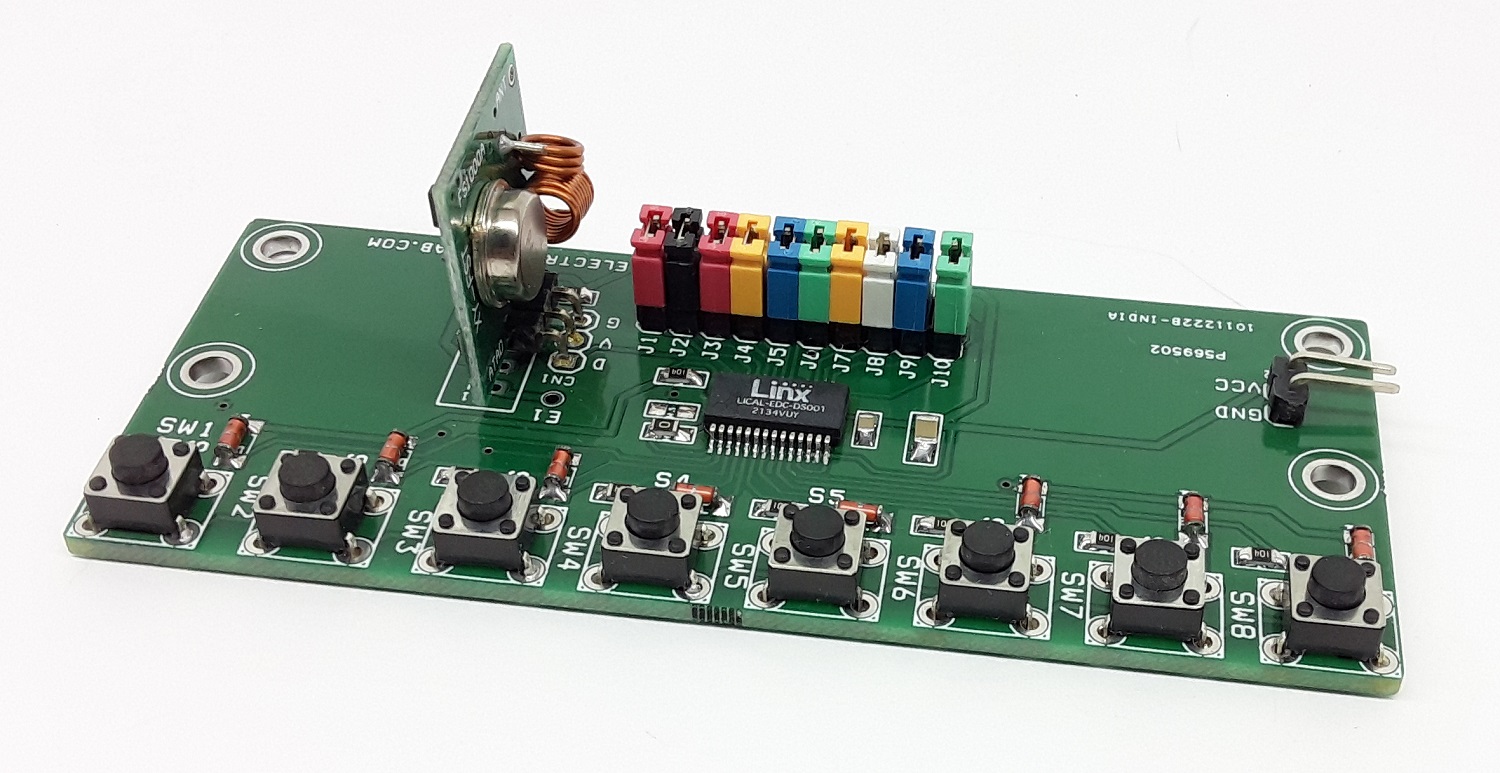
The project described here is 8 Channel RF Remote Receiver (Decoder). This 8-channel decoder is built using LICAL-EDC-DS001 chip from LINX. The board consists of the encoder/Decoder chip, 433Mhz RF Receiver module, and 10 x jumpers to set the address. Also, there is a header connector for data output which is ideal for controlling external devices, for example, relays. All outputs are compatible with TTL logic, normally they are low and go high when a valid signal is received and decoded by the chip. D2 onboard Power LED, D1 LED indicates valid transmission signal. All outputs are momentary (not latching)
10 Address Lines Selected through Jumpers J1 to J10
8 Data Output TTL Compatible Normally Low (Momentary)
On Board Power LED
On Board VT LED (Valid Transmission)
PCB Dimensions 45.09 x 33.02 mm
2 x 2.5mm Mounting Holes
System Configuration
A simple remote-control system consists of an encoder, an RF transmitter, an RF receiver, and a decoder. The encoder is connected to 8 buttons, The encoder detects the closure of one of the switches and converts that into a digital data stream. This data is then sent to an RF transmitter that conveys this data into free space. An RF receiver receives the data and sends it to a decoder. The decoder analyses the data and, if it is valid, replicates the switch closure on an output. This output is then connected to whatever circuitry is to be controlled. All outputs are momentary and TTL logic.
remote control system (transmitter and receiver)
This DS series decoder and encoder chip is ideal for remote control applications. It decodes the signal received by 433 MHz RF modules. When the DS enters Decoder Mode, it checks the state of the DIN line. If it is high, the P_SEL line is checked to set which protocol is used and the decoder receives the data. It compares the address in the received packet to its local address lines. If they match, the data is stored and a second packet is received. With the Holtek® protocol, the decoder compares the two packets. If they match, the received data bits are output on the data lines and the VT line is pulled high thus LED D1 is on. This protocol compares each packet with the previous one looking for a match. The serial protocol requires two matching packets for initial activation, then updates the lines on each subsequent packet. The DS then looks for the next packet on the DIN line. With the Holtek® protocol, once no valid data is received (there is a mismatch of address, data, or bit timings), the Data and VT lines are pulled low and the DS goes to sleep until DIN is pulled high. The Serial protocol holds the output states until a 130ms timer runs out. The Holtek® protocol compares two packets and, if they match, sets the outputs. If a data line is toggled during a transmission (D1 is activated while D0 is already active) then the received packet does not match the previous packet and the output lines are pulled low until the next packet arrives. This causes all of the outputs to briefly cut out when a line is toggled. The serial protocol uses a timer to prevent this cutout.
LICAL-EDC-DS001 Encoder/Decoder Chip
The same part can be used as an encoder or decoder by selecting the state of one pin. The DS Series also has two protocols built into the same part, selected by the state of a single pin. One is compatible with Holtek devices, such as the HT640 and HT658. The other protocol is a serial data structure that is much more immune to noise and edge jitter. This protocol offers much more range and reliability than the Holtek protocol while keeping the simple jumper addressing.
Theory of Operation
The DS Series is a remote-control encoder and decoder that offers two protocols in one part based on the state of the P_SEL line. The first protocol operates with the Holtek® HT640 encoder and HT658 decoder. The second is a serial protocol that offers more noise immunity and faster response time while keeping the simple addressing. The DS can operate as either an encoder or decoder based on the state of the E/D_SEL line. It does not operate as both simultaneously. When set as an encoder it monitors the state of the TE line. When the line is high the DS records the states of the data and address lines, assembles them into a packet, and outputs the packet three times. The data lines can be connected to switches or contacts. The address lines can be set with Jumpers. When set as a decoder the DS receives packets and validates them. The validation includes checking the bit timings and comparing the received address to the local address line settings. Two matching packets must be received consecutively. If the timings are good and the addresses match, the DS sets its data lines to match the received states. These lines can be connected to the application circuitry to be controlled. When the TE/DIN line is low, the DS goes into a low-power sleep mode.
Setting the Address
The project has ten address lines. This allows the formation of up to 1,022 (210 – 2) unique transmitter-receiver relationships, Jumper J1 to J10 can be used to set the address, all lines are pulled high. The chip rejects packets with addresses set to all high or all low. At least one address line must be different from the rest. The encoder does transmit all addresses, but the decoder rejects packets with all address lines set the same. The receiver’s address line states must match the transmitter’s exactly for a transmission to be recognized. If the addresses do not match, then the decoder takes no action.
Initial Operation
On power-up, the E/D_SEL line is tested to determine if the DS operates as an encoder or a decoder. If the line is high, the DS enters Encoder Mode. If low, it enters Decoder Mode. This is checked once on power-up. Once the operating mode is selected, the data-line direction is set. In either mode, a rising edge on the TE/DIN line wakes the device from low-power sleep.
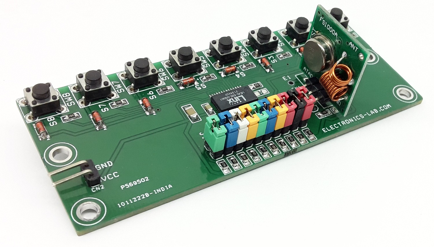
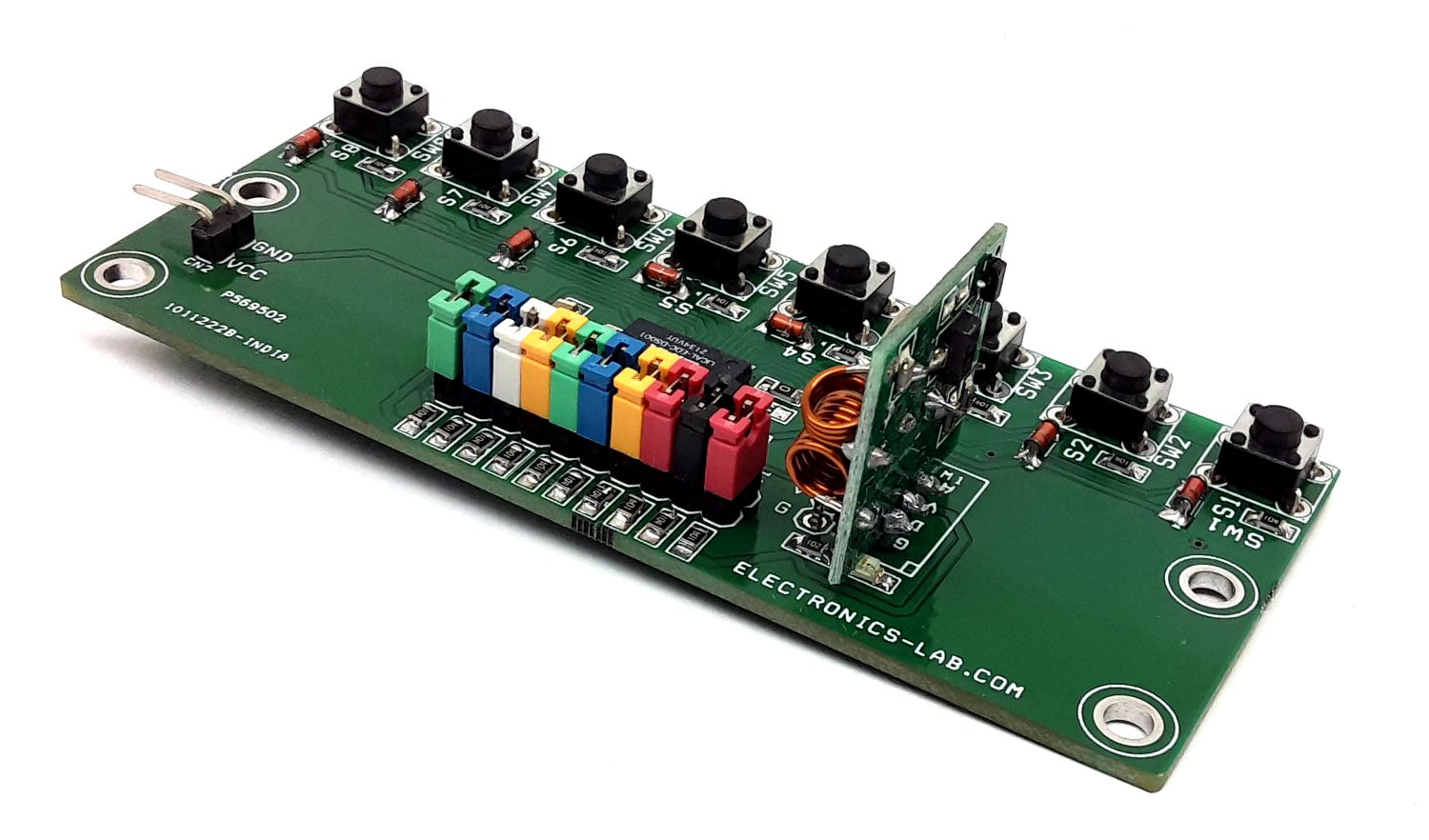
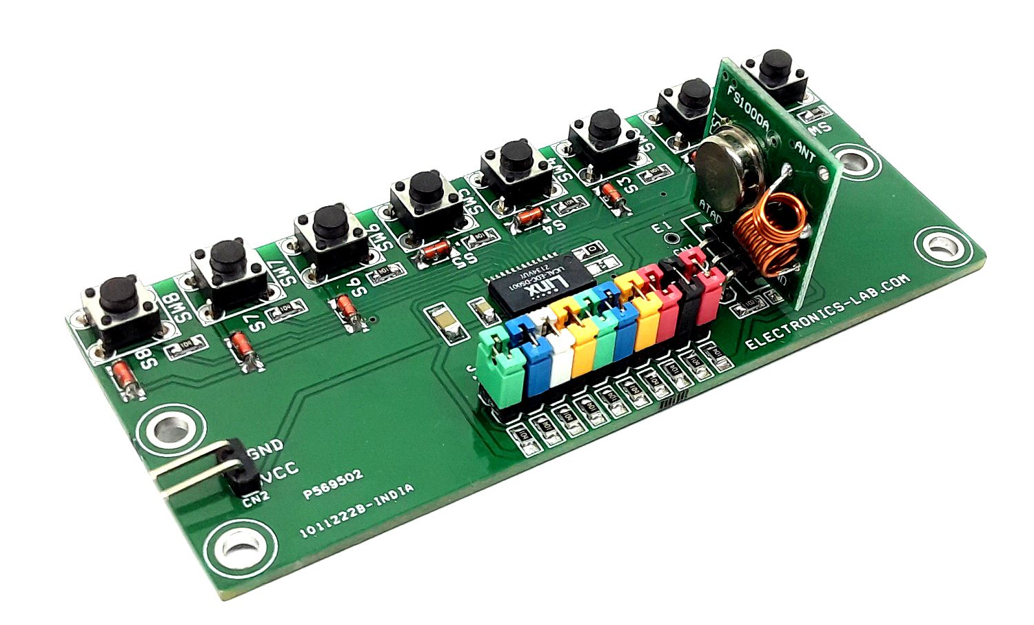
The project described here is an 8 Channel RF remote transmitter This transmitter is built using LICAL-EDC-DS001 chip from LINX. The project consists of the Encoder/Decoder chip, a 433Mhz RF module as a wireless link, 8 x tactile switches for operations, 10 x jumpers to set the transmitter address. This DS series decoder/encoder chip is ideal for remote control applications. It is able to transmit the status of up to 8 buttons across a wireless link. Addressing is accomplished by the logic state of 10 Jumpers J1 to J10.
The same part can be used as an encoder or decoder by setting the state of one pin. The DS Series also has two protocols built into the same part, selected by the state of a single pin. One is compatible with Holtek devices, such as the HT640 and HT658. The other protocol is a serial data structure that is much more immune to noise and edge jitter. This protocol offers much more range and reliability than the Holtek protocol while keeping the simple jumper addressing.
Theory of Operation
The DS Series is a remote-control encoder and decoder that offers two protocols in one part based on the state of the P_SEL line. The first protocol operates with the Holtek® HT640 encoder and HT658 decoder. The second is a serial protocol that offers more noise immunity and faster response time while keeping the simple addressing. The DS can operate as either an encoder or decoder based on the state of the E/D_SEL line. It does not operate as both simultaneously. When set as an encoder it monitors the state of the TE line. When the line is high the DS records the states of the data and address lines, assembles them into a packet, and outputs the packet three times. The data lines can be connected to switches or contacts. The address lines can be set with DIP switches or cut traces on a PCB. When set as a decoder the DS receives packets and validates them. The validation includes checking the bit timings and comparing the received address to the local address line settings. Two matching packets must be received consecutively. If the timings are good and the addresses match, the DS sets its data lines to match the received states. These lines can be connected to the application circuitry to be controlled. When the TE/DIN line is low, the DS goes into a low-power sleep mode.
remote control system (transmitter and receiver)
Setting the Address
The project has ten address lines. This allows the formation of up to 1,022 (210 – 2) unique transmitter-receiver relationships, Jumper J1 to J10 can be used to set the address, all lines are pulled high. The chip rejects packets with addresses set to all high or all low. At least one address line must be different from the rest. The encoder does transmit all addresses, but the decoder rejects packets with all address lines set the same. The receiver’s address line states must match the transmitter’s exactly for a transmission to be recognized. If the addresses do not match, then the decoder takes no action.
Initial Operation
On power-up, the E/D_SEL line is tested to determine if the DS operates as an encoder or a decoder. If the line is high, the DS enters Encoder Mode. If low, it enters Decoder Mode. This is checked once on power-up. Once the operating mode is selected, the data-line direction is set. In either mode, a rising edge on the TE/DIN line wakes the device from low-power sleep.
Encoder Mode
Once the chip enters Encoder Mode, it tests the state of the TE line. If it is high, the P_SEL line is checked to determine which protocol to use. Then the encoder records the states of the Data and Address lines and assembles a packet. When the Holtek® protocol is selected, the DS outputs the packet on the DOUT line three times. With the Serial protocol, it sends two packets, checking the states of the data lines each time. The second packet is the logical inversion of the first packet, ensuring a 50% duty cycle, which is an advantage for FCC testing. The DS then checks the state of the TE line again. It repeats this process for as long as the TE line is high. Once it goes low, the DS goes to sleep until TE is pulled high.
Decoder Mode
When the DS enters Decoder Mode, it checks the state of the DIN line. If it is high, the P_SEL line is checked to set which protocol is used and the decoder receives the data. It compares the address in the received packet to its local address lines. If they match, the data is stored and a second packet is received. With the Holtek® protocol, the decoder compares the two packets. If they match, the received data bits are output on the data lines and the VT line is pulled high. This protocol compares each packet with the previous one looking for a match. The serial protocol requires two matching packets for initial activation, then updates the lines on each subsequent packet. The DS then looks for the next packet on the DIN line. With the Holtek® protocol, once no valid data is received (there is a mismatch of address, data, or bit timings), the Data and VT lines are pulled low and the DS goes to sleep until DIN is pulled high. The Serial protocol holds the output states until a 130ms timer runs out. The Holtek® protocol compares two packets and, if they match, sets the outputs. If a data line is toggled during a transmission (D1 is activated while D0 is already active) then the received packet does not match the previous packet and the output lines are pulled low until the next packet arrives. This causes all of the outputs to briefly cut out when a line is toggled. The serial protocol uses a timer to prevent this cutout.
Note: The transmitter part is published here. The receiver part with multiple options will be published in the near future. The transmitter also can be used with Arduino + 433Mhz RF receiver module. Refer to the datasheet of the chip for more information about decoding the signal.
Connections and Other Information
Sw1 to Sw8 = Function Switches
CN2= PIN 1 = VCC 5V DC, PIN 2 = GND
Jumper J1 to J10 = For Address Configuration (should be the same for Transmitter and Receiver)
D5 Power LED
Transmitter PCB can accommodate 2 Types of RF Modules: 3 Pins CN1 or M1 4 Pin Module.
For Serial Protocol R2 = 0 Ohms, R3 Omit, For Holtek Protocol R3= 0 Ohms and R2 Omit (Read the datasheet of the chip for Serial/Holtek Protocol)
Features
Supply 5V DC
10 Address Lines Selected through Jumpers J1 to J10