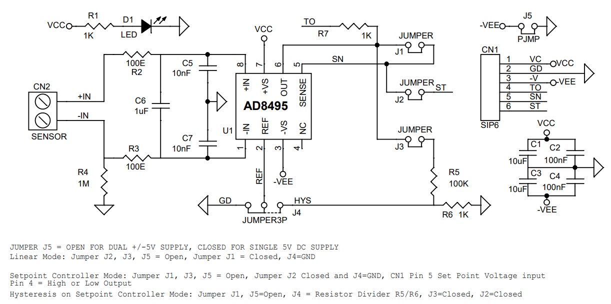
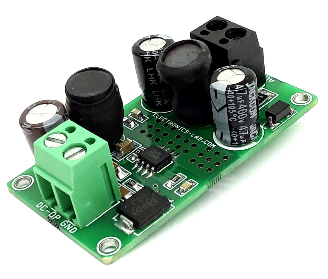
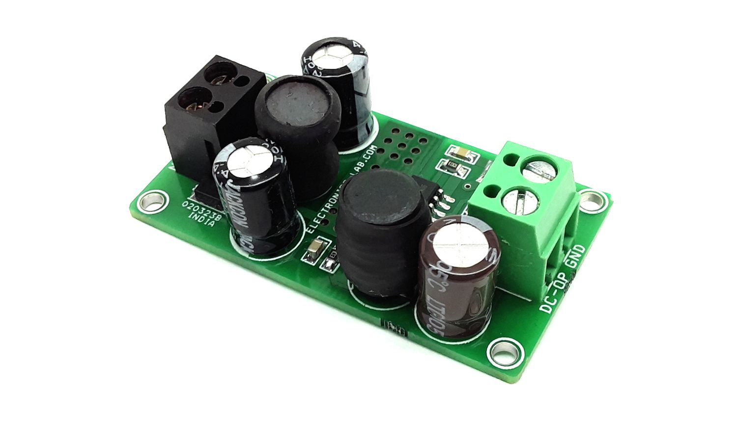
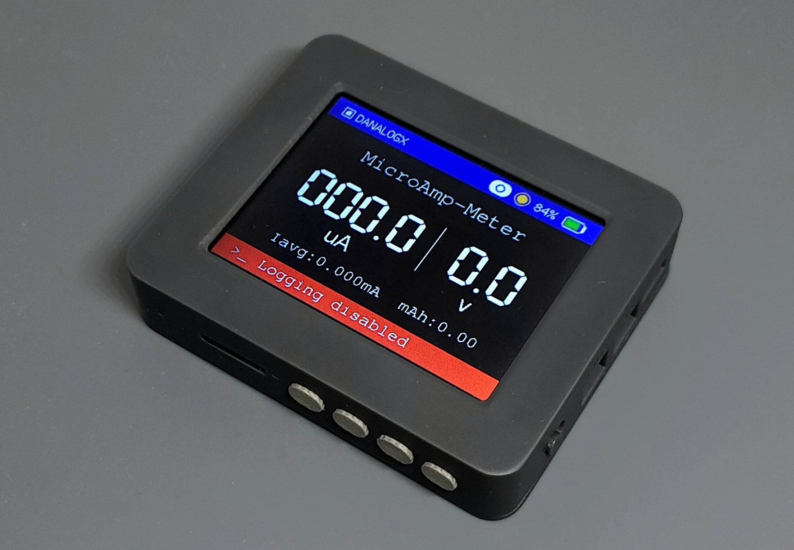
Danalogx’s Microamp-Meter- High-speed Wi-fi Current Meter and Micro SD card Logger – A Review

MicroAmp-Meter

The DanalogX MicroAmp-Meter is a device that functions as a high-speed Wi-Fi current profiler and Micro SD card logger. The MicroAmp-Meter is a highly efficient portable current meter that can quickly measure and plot the current consumption of embedded devices. It is an excellent tool, and with its automatic shunt-switching mechanism, it is able to measure current levels from 1uA to 1Amp.

Advantages of MicroAmp-Meter

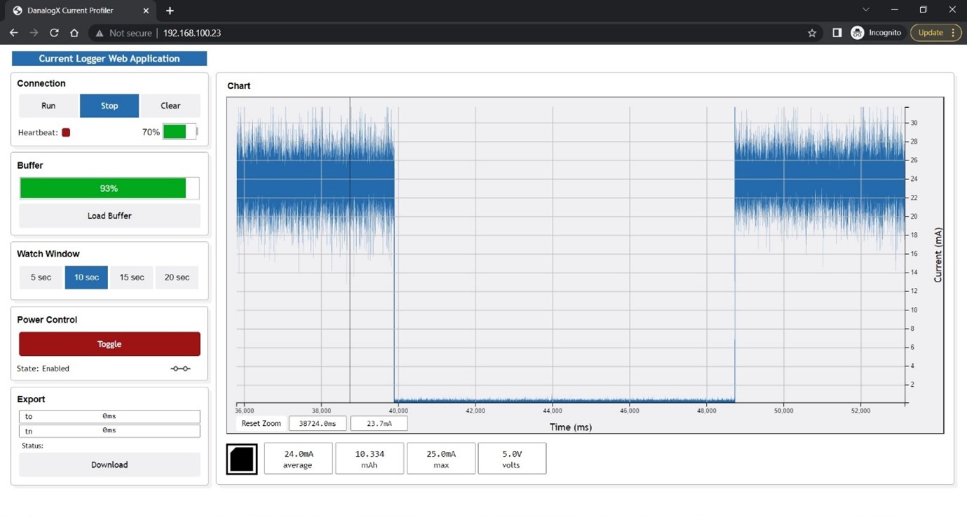
The MicroAmp-Meter is a great device with built-in Wi-Fi that displays the current consumption of the load in a web browser interface, including real-time graphical representation. The bi-directional Wi-Fi communication and remote power cycle control are some of its impressive features. It is an ideal tool for displaying current waveforms over time, similar to an oscilloscope over Wi-Fi. It also comes with a micro SD card slot and logging capability. This device is ideal for field testing as it allows you to measure the current profile over a long period, logging several parameters for over 12 hours. It is incredibly compact and portable, making it easy to carry. Ideally, it has a battery life of over 12 hours!

The MicroAmp-Meter is a reliable device with an automatic shunt-switching mechanism that precisely measures electrical current within the microamps to amps range. This wide range makes accurate and precise current measurements for embedded devices possible. The MicroAmp-Meter boasts a high ADC sampling rate and a core that runs at 80MHz. This device effectively captures noise and other short events by measuring current and voltage 4000 times per second. Its maximum voltage drop of 35 mV across all shunt ranges guarantees the accurate functioning of devices under test.

Wi-Fi-based current monitoring is an excellent approach to simplify the testing process! You can easily monitor the current performance of your device using just your mobile phone, tablet, or PC without the hassle of USB cables. This feature lets you conveniently manage your device from a distance, making it ideal for Hardware-in-the-loop testing.  This great tool empowers us to test devices anytime and anywhere. The MicroAmp-Meter is an ideal pick for students and hobbyists on a budget due to its affordability.

The hardware overvoltage protection circuit clamps the input to the ADC’s range. Due to their minimal forward voltage drop, Schottky diodes are utilized. The 3.3 V system rail that can sink current and the ground are connected to the Schottky diodes. The series resistor that comes after the Schottky diodes also aids in controlling the current flowing into the ADC. Additionally, there are indicators for measured voltage over range on LCD and Buzzer.

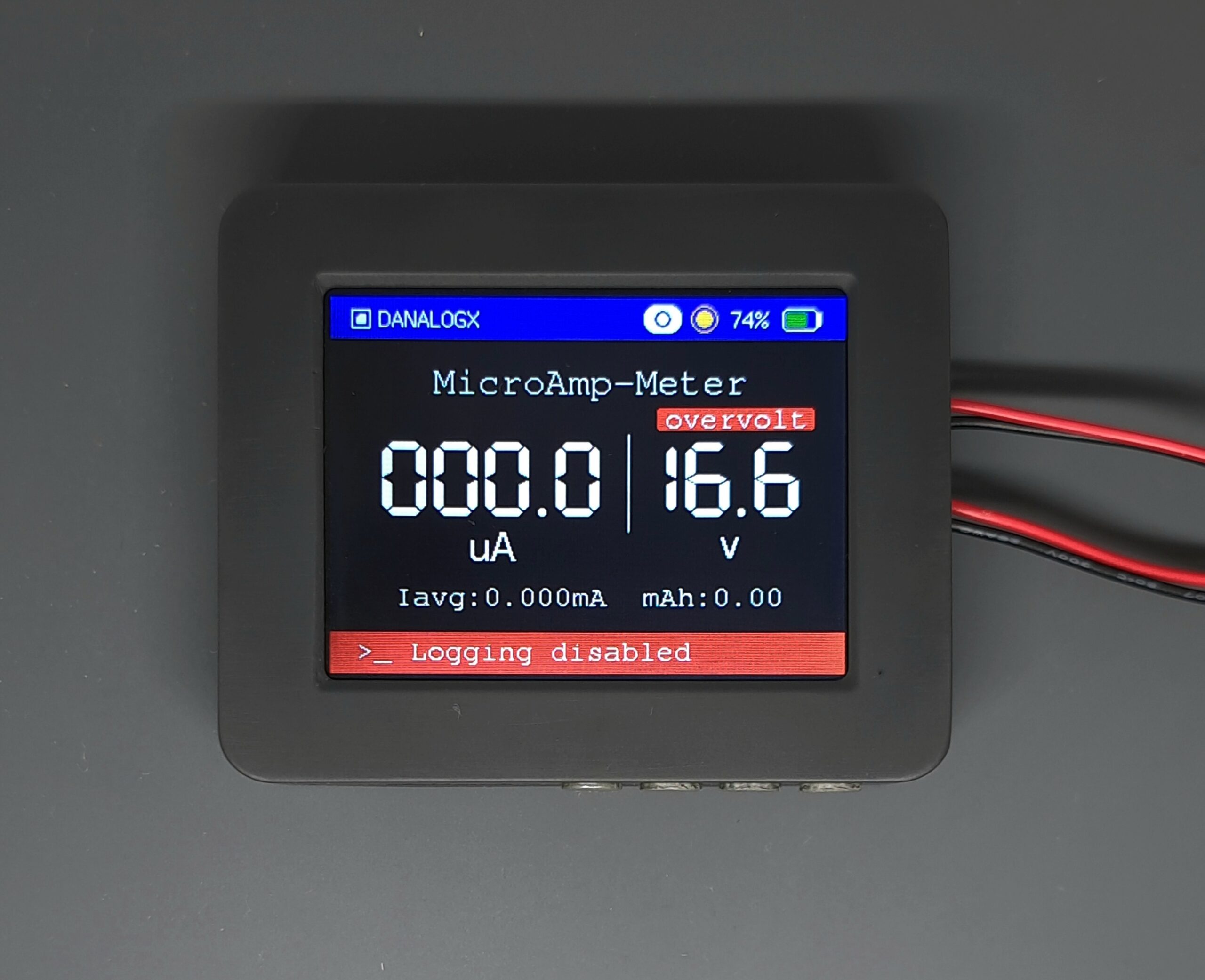
The overcurrent protection is handled by software. MicroAmp-Meter automatically turns off output if the current exceeds 1000mA. This feature is implemented with the highest software priority to execute the routine in less than 150us.
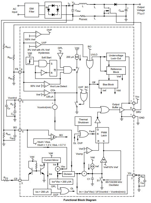
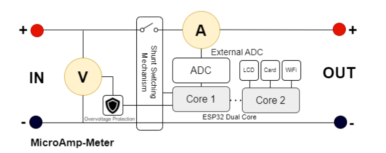
Block Diagram


Specifications

  • Processor- Dual core ESP32  at 80Mhz. Built-in Websocket server application
    – Each core is pinned to a separate task in RTOS.
    -The primary core of ESP32 reads analog data from external ADC, calculating current and switching shunts accordingly.
    -The secondary core handles LCD, voltage, battery SOC, micro SD card, and Wi-Fi functionalities.
  • Power- 1.8-12V up to 1000 mA
  • Filter- Hardware low pass filter
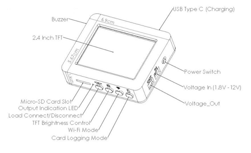
    – Software butterworth filter
  • Display – 2.4 inch TFT
  • Battery- 1500 mAh LiPo battery
    – Fast charging rate up to 0.6c. Battery charging time is less than two hours.
    – MAX17048G fuel gauge to detect battery SOC.
  • Three shunt stages:
    0-1000 uA
    1-300 mA
    300-1000 mA
  • Low burden voltage (max 30mV)
    Range 1: 30 µV/µA
    Range 2:100 µV/mA
    Range 3: 30 µV/mA
  • Ultrafast shunt switching in less than 200 microseconds.
  • Others-
    -Output control button.
    -TFT brightness control button.
    -Button for SD card logging
    -Button for turning on WIFI
  • Button for LCD brightness adjustment. Save power during SD card logging mode. LCD has 3 brightness levels.
    – Level 0 – Backlight completely turned OFF
    – Level 1 – Backlight intensity 50%
    – Level 2 – Backlight intensity 100%
  • Buffer for voltage over range indication, overload indication, and low battery indication.
  • Dimension- 5.67 cm x 6.9cm

Parameters

  • Current reading (Noise is filtered, and the reading is smoothed out using a Butterworth filter on this parameter)
  • Voltage reading
  • Average current value (T-1 and T time interval). This parameter shows raw current data over 1 second.
  • Current peak value
  • mAh (milliampere-hour). It is the standard for determining a battery’s energy capability. The parameter is highly helpful for determining the DUT battery timing calculation.

The website for this product includes an easy-to-follow guide for starting with the device.

Purchase Information

The Kickstarter page states a $100 or more Pledge to get a MicroAmp-Meter (including 2 x JST Cable). Pledge of $125 or more for MicroAmp-Meter with Micro SD Card/MicroAmp-Meter with Power Adapter. Pledge $150 or more for a complete MicroAmp-Meter Starter Kit. The estimated time of delivery is around Sep 2023.

Sound to RC Servo Driver v2.0 – Arduino Compatible

The project presented here is made for applications such as Animatronics, Puppeteer, sound-responsive toys, and robotics. The Arduino compatible board consists of LM358 OPAMP, ATMEGA328 microcontroller, microphone, and other components. The project moves the RC servo once receives any kind of sound.  The rotation angle depends on the sound level, the higher the sound level the bigger the movement, in other words, the movement of the servo is proportional to the sound level. The microphone picks up the soundwave and converts it to an electrical signal, this signal is amplified by LM358 op-amp-based dual-stage amplifier, D1 helps to rectify the sinewave into DC, and C8 works as a filter capacitor that smooths the DC voltage. ATmega328 microcontroller converts this DC voltage into a suitable RC PWM signal.

The project is Arduino compatible and an onboard connector is provided for the boot-loader and Arduino IDE programming. Arduino code is available as a download, and Atmega328 chips must be programmed with a bootloader before uploading the code. Users may modify the code as per requirement. More information on burning the bootloader is here: https://www.arduino.cc/en/Tutorial/BuiltInExamples/ArduinoToBreadboard

Direct Audio Input: The audio input signal should not exceed 5V, It is important to maintain the input audio signal at this maximum level, otherwise it can damage the ADC of ATMEGA328.

Features

  • Supply 5V to 6V DC (Battery Power Advisable)
  • RC Servo Movement 180 Degrees with Loud sound
  • Direct Sound Input Facility Using 3.5MM RC Jack
  • On Board Jumper Selection for Micro-Phone Audio or External Audio Signal
  • On Board Trimmer Potentiometer to Adjust the Signal Sensitivity
  • Flexible Operation, Parameters Can be Changed using Arduino Code
  • PCB Dimensions 44.45 x 36.20 mm

Connections and Other Details

  • CN1 Arduino Programming and Boot-Load Connector: Pin 1 = TX, Pin 2 = RX, Pin 3 = Reset, Pin 4 = GND, Pin 5 = VCC 5V DC, Pin 6 = D11, Pin 7 = D12, Pin 8 = D13
  • CN2 Direct Audio Input: Optional, Pin 1 Audio from External Speaker, Pin 2 = GND
  • CN3 Stereo EP 3.5MM Female Connector for External Audio Signal Input from Speaker
  • CN4 DC Input: Pin 1 VDD 5V to 6V DC, Pin 2 GND
  • CN5: No USE – Optional
  • CN6: RC Servo
  • Jumper J1: Input Signal Source Selection (External Audio Signal or Microphone)
  • PR1 Trimmer Potentiometer: Audio Signal Level Adjust
  • MK1: Condenser Microphone

Arduino Programming

Schematic

Parts List

NOQNTY.REF.DESC.MANUFACTURERSUPPLIER SUPPLIER PART NO
11CN18 PIN MALE HEADER PITCH 2.54MMWURTHDIGIKEY732-5321-ND
21CN22 PIN MALE HEADER PITCH 2.54MMWURTHDIGIKEY732-5315-ND
31CN3STEREO SOCKET 3.5MM FEMALECUI DEVICESDIGIKEYCP1-3525N-ND
41CN42 PIN SCREW TERMINAL PITCH 5.08MMPHOENIXDIGIKEY277-1247-ND
51CN53 PIN MALE HEADER PITCH 2.54MM WURTHDIGIKEY732-5316-ND
61CN63 PIN MALE HEADER PITCH 2.54MM WURTHDIGIKEY732-5316-ND
71C110uF/10V CERAMIC SMD SIZE 0805MURATA/YAGEODIGIKEY
86C2,C3,C5,C12,C4,C6100nF/50V CERAMIC SMD SIZE 0805MURATA/YAGEODIGIKEY
91SHUNTSHUNT FOR JUMPERSULLINS CONNCTDIGIKEYS9001-ND
103U3,C7,R10DNP
111C810uF/50V SMD ELECTROLYTICWURTHDIGIKEY732-8451-1-ND
121C9470uF/16V SMD ELECTROLYTICELITEDIGIKEY4191-CEE1C471MCB08A5CT-ND
132C10,C1122PF/50V SMD SIZE 0805MURATA/YAGEODIGIKEY
142D1,D21N4148 SMDONSEMIDIGIKEYFDLL4148CT-ND
151D3LED RED SMD SIZE 0805LITE ON INCDIGIKEY160-1427-1-ND
161J13 PIN MALE HEADER PITCH 2.54MM WURTHDIGIKEY732-5316-ND
171MK1CONDENSOR MICEPUI AUDIODIGIKEY668-1484-ND
186R1,R2,R5,R6,R7,R1110K 5% SMD SIZE 0805MURATA/YAGEODIGIKEY
193R3,R4,R131K 5% SMD SIZE 0805MURATA/YAGEODIGIKEY
201R824K 5% SMD SIZE 0805MURATA/YAGEODIGIKEY
211R91E 5% SMD SIZE 0805MURATA/YAGEODIGIKEY
221R12 1M 5% SMD SIZE 0805MURATA/YAGEODIGIKEY
231U1LM358 SMD SOIC8TIDIGIKEY296-LM358DRCT-ND
241U2ATMEGA328TQPF-32MICROCHIPDIGIKEYATMEGA328PB-AURCT-ND
251X116MhzECS INCDIGIKEYX1103-ND
261PR110K TRIMMER POTKYOCERADIGIKEY478-601030-ND

Connections

Gerber View

Code

/*
 Controlling a servo position using a potentiometer (variable resistor)
 by Michal Rinott <http://people.interaction-ivrea.it/m.rinott>

 modified on 8 Nov 2013
 by Scott Fitzgerald
 http://www.arduino.cc/en/Tutorial/Knob
*/
  
#include <Servo.h>

Servo myservo;  // create servo object to control a servo

int potpin = A2;  // analog pin used to connect the potentiometer
int val;    // variable to read the value from the analog pin

void setup() {
  myservo.attach(9);  // attaches the servo on pin 9 to the servo object
}

void loop() {
  val = analogRead(potpin);            // reads the value of the potentiometer (value between 0 and 60)
  val = map(val, 0, 60, 0, 180);     // scale it for use with the servo (value between 0 and 180)
  myservo.write(val);                  // sets the servo position according to the scaled value
  delay(15);                           // waits for the servo to get there
}


Photos


Video


Atmega328 Datasheet

Continuous Conduction Mode Pre-Converters Module for Power Factor Controller

This compact module shown here is a Continuous Conduction Mode (CCM) Power Factor Correction Step up Pre-Converter. All-important inputs and output pins are broken out for use in your application, making this board hackable! Please refer to the datasheet of the NCP1654 chip for easy alteration and configuration of the board as per requirements. This board controls the power switch conduction time (PWM) in fixed frequency mode and is dependent on the instantaneous coil current. This module drastically simplifies the PFC implementation scheme. It also integrates high safety features that make the NCP1654 module ideal for robust and compact PFC stages like an effective input power runaway clamping circuit. Please refer to the application schematic to create a powerful PFC using this pre-driver module. The chip is available with various options for frequency such as 65Khz, 133Khz, and 200Khz. Choose the appropriate chip as per frequency requirement This project is tested with a 65Khz oscillator chip.

Features

  • Supply 15V DC
  • ±1.5 A Totem Pole Gate Drive, can drive TO247 and TO220 MOSFETS
  • Average Current Continuous Conduction Mode
  • Fast Transient Response
  • Very Few External Components
  • Very Low Startup Currents (< 75 uA)
  • Very Low Shutdown Currents (< 400 uA)
  • Low Operating Consumption
  • Accurate Fully Integrated 65
  • Latching PWM for cycle−by−cycle Duty−Cycle Control
  • Internally Trimmed Internal Reference
  • Undervoltage Lockout with Hysteresis
  • Soft−Start for Smoothly Startup Operation
  • Shutdown Function
  • PCB Dimensions 26.04 x 17.94mm

Safety Features

  • Inrush Current Detection
  • Overvoltage Protection
  • Undervoltage Detection for Open Loop Detection or Shutdown
  • Brown−Out Detection
  • Soft−Start
  • Accurate Overcurrent Limitation
  • Overpower Limitation

Connections Connector CN1

  • Pin 1 = VCC 15V DC, Pin 2 = GND, Pin 3 = BO Brown-Out/IN, Pin 4 = CS, Pin 5 = NC, Pin 6 = GND, Pin 7 = Output (MOSFET Gate), Pin 8 = VCC 15V DC, Pin 9 = NC, Pin 10 = FB/Feedback Voltage
  • D1 Power LED

VCC

This pin is the positive supply of the IC. The circuit typically starts to operate when VCC exceeds 10.5 V and turns off when VCC goes below 9 V. After start−up, the operating range is 9 V up to 20 V.

CS (Current Sense)

This pin sources a current ICS which is proportional to the inductor current IL. The sense current ICS is for overcurrent protection (OCP), overpower limitation (OPL) and PFC duty cycle modulation. When ICS goes above 200 uA, OCP is activated and the Drive Output is disabled.

BO (VBO) Brow-Out/In

BO pin detects a voltage signal proportional to the average input voltage. When VBO goes below VBOL, the circuit that detects too low input voltage conditions (brown−out), turns off the output driver and keeps it in low state until VBO exceeds VBOH. This signal which is proportional to the RMS input voltage Vac is also for overpower limitation (OPL) and PFC duty cycle modulation.

VFB (Voltage Feedback/Shutdown)

This pin receives a feedback signal VFB that is proportional to the PFC circuit’s output voltage. This information is used for both output regulation, overvoltage protection (OVP), and output Undervoltage protection (UVP) to protect the system from damage at feedback abnormal situations. When VFB goes above 105% VREF, OVP is activated and the Drive Output is disabled. When VFB goes below 8% VREF, the device enters a low−consumption shutdown mode.

OP (Drive Output)

The high current capability of the totem pole gate drive (±1.5 A) makes it suitable to effectively drive high gate charge power MOSFET

Schematic

Parts List

NO.QNTY.REF.DESC.MANUFACTURERSUPPLIERSUPPLIER'S PART NO
11CN110 PIN MALE HEADER RIGHT ANGLE PITCH 2.54MMWURTHDIGIKEY732-2670-ND
21C11KPF(1nF)/50V CERAMIC SMD SIZE 0805YAGEO/MURATADIGIKEY
31C2DNP
41C30.47uF/50V CERAMIC SMD SIZE 0805YAGEO/MURATADIGIKEY
51C42.2uF/50V CERAMIC SMD SIZE 0805YAGEO/MURATADIGIKEY
61C5220KF(0.22uF)/50V CERAMIC SMD SIZE 0805YAGEO/MURATADIGIKEY
71C610uF/25V CERAMIC SMD SIZE 1210 OR 1206YAGEO/MURATADIGIKEY
81C70.1uF/50V CERAMIC SMD SIZE 0805YAGEO/MURATADIGIKEY
91C810PF/50V CERAMIC SMD SIZE 0805YAGEO/MURATADIGIKEY
101D1LED RED SMD SIZE 0805OSRAMDIGIKEY475-1278-1-ND
112R1,R23.3M 5% SMD SIZE 0805YAGEO/MURATADIGIKEY
122R7,R80E SMD SIZE 1206YAGEO/MURATADIGIKEY
131R43.6K 1% SMD SIZE 0805YAGEO/MURATADIGIKEY
142R5,R61.8M 5% SMD SIZE 1206YAGEO/MURATADIGIKEY
151R91K 5% SMD SIZE 0805YAGEO/MURATADIGIKEY
161R1047K 5% SMD SIZE 0805YAGEO/MURATADIGIKEY
171R1122K 5% SMD SIZE 0805YAGEO/MURATADIGIKEY
181R1282K 1% SMD SIZE 0805YAGEO/MURATADIGIKEY
191R1312K 5% SMD SIZE 0805YAGEO/MURATADIGIKEY
201R141.2K 5% SMD SIZE 0805YAGEO/MURATADIGIKEY
211R15499E 1% SMD SIZE 0805YAGEO/MURATADIGIKEY
221U1NCP1654BD65R2GONSEMIDIGIKEYNCP1654BD65R2GOSCT-ND
231R30E SMD SIZE 0805YAGEO/MURATADIGIKEY

Connections

Block Diagram

Application Schematic

Functional Block Diagram

Gerber View

Photos

NCP1654 Datasheet

Precision Thermocouple Amplifiers with Cold Junction Compensation – Temperature Range −25°C to +400°C

This Thermocouple Amplifier project provides a simple, low-cost solution for measuring thermocouple temperature. This board simplifies many of the difficulties of measuring thermocouples output. An integrated temperature sensor performs cold junction compensation. A fixed-gain instrumentation amplifier amplifies the small thermocouple voltage to provide a 5 mV/°C output. The high common-mode rejection of the amplifier blocks common-mode noise that the long thermocouple leads can pick up. For additional protection, the high impedance inputs of the amplifier make it easy to add extra filtering. The module can be used as standalone thermometers or as switched output setpoint controllers using either a fixed or remote setpoint control. The module can be powered from a single-ended supply (less than 3V) and can measure temperatures below 0°C by offsetting the reference input. To minimize self-heating, an unloaded AD8495 typically operates with a total supply current of 180 μA, but it is also capable of delivering in excess of ±5 mA to a load. The board can be interfaced with K-type (chromel-alumel) thermocouples. With an operating single supply of 5V, the 5 mV/°C output allows the devices to cover nearly 1000 degrees of a thermocouple’s temperature range. The project can also work with 3V supplies, allowing them to interface directly with lower-supply ADCs. They can also work with supplies as large as 36V in industrial systems that require a wide common-mode input range. The AD8495 cold junction compensation is optimized for operation in a lab environment, where the ambient temperature is around 25°C. The AD8495 is specified for an ambient range of 0°C to 50°C.

Features

  • Supply Dual 5V DC (+/-5V DC)
  • Low cost and easy to use
  • Measurement Temperature Range −25°C to +400°C
  • ±2°C Accuracy Temperature Ranges
  • Pretrimmed for K-type thermocouples
  • Internal cold junction compensation
  • High-impedance differential input
  • Standalone 5 mV/°C thermometer
  • Reference pin allows offset adjustment
  • Mode: Linear, Set Point Controller, Hysteresis on Setpoint Controller, Selection Using Jumpers
  • Thermocouple break detection
  • On Board Power LED
  • 4 x 2.5mm Mounting Holes
  • PCB Dimensions 31.12 x 27.31mm

Applications

  • K-type thermocouple temperature measurement
  • Setpoint controller
  • Celsius thermometer
  • Universal cold junction compensator
  • White goods (oven, stove top) temperature measurements
  • Exhaust gas temperature sensing
  • Catalytic converter temperature sensing

The board is designed to allow users to quickly prototype the precision thermocouple amplifiers for various user-defined configurations for different applications. The circuit has three modes of operation: linear mode, setpoint controller mode, and hysteresis on setpoint controller mode. Various modes can be set using onboard jumpers.

Linear Mode: Jumper J2, J3, J5 = Open, Jumper J1 = Closed, J4=GND

The linear mode can be selected by closing Jumper J1 and J4 = GND linear, the output voltage of the AD8495 is calculated as follows:

VOUT = (T_MJ × 5 mV/°C) + VREF

where T_MJ is the thermocouple measurement junction temperature.

Setpoint Controller Mode: Jumper J1, J3, J5 = Open, Jumper J2 Closed and J4=GND, CN1 Pin 5 Set Point Voltage input, Pin 4 = High or Low Output

The board operates as a temperature setpoint controller when configured with either a thermocouple input from a remote location or with the AD8495 being used as a temperature sensor. When the measured temperature is below the setpoint temperature, the output voltage goes to −VS. When the measured temperature is above the setpoint temperature, the output voltage goes to +VCC. For optimal accuracy and common mode rejection ratio (CMRR) performance, the setpoint voltage must be created with a low-impedance source. If the setpoint voltage is generated with a voltage divider, a buffer is recommended.

Hysteresis on Setpoint Controller Mode: Jumper J1, J5=Open, J4 = Resistor Divider R5/R6, J3=Closed, J2=Closed  

Hysteresis can be added to the setpoint controller by using a resistor R5, R6 divider from the output to the reference pin, The resistors installed on the board are 1 kΩ and 100 kΩ, which creates a window of approximately 10°C around the setpoint temperature for a +VCC of 5 V.

Measuring Negative Temperatures

The board can measure negative temperatures using either single or dual supplies. When operating on dual supplies with the J4 jumper = GND   position (reference pin grounded), a negative output voltage indicates a negative temperature at the thermocouple measurement junction. When operating the board series evaluation board on a single supply level, apply a positive voltage (less than +VS) on the reference pin to shift the output. The jumper from J2 must be removed so that the reference pin is not grounded. An output voltage less than VREF indicates a negative temperature at the thermocouple measurement junction.

Thermocouple Break Detection

The board offers open thermocouple detection. The inputs of the AD8495 are PNP type transistors, which means that the bias current always flows out of the inputs. Therefore, the input bias current drives any unconnected input high, which rails the output. Resistor R4 connected to GND causes the AD8495 output to rail high in an open thermocouple condition.

Gain Error

Gain error is the amount of additional error when measuring away from the measurement junction calibration point. For example, if the part is calibrated at 25°C and the measurement junction is 100°C with a gain error of 0.1%, the gain error contribution is (100°C − 25°C) × (0.1%) = 0.075°C. This error can be calibrated with a two-point calibration if needed, but it is usually small enough to ignore.

Ambient Temperature Rejection

The specified ambient temperature rejection represents the ability of the AD8495 to reject errors caused by changes in the ambient temperature/reference junction. For example, with 0.025°C/°C ambient temperature rejection, a 20°C change in the reference junction temperature adds less than 0.5°C error to the measurement.

Input Voltage Protection

The board has very robust inputs. Input voltages can be up to 25 V from the opposite supply rail. For example, with a +5 V positive supply and a −3 V negative supply, the board can safely withstand voltages at the inputs from −20 V to +22 V. Voltages at the reference and sense pins should not go beyond 0.3 V of the supply rails.

Connections and Other Details

  • CN1: Pin 1 = VCC +5V DC, Pin 2 = GND, Pin 3 = -VEE -5V, Pin 4 Temperature V-Output, Pin 5 = Sense (No Use), Pin 6 = Set Point V-Input
  • CN2: Pin 1 = K Type Sensor + Input, Pin 2 = Sensor -Input
  • Jumper J1: For Set the Linear Output
  • Jumper J2: For Set Point Input Mode
  • Jumper J3: For Hysteresis on Setpoint Controller Mode
  • Jumper J4: For Reference Ground or Hysteresis Selection
  • Jumper J5: Closed for Single Supply Input, Open for Dual Power Supply Input (Solder Jumper)

Schematic

Parts List

NO.QNTY.REF.DESC.MANUFACTURESUPPLIER SUPPLIER PART NO
11CN16 PIN MALE HEADER PITCH 2.54MMWURTHDIGIKEY732-5319-ND
21CN2TEMPERETURE SENSOR CONNECTORLABFACILITYELEMENT143810628
32C1,C310uF/16V CERAMIC SMD SIZE 0805YAGEO/MURATADIGIKEY
42C2,C4100nF/50V CERAMIC SMD SIZE 0805YAGEO/MURATADIGIKEY
52C5,C710nF/50V CERAMIC SMD SIZE 0805YAGEO/MURATADIGIKEY
61C61uF/25V CERAMIC SMD SIZE 0805YAGEO/MURATADIGIKEY
71D1LED RED SMD SIZE 0805OSRAMDIGIKEY75-1278-1-ND
83J1,J2,J3JUMPER- 2 PIN MALE HEADER PITCH 2.54MMWURTHDIGIKEY732-5315-ND
91J4JUMPER-3PIN MALE HEADER PITCH 2.54MMWURTHDIGIKEY732-5316-ND
101J5PJMP-PCB SOLDER JUMPER
113R1,R6,R71K 1% SMD SIZE 0805YAGEO/MURATADIGIKEY
122R2,R3100E 1% SMD SIZE 0805YAGEO/MURATADIGIKEY
131R41M 1% SMD SIZE 0805YAGEO/MURATADIGIKEY
141R5100K 1% SMD SIZE 0805YAGEO/MURATADIGIKEY
151U1AD8495 SOIC8ANALOG DEVICESDIGIKEYAD8495ARMZ-R7CT-ND
164SHUNTSHUNT-JUMPERSULLINS CONNCTDIGIKEYS9001-ND

Connections

Gerber View

Photos

Video


AD8495 Datasheet

Universal Input AC/DC Switching Buck Regulator – 85V -265V AC Input – 5V/150mA DC Output

The project presented here is a universal input AC/DC switching buck regulator with ultra-low standby power that is capable of delivering up to 2.5W output power. The RAA223012 chip is the heart of the project which combines constant off-time control for heavy load and Pulse Frequency Modulation (PFM) for light-load operation. Constant off-time controls switching frequency above the audible frequency of approximately 50kHz. PFM eliminates any potential audible noises while offering superior light-load efficiency and ultra-low power consumption (<10mW at no load). Efficiency is achieved up to 75%. The built-in frequency dithering further reduces the EMI noise spectrum.  The RAA223012 also features input brownout protection that prevents input circuitry from the overcurrent at low input voltage, and hiccup protections for output fault conditions such as short-circuit, overload, and open feedback.

Features

  • Universal Input 85V to 265V AC 50/60Hz
  • Output 5V DC, 150mA
  • Output Short Circuit Protection
  • Overload Protection (OLP)
  • Short-Circuit Protection (SCP)
  • Open Feedback Protection
  • Over-Temperature Protection (OTP)
  • 4 x 2.5mm Mounting Holes
  • PCB dimensions 52.07 x 28.58 mm

Connections And Other Details

  • CN1: Pin 1 = AC Live Input, Pin 2 = AC Neutral Input (85V to 265V AC Range)
  • CN2: Pin 1 = +5V DC Output, Pin 2 = GND
HIGH VOLTAGE: Dangerous voltage exists until the power is OFF. This power supply uses hazardous voltage. The PCB must be installed in an enclosure that prevents accidental contact. Use Plastic screws to mount the PCB. Wait for a few minutes after the input power is disconnected before touching the board. Make sure the bulk capacitor fully discharges.

Short-Circuit Protection

When the output is shorted, VOUT = 0, VFB drops to zero because of the feedback network, introducing a delay. Before VFB drops to VFB_TOFFMIN, the RAA223012 operates with TONMAX and TOFFMIN, which quickly builds up a high current (>IPK) because the inductor peak current does not get reset. When the current reaches ISC_TH, a timer is started. If the inductor current reaches ISC_TH for four consecutive cycles, the RAA223012 determines that a short-circuit is present and immediately shuts off the switching. The IC then quickly charges VCC up to 5.9V and discharges it with a 19µA current source to 3.4V. When VCC drops to 3.4V, a 1.6mA current source charges VCC back to 5.9V where the IC resumes switching.  When the RAA223012 resumes switching, assuming VFB drops to zero, the IC operates with the increased TOFFMIN_MAX so the inductor current can fully reset below the maximum peak limit. The RAA223012 operates in  CCM with the inductor peak current being limited at IPK, with an average current around 240mA during the short.  The part remains in hiccup mode until the short is removed. When the short is removed, VOUT returns to normal.

Schematic

Parts List

NOQNTYREF.DESCMANUFACTURERSUPPLIERSUPPLIER'S PART NO
11CN12 PIN SCREW TERMINAL PITCH 5.08MMPHOENIXDIGIKEY277-1247-ND
21CN22 PIN SCREW TERMINAL PITCH 5.08MMPHOENIXDIGIKEY277-1247-ND
31C10.22uF/25V CERAMIC SMD SIZE 1206YAGEO/MURATADIGIKEY
41C21uF/25V CERAMIC SMD SIZE 1206YAGEO/MURATADIGIKEY
51C3470PF/50V CERAMIC SMD SIZE 0805YAGEO/MURATADIGIKEY
62C4,C54.7uF/400VWURTHDIGIKEY732-8689-3-ND
71C6220uF/25VPANASONICDIGIKEYP10271-ND
81C70.47uF/25V CERAMIC SMD SIZE 0805YAGEO/MURATADIGIKEY
91D11N4148 SMDMICROCHIPDIGIKEY1N4148UR-1-ND
103D2,D3,D51N4007 SMDDIODE INC.DIGIKEYS1MBDITR-ND
111D4MURS360 SMDDIODE INC.DIGIKEY31-MURS360CT-ND
121L11mH 8X8MM SMD OR THTWURTHDIGIKEY732-3261-ND
131L2560uH 8X8MM SMD OR THTBOURNSDIGIKEYRLB0914-561KL-ND
141R10E SMD SIZE 0805YAGEO/MURATADIGIKEY
151R2120K 1% SMD SIZE 0805YAGEO/MURATADIGIKEY
161R34.7E OR 5.1E 2W 5% SMD 2512YAGEO/MURATADIGIKEY
171R4100K 1% SMD SIZE 0805YAGEO/MURATADIGIKEY
181R510K 1% SMD SIZE 0805YAGEO/MURATADIGIKEY
191U1RAA223012 SOIC8RENESASDIGIKEY20-RAA2230124GSP#HA0CT-ND

Connections

Gerber View

Photos

Video

RAA223012 Datasheet

Espressif Systems ESP32-H BLE & IEEE 802.15.4 Modules

Espressif Systems ESP32-H BLE and IEEE 802.15.4 Modules are powerful, generic BLUETOOTH® Low Energy and IEEE 802.15.4 combo modules featuring the ESP32-H2 chip. The ESP32-H is suitable for building IoT applications with high requirements for power consumption.

The Espressif ESP32-H module is small-sized and pin-to-pin compatible with the ESP32-C3-MINI and ESP32-C6-MINI modules.

Block Diagram

Features

  • 32-bit RISC-V single-core processor that operates at up to 96MHz
  • 19x programmable GPIOs, with support for UART, SPI, I2C, I2S, Remote Control Peripheral, LED PWM, Full-speed USB Serial/JTAG Controller, GDMA, and MCPWM
  • Can be used for building Thread end devices, as well as Thread border routers and Matter bridges by combining it and an ESP Wi-Fi SoC
  • 320KB SRAM, 128KB ROM, 4KB LP memory, and works with external flash

Specifications

  • Embedded chips (ESP32-H2FH1, ESP32-H2FH2, and ESP32-H2FH4)
  • 13.2mm × 16.6mm × 2.4mm Dimensions
  • PCB antenna
  • 1, 2, 4 Flash (MB)
  • 5 Pins

more information: https://www.espressif.com/en/products/modules

Panasonic PAN1782 Bluetooth 5.1 Low Energy Module at Rutronik

The PAN1782 is ideally suited for battery-powered devices thanks to its extremely low power consumption of only 4.7 mA or 4.9 mA.

Panasonic’s PAN1782 leverages the long range of Bluetooth 5.1, offering a higher symbol rate of 2 Mbit/s with the high-speed LE 2M PHY or a significantly longer range with the LE-encoded PHY at 500 kb/s or 125 kb/s. The new channel selection algorithm (CSA#2) improves performance in high-interference environments. In addition, the new LE Advertising enhancements enable much larger data volumes to be transmitted in connectionless scenarios. This makes the module a reliable choice for applications in smart city, industrial mesh networks and medical environments. Panasonic’s portfolio and the PAN1782 are available at www.rutronik24.com.

Based on the Nordic nRF52833 Bluetooth chip, the module supports direction finding by the angle of arrival (AOA) and angle of departure (AOD) via Bluetooth. In addition, type 2 near field communication (NFC-A) is possible with the PAN1782, e.g. for simplified pairing and payment solutions.

It also impresses with an extremely low power consumption of only 4.9 mA in TX and 4.7mA in RX mode and can easily be used in standalone mode. In addition, the module supports Bluetooth Mesh, Thread, and Zigbee Mesh protocols.

Additional specifications:

  • ARM® Cortex®-M4 (64 MHz) with 256 kB flash memory and 32 kB internal RAM.
  • 128-bit AES/ECB/CCM/AAR coprocessor for on-the-fly packet encryption
  • Up to 16 general purpose I/Os (GPIO) shared by up to 4 SPI, 2 I2C, 2 UART, 8CH ADC, COMP, QDEC, NFC-A, 4× PWM, nRESET
  • Output power 8 dBm, configurable from -20 dBm in 4 dB steps and -40 dBm in whisper mode
  • Sensitivity -96 dBm at 1 Mbit/s and -103 dBm at 125 kb/s
  • Voltage range: 1.7 V to 5.5 V
  • Temperature range: -40 °C to 85 °C
  • Pin-compatible hardware replacement for PAN1026A, PAN1762, and PAN1781
  • 15.6mmx8.7mmx2.0mm

more information: www.rutronik24.com

STMicroelectronics STLINK-V3PWR in-circuit debugger and programmer

STLINK-V3PWR – Compact in-circuit debugger and programmer for STM32

STLINK-V3PWR is a two-in-one standalone debugger probe and a source measurement unit (SMU) designed to synchronize code execution with a power consumption of STM32 applications in real time. This tool is specifically adapted for power consumption optimization (patent pending).

STLINK-V3PWR can be used as a standalone source measurement unit to supply power and measure the current consumption of the target application. The product keeps the output voltage constant during fast current transient from very low current to high current.

STLINK-V3PWR is also a standalone debugging and programming probe for STM32 microcontrollers. The product embeds a multi-path bridge interface with an integrated level shifter to adapt to the target application I/Os voltage.

STLINK-V3PWR USB Type-C® connector allows data communication with the host PC and sinks up to 5 V/3 A to supply both the probe and the target application, via the SMU and the auxiliary output.

Features

  • 1‑Quadrant source measurement unit with high resolution, and measurement flexibility:
    • Programmable voltage source from 1.6 to 3.6 V
    • Output current rating 500 mA with over-current protection (OCP) at 550 mA
    • Programmable sampling rate from 1 SPS to 100 kSPS
    • Dynamic measurement:100 nA to 550 mA current / 160 nW to 1.65 W power measurements50 kHz bandwidth / 1.6 MHz acquisition / 2% accuracyCompatible with EEMBC® ULPMark™ tests
  • Auxiliary output voltage source from 1.6 to 3.6 V under up to 2 A (no current measurement, OCP at 2.5 A)
  • Debugging of embedded applications:
    • JTAG / Serial Wire Debug (SWD):SWD (Serial Wire Debug) and SWV (Serial Wire Viewer) communication support up to 10 MHzJTAG communication support up to 20 MHz
    • UART interface on Virtual COM port (VCP) with frequency up to 12 MHz
    • Multi-path bridge USB to SPI/I2C/CAN/GPIOs
    • Integrated level shifter I/O voltage 1.6 to 3.6V adaptable
  • Four bi-color LEDs providing probe state
  • Three STDC14 to MIPI10 / STDC14 / MIPI20 flat cables with 1.27 mm pitch connectors
  • Four cables (two male/male and two male/female)
  • USB Type-C® connector:
    • Powered through USB Type-C® (5 V/3 A maximum)
    • USB 2.0 high‑speed interface
    • Probe firmware update through USB
  • Direct support from STM32CubeMonitor-Power software tool

more information: https://www.st.com/en/development-tools/stlink-v3pwr.html

Nordic Semiconductor Announces nRF54H20, a 4th generation multiprotocol SoC

Nordic Semiconductor, a leader in low-power, high-performance wireless connectivity for the IoT, today introduces the first of its fourth generation of multiprotocol Systems-on-Chip (SoCs): the nRF54H20. This innovative new hardware architecture, fabricated on the GlobalFoundries 22FDX® leading process node, extends Nordic’s pioneering approach in Bluetooth® Low Energy (Bluetooth LE) and follows the company’s award-winning nRF51, nRF52, and nRF53 Series. The nRF54H20 is part of the nRF54H Series, the “H” branch of the wider nRF54 Series.

Video

The nRF54H20 is a revolutionary foundation for a new wave of IoT end-products, offering support for Bluetooth 5.4, LE Audio, Bluetooth mesh, Thread, Matter, and more. Its advanced features make complex end-products that were previously unfeasible now possible. Boasting multiple Arm® Cortex®-M33 processors and multiple RISC-V coprocessors, the nRF54H20 is optimized for a variety of workloads, with each processor clocked at up to 320 MHz. The nRF54H20 SoC features double the processing power (2x CoreMark) of the application processor in the nRF5340 SoC. This dedicated application processor is supported by integrated memory, comprising 2 MB of non-volatile memory and 1 MB of RAM. With its high level of integration, developers can replace multiple components—such as an application MCU, external memory, and wireless SoC—with just one highly compact device, allowing for smaller designs.

The nRF54H20 SoC is suitable for a variety of applications, including advanced wearables, smart home, medical, and LE Audio, as well as those demanding complex machine learning (ML) and sensor fusion at the edge. In addition to many other analog and digital interfaces integrated on the nRF54H20, the nRF54H20 features several new digital and analog interfaces, such as a high-performance external memory interface (400 MBps), high-speed USB (480 Mbps), two I3C peripherals, a CAN FD controller, and a 14-bit ADC.

The nRF54H20 SoC is the first in the world to offer -100 dBm RX sensitivity when receiving a 1 Mbps Bluetooth LE signal, thanks to its all-new, class-leading multiprotocol 2.4 GHz radio. With up to 10 dBm TX power, the nRF54H20 provides an impressive link budget for improved robustness and extended range. Additionally, Nordic’s decades of ultra-low power wireless expertise have enabled the radio RX current to be as low as 2.0 mA (3V, DC/DC), making it ideal for applications that are mainly receivers, such as earbuds and wearables, as it allows for smaller batteries or extended battery life.

The nRF54H20 is set to be one of the most secure, low-power, multiprotocol SoCs on the market. It has been designed to meet the highest level of security, PSA Certified Level 3, as set out in the Platform Security Architecture (PSA) Certified IoT security standard. This SoC offers a range of security services such as Secure Boot, Secure Firmware Update, and Secure Storage, as well as cryptographic accelerators that are resistant to side-channel attacks and tamper sensors that can detect any attack in progress and take the necessary action.

If you are interested in sampling the nRF54H20 SoC, please contact your local Nordic sales representative. For more information, visit the announcement page, and the product page.

LILYGO’s Upgraded T-Display-S3 AMOLED for $25.68 USD

The T-Display-S3 AMOLED is a development board and is an updated version of the T-Display-S3 and has the first combination of an ESP32-S3 with an AMOLED display. The previous LCD display has been replaced with an AMOLED one, which results in an improved color display. In addition, it now features a QSPI interface instead of an SPI interface, which results in increased speed. The onboard antenna has been replaced with a 3D antenna, which results in an enhanced WiFi and Bluetooth experience.


Specification

  • MCU- ESP32-S3R8 Dual-core LX7 microprocessor
  • Flash size – 16MB
  • PSRAM- 8MB
  • Connectivity via ESP32-S3
    2.4 GHz 802.11 b/g/n Wi-Fi 4 with 40 MHz bandwidth support
    -Bluetooth Low Energy (BLE) 5.0 connectivity with long-range support, up to 2Mbps data rate.
    – 3D antenna and external u.FL antenna support
  • Display – 1.9-inch 536×240 AMOLED display
    -Resolution- 40(W) X RGB X 536(H)
    -Interface – QSPI
    -Active Area- 19.8 x 44.22mm
    -Driver IC- RM67162
    -Viewing Angle- IPS Full View Angle
  • USB – 1x USB Type-C port for power and programming
  • I/O Interface
    -2x 14-pin headers with up to 18x GPIO, 1x SPI, 10x ADC, SPI, UART, Touch interfaces, 5V, 3.3V, and GND
    -4-pin STEMMA QT/Qwiic connector with 3.3V, GND, and 2x GPIOs (IO43, IO44)
  • Development- Arduino, PlatformIO-IDE, Micropython
  • Others
    -Bat Voltage Detection- IO04
    -Onboard functions- Boot (IO00) + Reset + IO21 Button
  • Power
    -5V via USB Type-C port
    -2-pin 1.25mm pitch JST header for LiPo battery
  • Dimensions – 60 x 25.5 x 10mm

Pinout

Dimensions

The datasheets, schematics, and basic instructions to get started with the Arduino IDE, PlatformIO, or the ESP-IDF may all be found on GitHub.

Comparison

The T-Display-S3 AMOLED is quite comparable to the T-Display-S3 and the T-Display-S3 Touch; the primary distinctions between these three displays are detailed in the table that follows.

Application

It is compatible with any microcontroller that supports SPI using the SPI interface. A module is a practical option for portable applications because it has a built-in battery management mechanism. It is perfect for wearable and Internet of Things projects because of its small size and low power consumption.

Purchase Information

The product page sells T-Display-S3 AMOLED for $25.68 USD, and T-Display-S3 Touch Screen for $21.22 USD. On AliExpress for $33.98, the original T-Display-S3, which costs $19.98, and the Touch model, which costs $26.95.

TOP PCB Companies