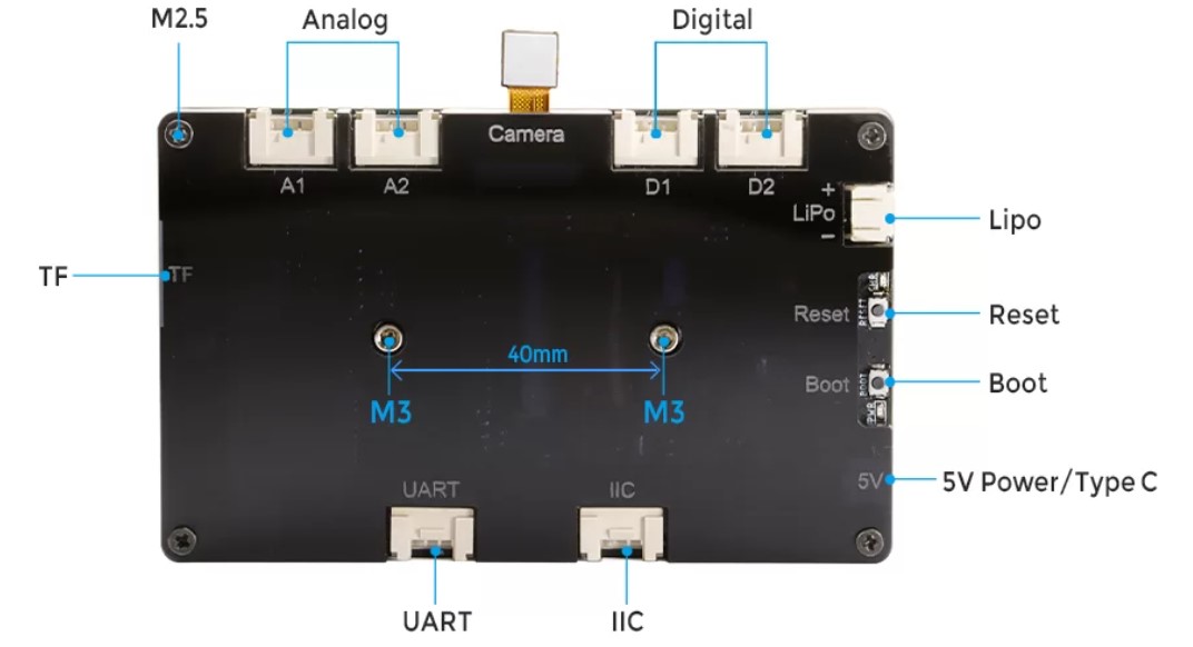
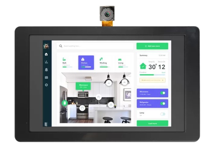
With a strong ESP32-S3 chip, 2.4GHz Wi-Fi compatibility, and Bluetooth 5 (LE), this handheld terminal is built on the powerful ESP32 controller which offers enhanced computing and processing capabilities for IoT terminal applications. The ESP32-S3-N16RB module can lead to a variety of interfaces due to its scalability. It incorporates a MEMS microphone, camera interface, and buzzer function in addition to Crowtail’s digital port, analog port, UART, and IIC interface.
It has made it simple to recognize faces, objects, and scenes with the 2M pixel camera, and it allows for greater creativity in advanced applications like speech recognition and voice control. The 3.5-inch screen, which uses an SPI serial display with 320 x 480 resolution, is the finest option for a handheld or pocket terminal. The screen’s frame rate can reach 20FPS, which is adequate for the majority of application settings.
Video
Software
It is compatible with Python, MicroPython, and Arduino and facilitates the creation of ESP-IDF and Arduino IDE. Additionally, it supports LVGL, the most widely used free and open-source embedded graphics library for building stunning user interfaces for any MCU, MPU, and display type.
Specifications
Core Processor – ESP32-S3
Memory – 16MB Flash 8MB PSRAM
Maximum Speed – 240Mhz
Wi-Fi – 802.11 a/b/g/n 1×1,2.4 GHz band supports 20 and 40 MHz bandwidth, Supports Station, SoftAP, and SoftAP + Station mixed modes.
Bluetooth – BLE 5.0
LCD Screen
-Resolution – 320 x 480
-Display Size – 3.5 inch
-Touch – Capacitive Touch
-Interface – SPI Interface
Camera- OV2640, 2M Pixel
Microphone- MEMS Microphone
SD Card – Onboard SD Card Slot1x I2C
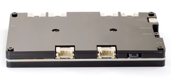
I/O Interface 1x USB C, 1x UART, 2x Analog, 2x Digital
Others:
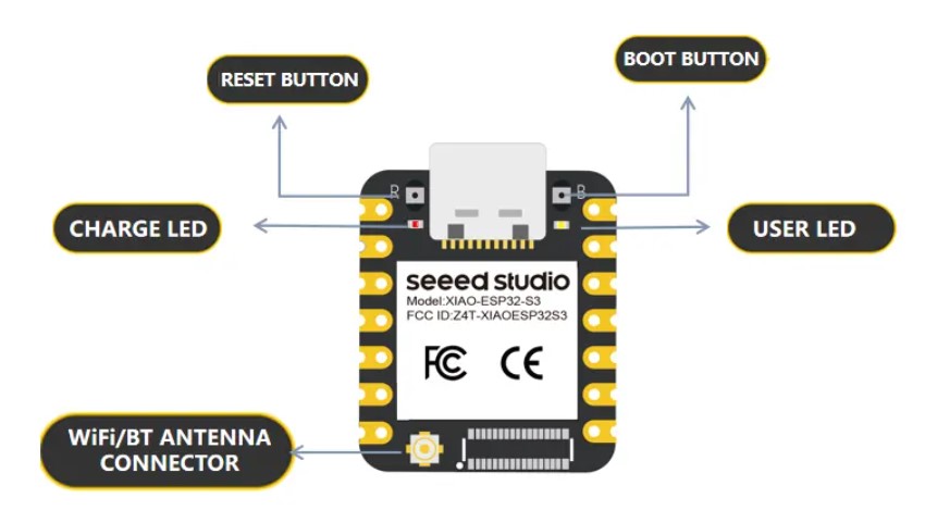
– REST Button
-BOOT Button
Power- USB DC 5 V, lithium battery 3.7 V
-Average current 83 mA
Operating Temperature : -10°C ~ 65°C
Dimension Size – 106 x 66mm x 13mm
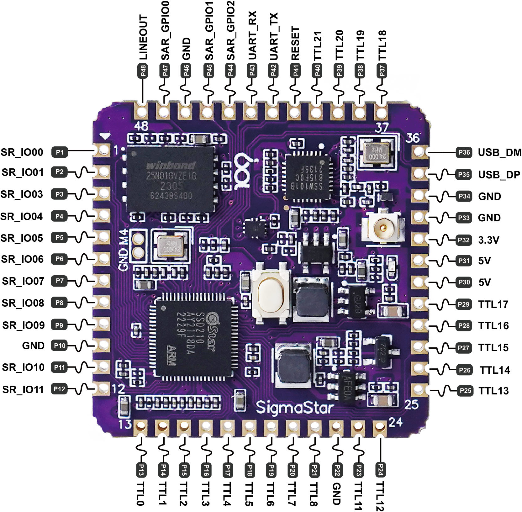
Pinout
The entire terminal is encircled by a flawless acrylic shell, which enhances the beauty of the entire product. It can be mounted to the wall or a PLC rail. The wiki page gives detailed information.
Applications
It can be paired with 150+ different types of Crowtail modules to finish more engaging projects. It is appropriate for a variety of situations, including industrial IoT control terminals, smart agriculture terminals, individualized smart home monitoring terminals, and individualized DIY projects. It can do face recognition and video surveillance as the central control screen of a smart home, enabling users to monitor household activities.
Purchase Information
ESP32 S3 Terminal can be brought for $39.90 from the Elecrow website.
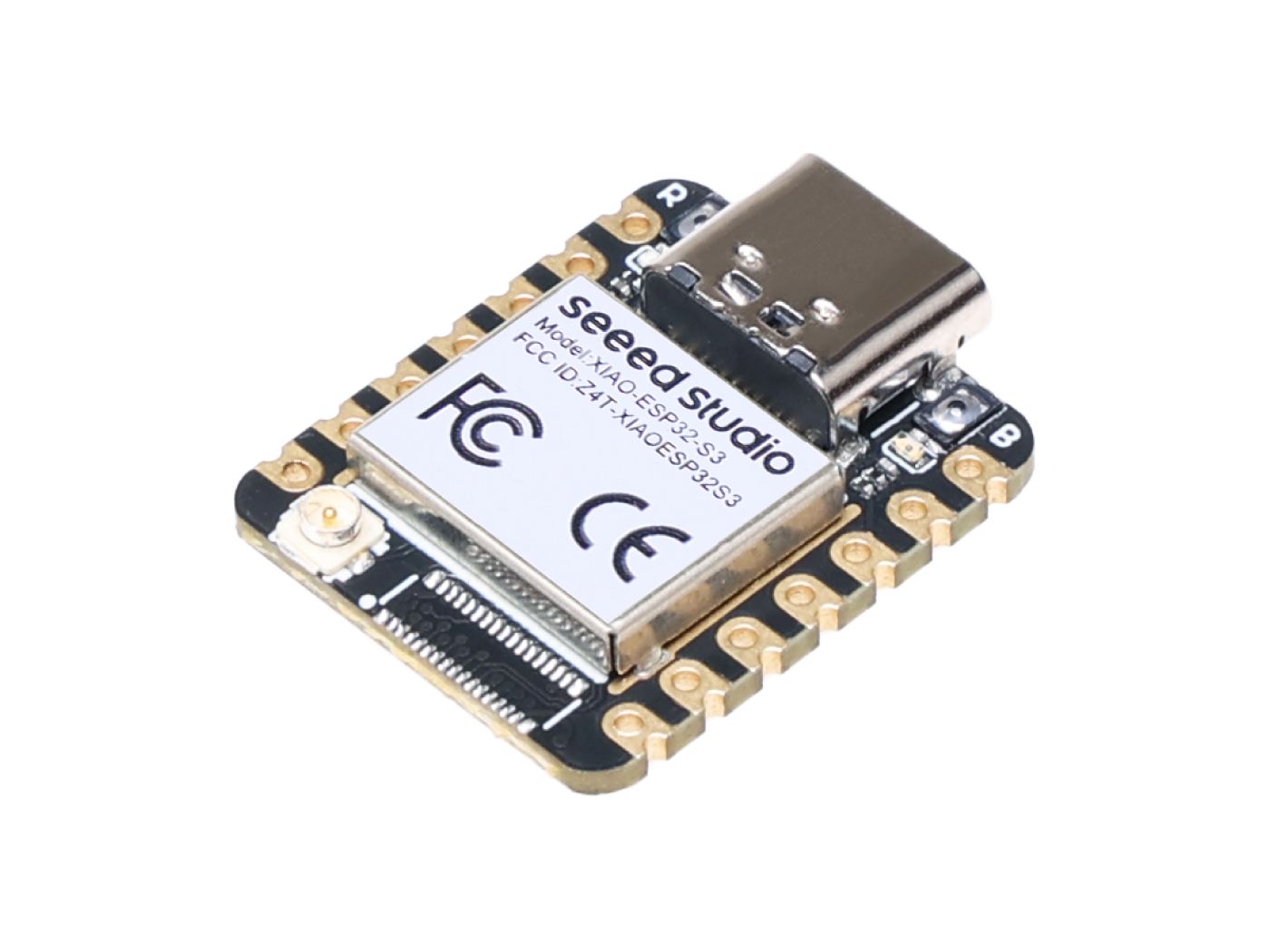
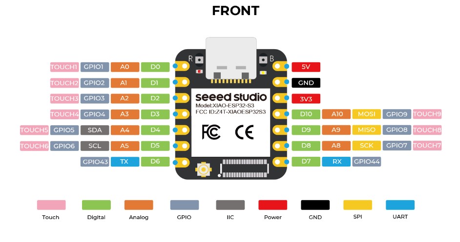
The Seeed Studio XIAO Series are tiny development boards with a thumb-sized size and a comparable hardware architecture. The Seeed Studio XIAO ESP32S3 uses a 240MHz Xtensa 32-bit LX7 dual-core processor, allowing WiFi and Bluetooth 5.0 wireless connectivities, deep sleep mode with power consumption as low as 14 μA, and lithium battery charging management. It serves as the ideal option for robotics, smart homes, wireless wearable technology, and the Internet of Things. The 32-bit RISC-V-based XIAO ESP32C3 was introduced last year.
The XIAO ESP32S3 is designed to easily handle a variety of challenging multitasking assignments thanks to its powerful Xtensa 32-bit LX7 dual-core processor, 8MB PSRAM, and 8MB Flash memory.
Features
Powerful MCU Board: Include the ESP32S3 32-bit, dual-core, Xtensa CPU, mounted multiple development ports, and it also supported by Arduino/MicroPython
Outstanding RF performance: Supports 2.4GHz WiFi and BLE 5.0 dual wireless communication, and when linked to a U.FL antenna, supports remote communication of up to 100 meters.
Extensive Power Design: Lithium batteries have the ability to manage their charge, and four power consumption models are available. These models enable deep sleep mode, which has a power consumption as low as 14 μA.
Thumb-sized Compact Design: 21 x 17.5mm, adopting the traditional XIAO form factor, appropriate for applications with limited space, such as wearable devices.
Seeed Studio XIAO ESP32S3 Specifications:
Processor- ESP32-S3R8
-Xtensa LX7 dual-core, 32-bit processor running up to 240 MHz
Wireless connectivity-Complete 2.4GHz WiFi subsystem, Bluetooth 5.0, Bluetooth mesh
On-chip Memory- 8M PSRAM & 8MB Flash
Interface- 1x UART, 1x IIC, 1x IIS, 1x SPI,11x GPIO(PWM), 9x ADC, 1x User LED
Others
-1x Charge LED
-1x Reset button, 1x Boot button
Power- Input voltage (Type-C): 5V
-Input voltage (BAT): 4.2V
-Charging battery current: 50mA
Low Power Consumption Model
(Supply Power: 3.8V)
-Modem-sleep Model: ~ 25 mA
-Light-sleep Model: ~ 2mA
-Deep Sleep Model: ~ 14 μA
WiFi-Enabled Power Consumption
-Active Model: ~ 100 mA
BLE Enabled Power Consumption
-Active Model: ~ 85 mA
Dimensions- 21 x 17.5mm
Working Temperature -40°C ~ 65°C
Pinout
Application:
The Internet of Things, wearable devices, smart homes, robotics, health monitoring, education, Rapid prototyping, and low-power (LP) networking are just some of the fields that could benefit from its use.
Purchase Information
XIAO ESP32S3 is available for $7.49 on the product page. In addition, SeeedStudio stated that they will soon be releasing a comparable XIAO ESP32S3 model with a built-in camera and microphone.
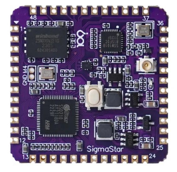
The DongshanPI-PicoW is a tiny Arm Linux board that features four 12-pin headers in addition to the SSW101B USB WiFi chip. According to its name, the DongshanPI-PicoW board or module is intended to be an Arm Linux alternative to the Raspberry Pi Pico W. It features a SigmaStar SSD210 dual-core Cortex-A7 processor with 64MB RAM, an SSW101B USB WiFi 4 chip, and a considerable quantity of input and output connections.
The DongshanPI-PicoW development board is made up of Sigma Technology and has SSD210 and SSW101B WiFi. The design utilizes a 2.0mm pin header in conjunction with a stamp hole. To start up and make use of the development board system, it merely requires input from a 5V power supply.
The module also includes a 128 MB SPI flash to run Linux and provides a display interface up to 1280 x 800 60fps, USB 2.0, audio interfaces, and more interfaces in a small 31 mm x 31 mm form factor with 48 through and castellated holes that are easy to incorporate into compact devices.
Specifications
Processor – SigmaStar SSD210 ARM Cortex-A7 Dual Core 1 GHz with Neon and FPU
Four 12-pin 2.0mm pitch headers with castellated holes
Max. two MIPI interfaces with 2 or 1 data lane and 2 clock lanes
TTL output up to 1280×800 60fps
MIC and DMIC inputs, lineout I2S TDM 8-channel, RX 2/4/8 channels, TX 2 channels
SDIO 2.0 x1
SPI x2 I2C x2 UART x4 PWM x4
USB 2.0 x1
64MB DDR2
SSW101B
32Bit RISC 150MHz CPU
Support HT20/40MHz Bandwidth
Networking – Ethernet x1
Security Engines
Others – Reset button
Power – 5V via I/O pins
Dimensions – 31 x 31 mm (estimated)
Pinout
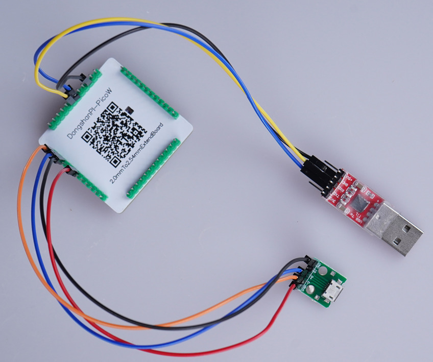
As shown in the picture below, the user must join the pins of the core board to the pins of the adapter board. Users can connect this bottom board to the hole board.
The Wiki contains some important information, as well as schematics, a Linux image, and flashing tools. Any concerns regarding this circuit board’s development can be discussed on their forum.
Purchase Information
On Aliexpress, the DongshanPI-PicoW can be purchased for $6.71 USD.
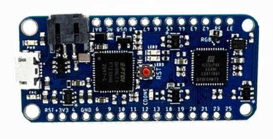
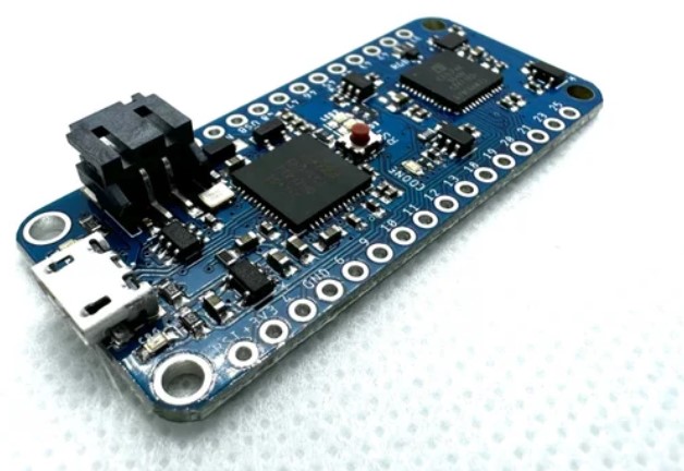
With the help of this exclusive IcyBlue FPGA feather developed by OAK DEV TECH, it is simple to launch an FPGA development project using powerful and dependable ICE5LP4K FPGA from Lattice Semiconductor. The ICE5LP4K includes two hardware I2C and SPI blocks, a bright RGB LED, two user LEDS, and 22 user-accessible GPIO that can be accessed through the headers on the feather board.
A Low Power FPGA Development Board
The IcyBlue Feather is an FPGA development board that features a user-friendly interface and a conventional form factor. This FPGA has low power and was developed specifically for mobile and other applications that are power conscious. IcyBlue offers a user interface that is simple to program through the use of an FTDI FT232H USB to FIFO bridge. This interface may be used to either program the FPGA directly in the IcyBlue base model or an SPI FLASH chip on the board that is meant for permanent project deployment.
As mentioned, users may easily program the onboard SPI FLASH with bitstream hex or bin files by utilizing an FTDI FT232HQ USB FIFO bridge, which makes programming simple and easy to accomplish. This board may now be used with both open source tools such as icestorm and proprietary tools such as the Diamond Programmer, which is offered by Lattice Semiconductor. This compatibility is made possible by the FT232HQ.
Specifications
3520 LUTs / 440 LABs
2MB SPI FLASH
Built-in USB FIFO Bridge via FT232H
I/O Interface: 22 X GPIO
Others: 1 x Bright RGB LED
-2 x User LEDs
Power: LiPo Battery Charging for 1S LiPo Batteries
2x Hardened SPI IP Cores
2x Hardened I2C IP Cores
This project is mobile and powered by a battery thanks to Adafruit’s feather form factor, which was developed for the project. This is especially helpful for building FPGA projects while on the go and for mobile deployments of those projects.
The IcyBlue Feather delivers a strong and capable yet compact FPGA to the workstation, regardless of developing an FPGA for the first time or being a seasoned professional in the field.
Purchase Information
IcyBlue Feather – The ICE5LP4K Feather Development Board can be preordered for $69.95 from the OAK DEV TECH. On the product website, it is stated that the price of preorders has been lowered for a limited time in order to make the board available to a greater number of individuals. In addition to this, it adds that the product photo that is now being displayed is a prototype and that the final product will be blue with a white solder mask.
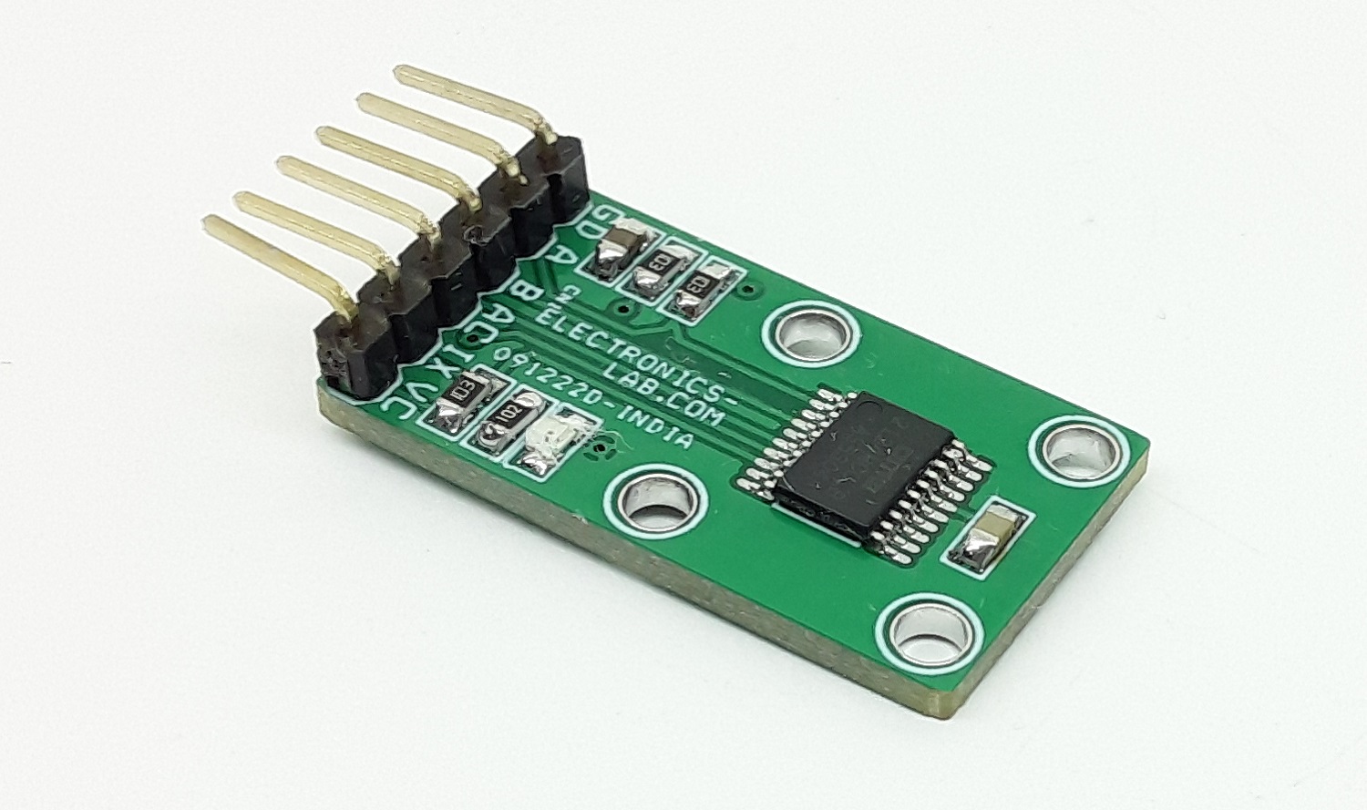
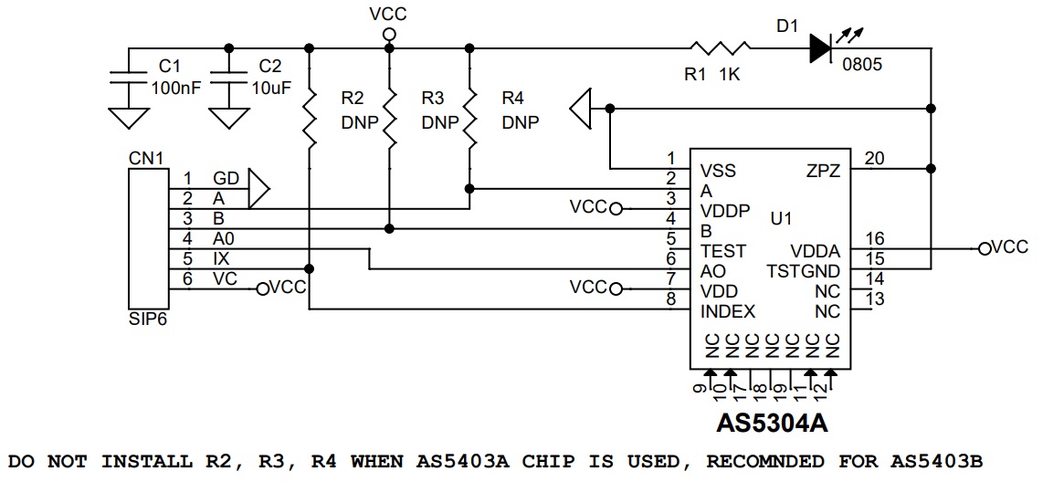
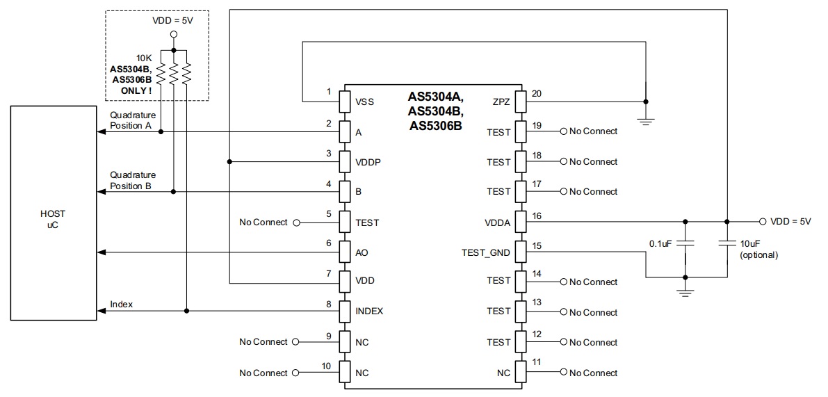
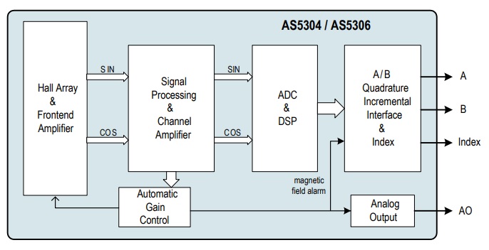
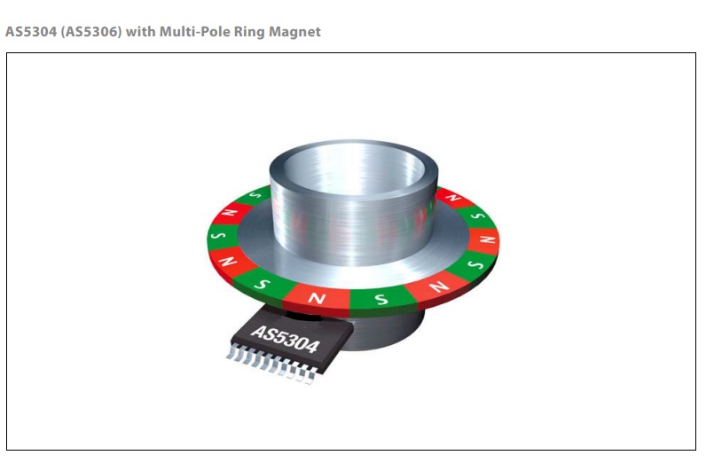
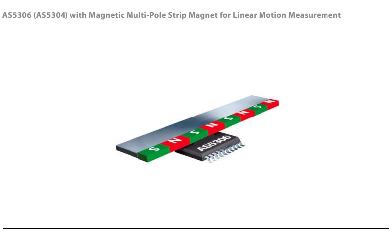
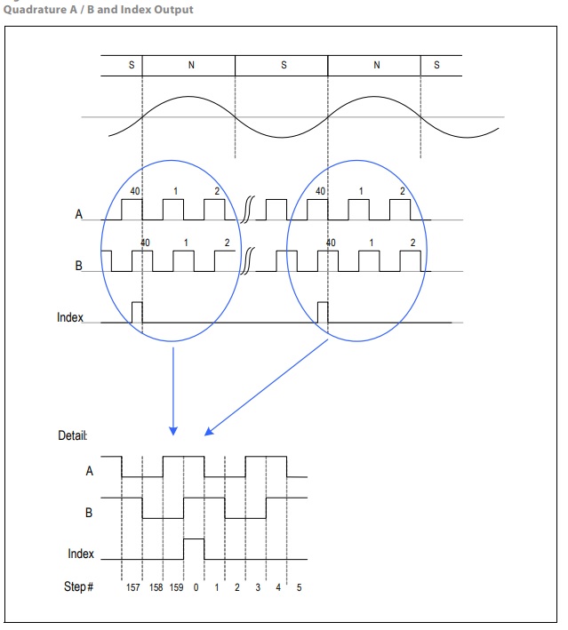
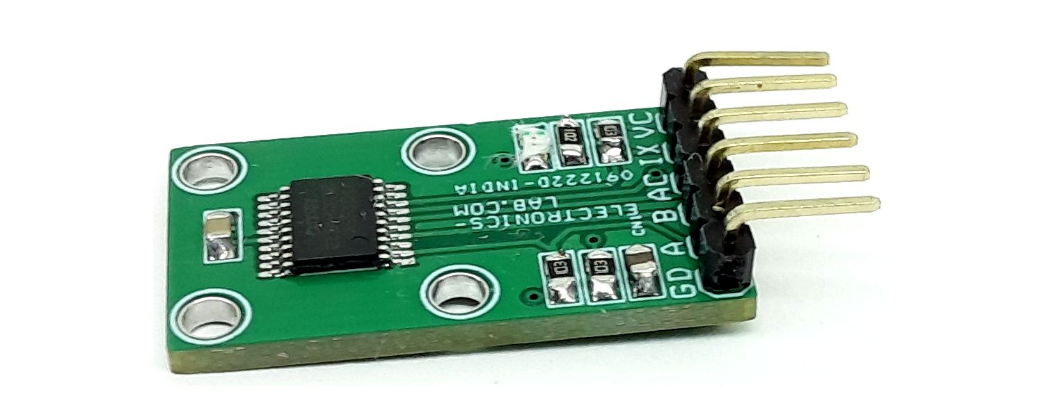
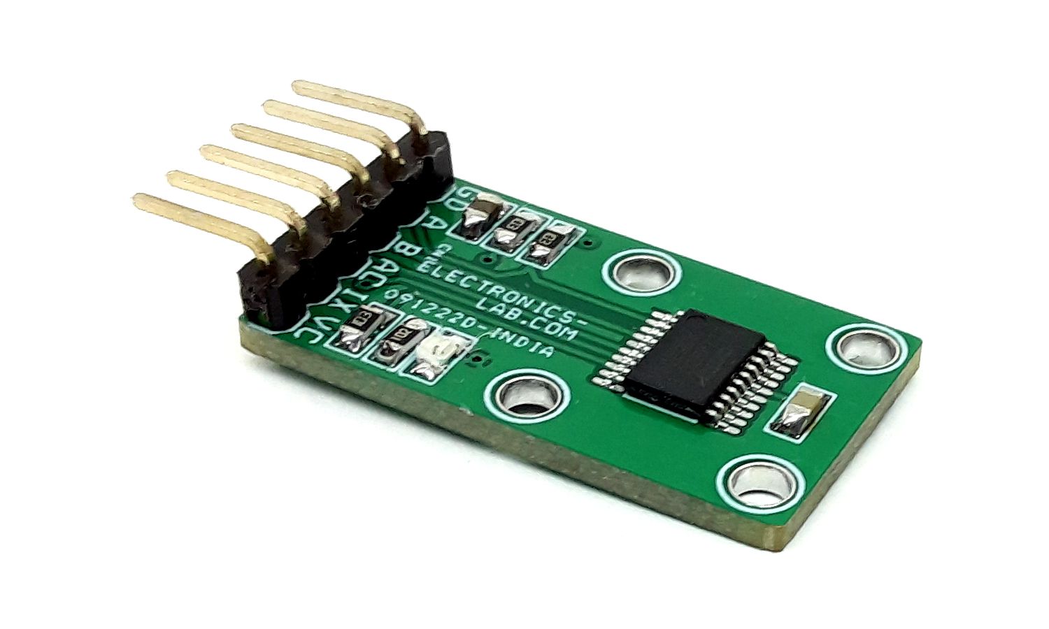
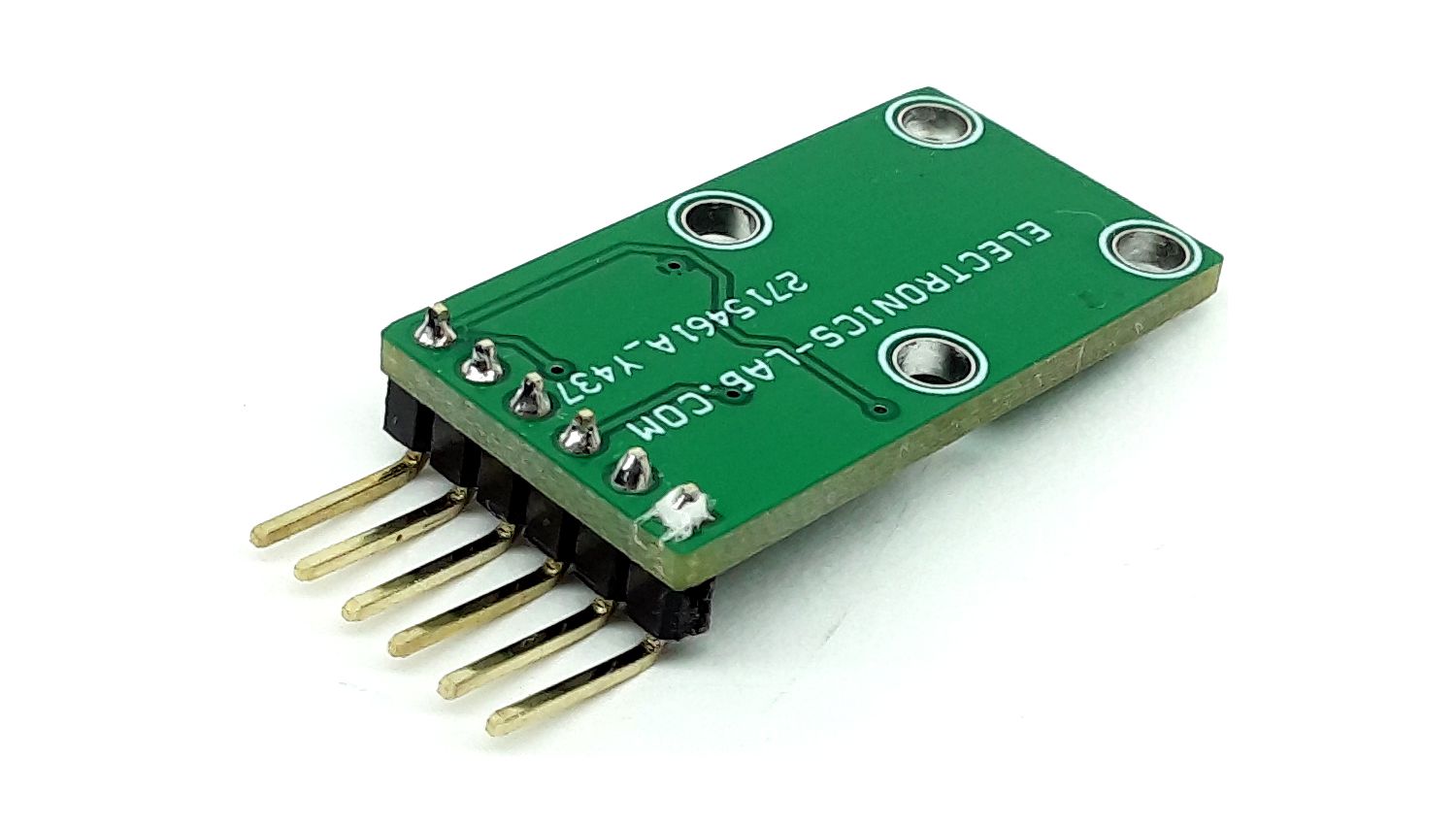
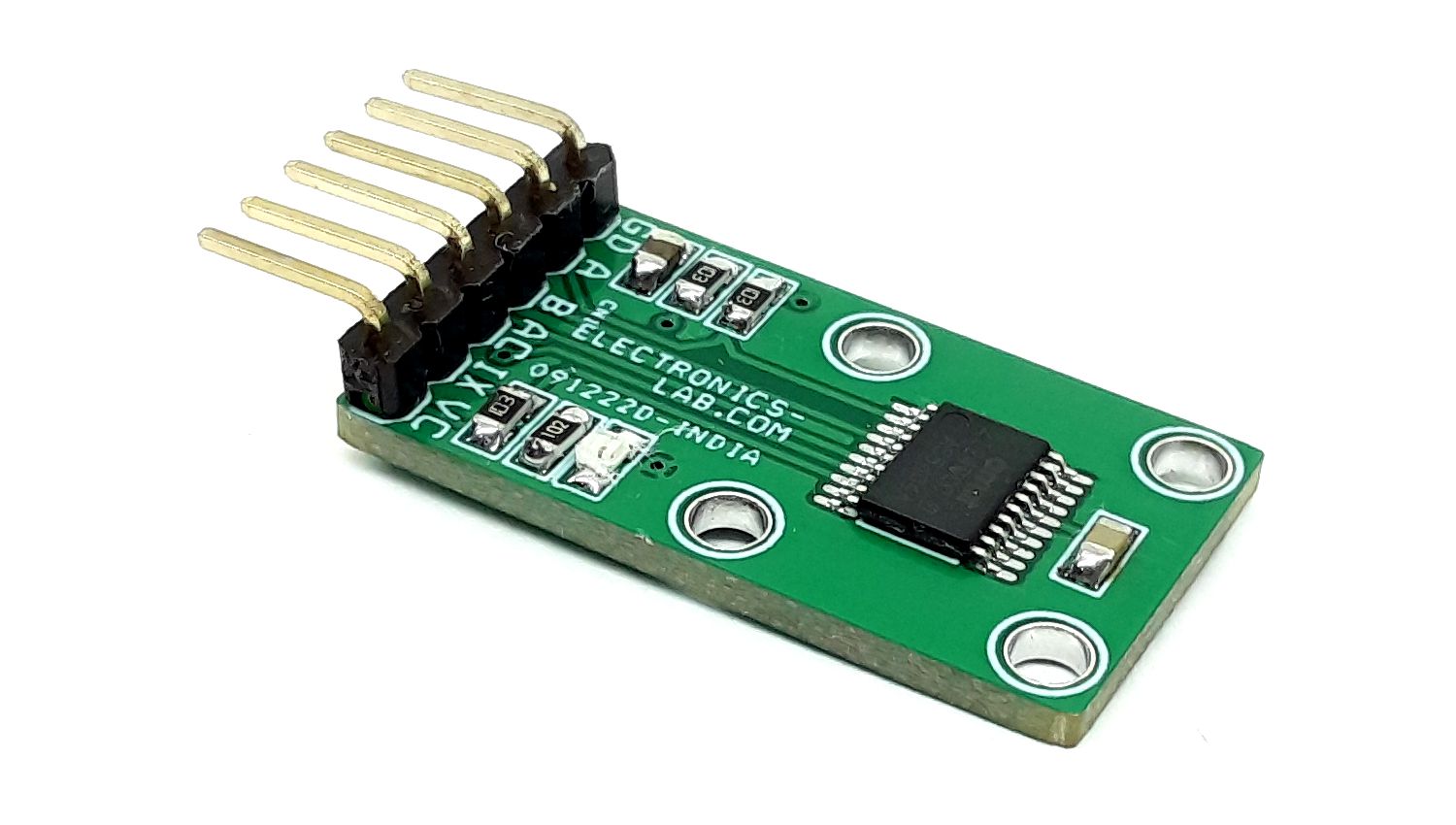
This sensor module is a simple solution to build a magnet-based rotary encoder. The project is based on the AS5304 chip with integrated Hall elements for measuring linear or rotary motion using multi-pole magnetic strips or rings. This allows the usage of the module in applications where the Sensor IC cannot be mounted at the end of a rotating device (e.g. at hollow shafts). Instead, the module is mounted off-axis underneath a multi-pole magnetized ring or strip and provides a quadrature incremental output with 40 pulses per pole period at speeds of up to 20 meters/second. A single index pulse is generated once for every pole pair at the Index output. Using, for example, a 32-pole-pair magnetic ring, the module can provide a resolution of 1280 pulses/revolution, which is equivalent to 5120 positions/revolution or 12.3bit. The maximum speed at this configuration is 9375 rpm. Recommended pole pair length is 4mm (2mm north pole / 2mm south pole). The chip accepts a magnetic field strength down to 5mT (peak).
Features
5V to 5.5V operating voltage
Current Consumption 30 to 40mA
High speed, up to 20m/s
Magnetic pole pair length: 4mm
Resolution of 1280 Pulses/Revolution
Resolution: 25μm
40 pulses / 160 positions per magnetic period
Quadrature Output Index, Channel A and Channel B with Pullups
AO – AGC Analog Output. (Used to detect low magnetic field strength)
1 index pulse per pole pair
Linear movement measurement using multi-pole magnetic strips
Circular off-axis movement measurement using multi-pole magnetic rings
Magnetic field strength indicator, magnetic field alarm for end-of-strip or missing magnet
PCB Dimensions 29.21 x 15.88mm
4 x 2.5mm Mounting Holes
Benefits and Key Features
Contactless motion and position sensing
High-speed measurement
Robust against external magnetic stray fields
Highest reliability and durability in harsh environments
Control of high-speed movements
Lower material cost (no magnetic shielding needed)
Magnet
Magnetic pole length 2mm
Magnetic pole pair length 4mm
Magnetic amplitude 10-60mT
Magnetic offset +/-0.5mT
Connections and Other Details
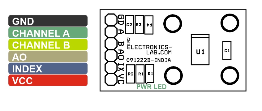
CN1: Pin 1 = GND, Pin 2 = Channel A Out, Pin 3 = Channel B Out, Pin 4 = AO Out, Pin 5 = Index Out, Pin 6 = VCC
D1: Power LED
Outputs
Incremental quadrature position output A. Short circuit current limitation
Incremental quadrature position output B. Short Circuit Current Limitation
Index output, active HIGH. Short Circuit Current Limitation
AGC Analog Output. (Used to detect low magnetic field strength)
Incremental Quadrature AB Output
The digital output is compatible with optical incremental encoder outputs. The direction of rotation is encoded into two signals A and B that are phase-shifted by 90º. Depending on the direction of rotation, A leads B (CW) or B leads A (CCW).
Index Pulse
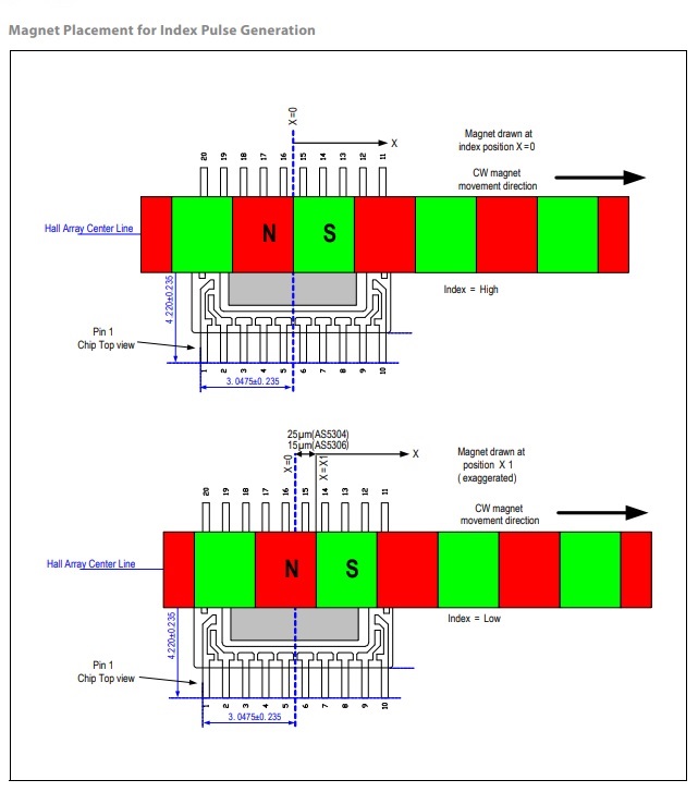
A single index pulse is generated once for every pole pair. One pole pair is interpolated to 40 quadrature pulses (160 steps), so one index pulse is generated after every 40 quadrature pulses. The Index output is switched to Index = high, when a magnet is placed over the Hall array, the north pole of the magnet is placed over the left side of the IC (top view, pin#1 at bottom left) and the south pole is placed over the right side of the IC. The index output will switch back to Index = low, when the magnet is moved by one LSB from position X=0 to X=X1. One LSB is 25μm.
The AO Output
The Analog Output (AO) provides an analog output voltage representing the Automatic Gain Control (AGC) of the Hall sensors signal control loop. This voltage can be used to monitor the magnetic field strength and hence the gap between the magnet and chip surface:
Short distance between magnet and IC -> strong magnetic field -> low loop gain -> low AO voltage
Long distance between magnet and IC -> weak magnetic field -> high loop gain -> high AO voltage
Magnetic Field Warning Indicator
The Module can also provide a low magnetic field warning to indicate a missing magnet or when the end of the magnetic strip has been reached. This condition is indicated by using a combination of A, B and Index, which does not occur in normal operation: A low magnetic field is indicated with: Index = high A=B=low
Vertical Distance between Magnet and IC
The recommended vertical distance between the magnet and IC depends on the strength of the magnet and the length of the magnetic pole. Typically, the vertical distance between magnet and chip surface should not exceed ½ of the pole length. That means for the AS5304 module, having a pole length of 2.0mm, the maximum vertical gap should be 1.0mm. These figures refer to the chip surface. Given a typical distance of 0.2mm between chip surface and IC package surface, the recommended vertical distances between the magnet and IC surface are therefore: AS 5304: ≤ 0.8mm
Soft Stop Feature for Linear Movement Measurement
When using long multi-pole strips, it may often be necessary to start from a defined home (or zero) position and obtain absolute position information by counting the steps from the defined home position. The AS5304 module provides a soft stop feature that eliminates the need for a separate electro-mechanical home position switch or an optical light barrier switch to indicate the home position. The magnetic field warning indicator (see Magnetic Field Warning Indicator- refer datasheet of chip) together with the index pulse can be used to indicate a unique home position on a magnetic strip:
Firstly, the AS5304 module moves to the end of the strip until a magnetic field warning is displayed (Index = high, A=B=low).
Then, the AS5304 module moves back towards the strip until the first index position is reached (Note that an index position is generated once for every pole pair, it is indicated with: Index = high, A=B= high). Depending on the polarity of the strip magnet, the first index position may be generated when the end of the magnet strip only covers one-half of the Hall array. This position is not recommended as a defined home position, as the accuracy of the AS5304 module are reduced as long as the multi-pole strip does not fully cover the Hall array. 3. It is therefore recommended to continue to the next (second) index position from the end of the strip (Index = high, A=B= high). This position can now be used as a defined home position.
Incremental Hysteresis
If the magnet is sitting right at the transition point between two steps, the noise in the system may cause the incremental outputs to jitter back and forth between these two steps, especially when the magnetic field is weak. To avoid this unwanted jitter, a hysteresis has been implemented.
Resolution and Maximum Rotating Speed
When using the AS5304A module in an off-axis rotary application, a multi-pole ring magnet must be used. Resolution, diameter and maximum speed depend on the number of pole pairs on the ring.
Resolution
The angular resolution increases linearly with the number of pole pairs. One pole pair has a resolution (= interpolation factor) of 160 steps or 40 quadrature pulses.
Resolution [steps] = [interpolation factor] x [number of pole pairs] Resolution [bit] = log (resolution[steps]) / log (2) Example: Multi-pole ring with 22 pole pairs Resolution = 160×22 = 3520 steps per revolution = 40×22 = 880 quadrature pulses / revolution = 11.78 bits per revolution = 0.1023° per step
Multi-Pole Ring Diameter
The length of a pole pair across the median of the multi-pole ring must remain fixed at either 4mm. Hence, with increasing pole pair count, the diameter increases linearly with the number of pole pairs on the magnetic ring.
Magnetic ring diameter = [pole length] * [number of pole pairs] / π for AS5304 module: d = 4.0mm * number of pole pairs / π
Example: (same as above) multi-pole ring with 22 pole pairs for AS5304 Ring diameter = 4 * 22 / 3.14 = 28.01mm (this number represents the median diameter of the ring.
Maximum Rotation Speed
The AS5304 module uses a fast interpolation technique allowing an input frequency of 5kHz. This means it can process magnetic field changes in the order of 5000 pole pairs per second or 300000 revolutions per minute. However, since a magnetic ring consists of more than one pole pair, the above value must be divided by the number of pole pairs to get the maximum rotation speed: Maximum rotation speed = 300000 rpm / [number of pole pairs] Example: (same as above) multi-pole ring with 22 pole pairs: Maximum speed = 300000 / 22 = 13636 rpm (this is independent of the pole length)
Maximum Linear Travelling Speed
For linear motion sensing, a multi-pole strip using equally spaced north and south poles is used. The pole length is again fixed at 2.0mm for the module As shown in Maximum Rotation Speed above, the sensors can process up to 5000 pole pairs per second, so the maximum traveling speed is: Maximum linear travelling speed = 5000 * [pole pair length] Example: Linear multi-pole strip: Maximum linear travelling speed = 4mm * 5000 1/s = 20000mm/s = 20m/s {for AS5304 module}
Note1: The project also can accommodate pin to pin compatible chip AS5606B
Note2: AS5403A chip has internal pullups and thus doesn’t require Pull up resistors R2, R3, and R4. For AS5403B chip is an open drain type and requires 10K pullup resistors R2, R3, R4
Applications
The module is ideal for high-speed linear motion and off-axis rotation measurements in applications, such as electrical motors, X-Y-stages, rotation knobs, and industrial drives.
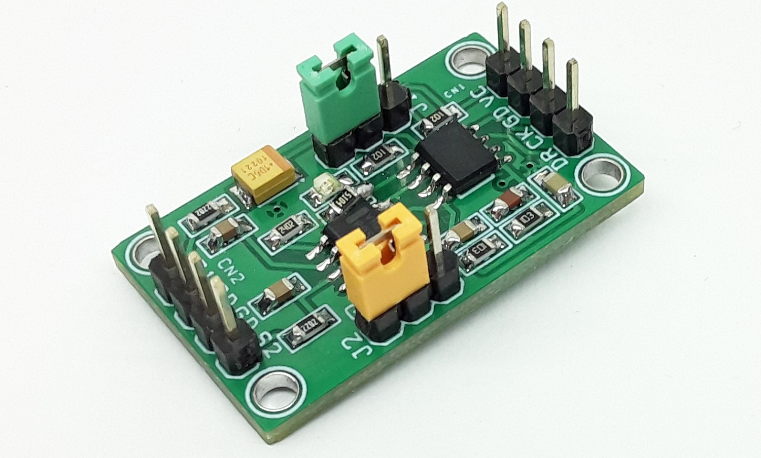
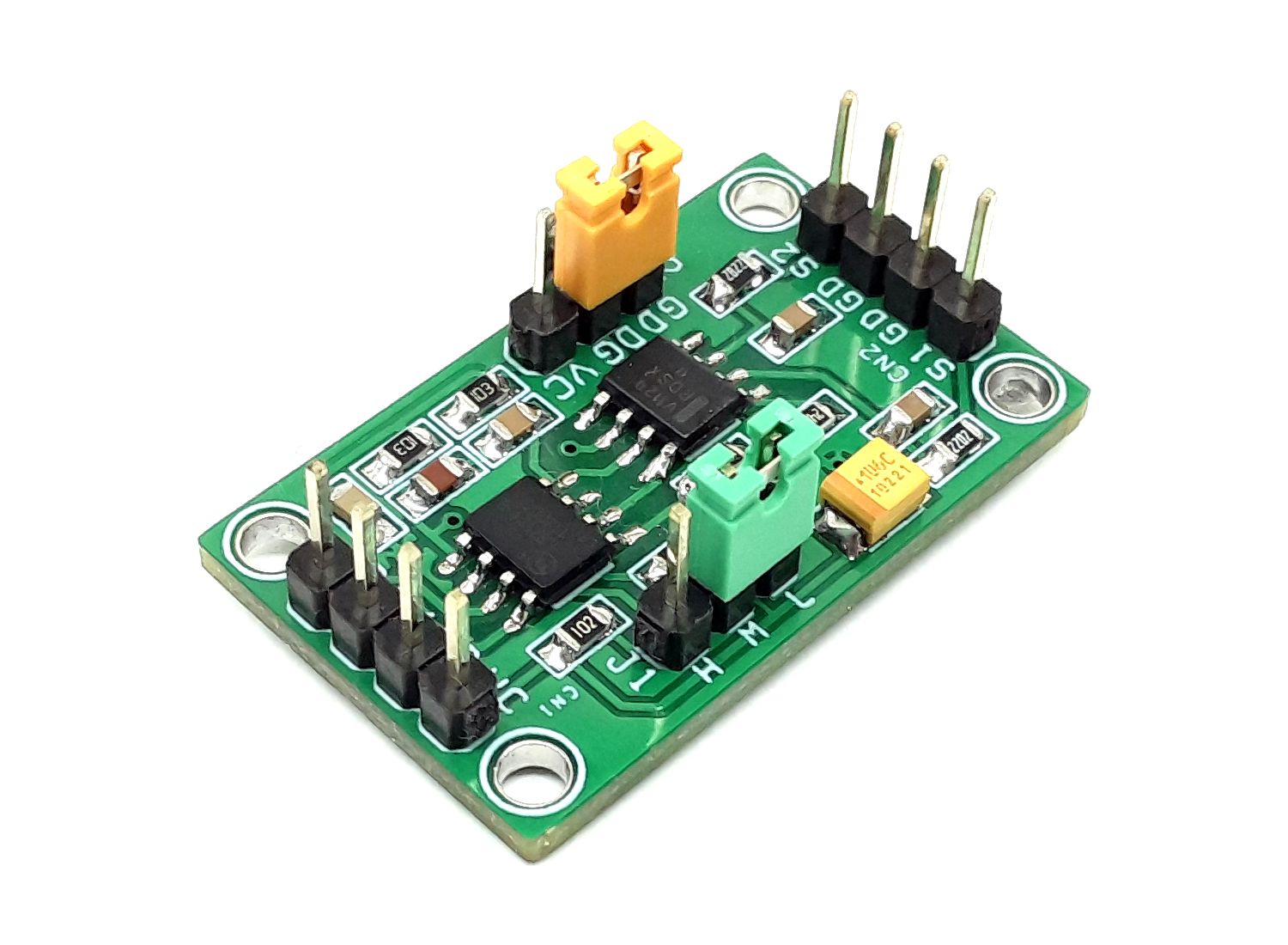
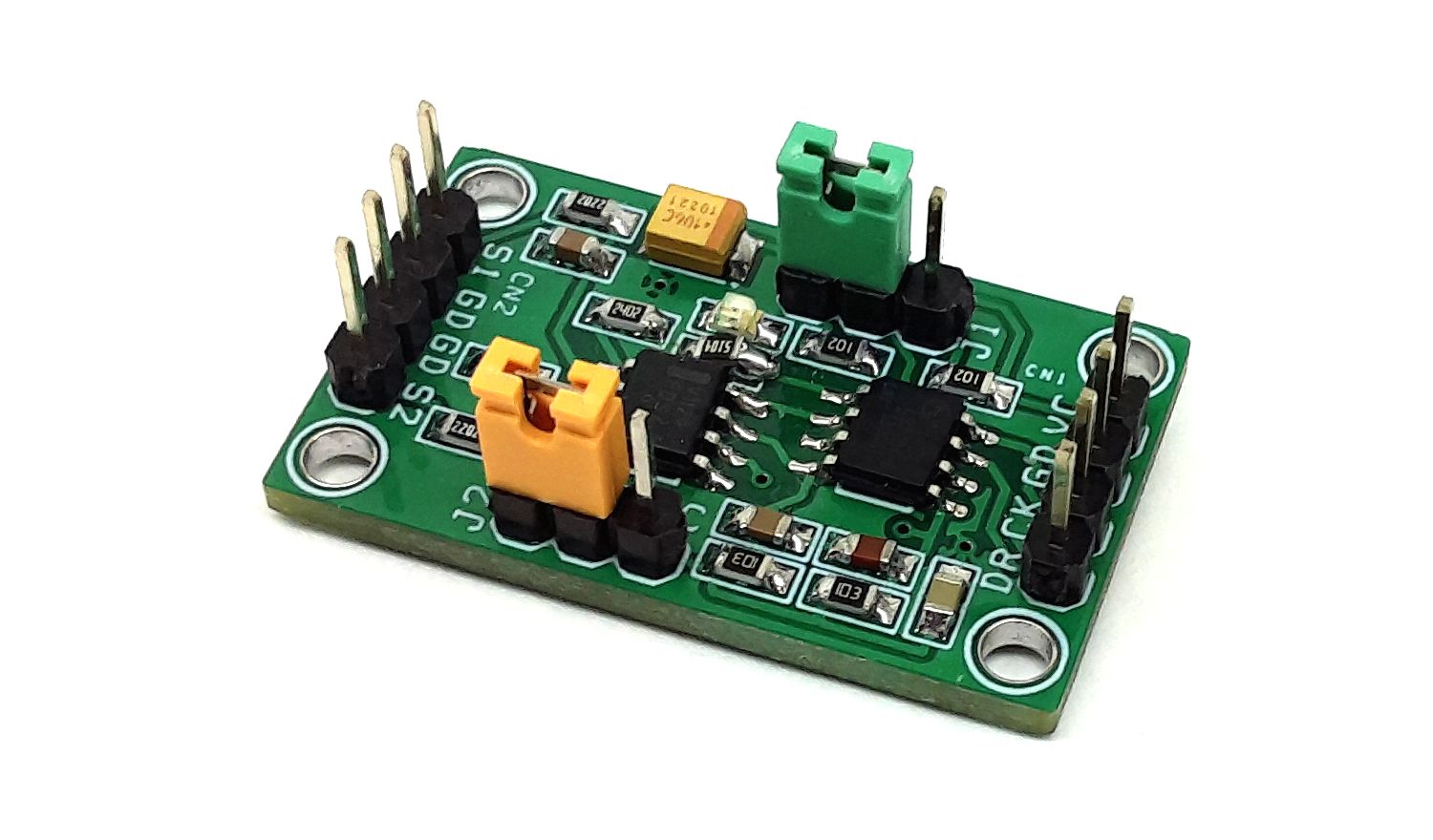
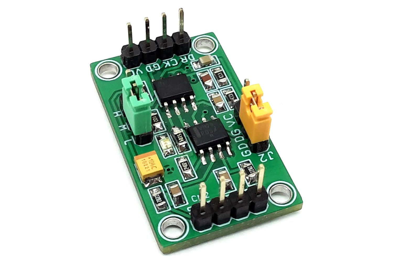
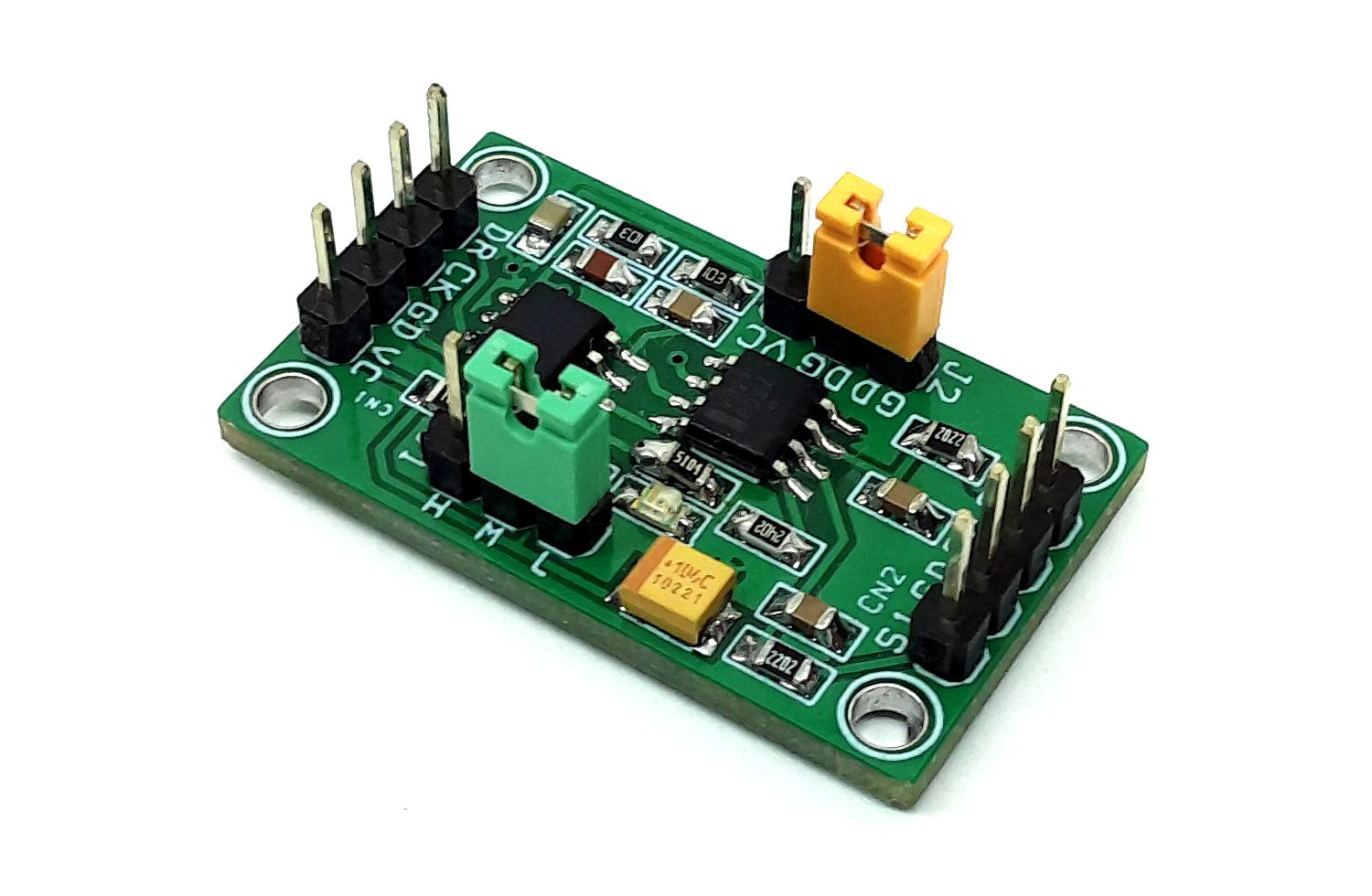
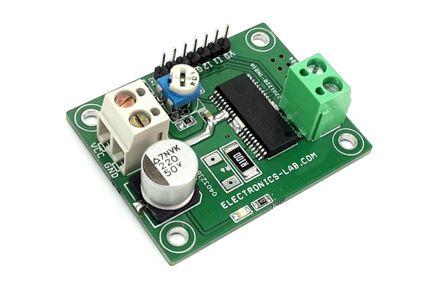
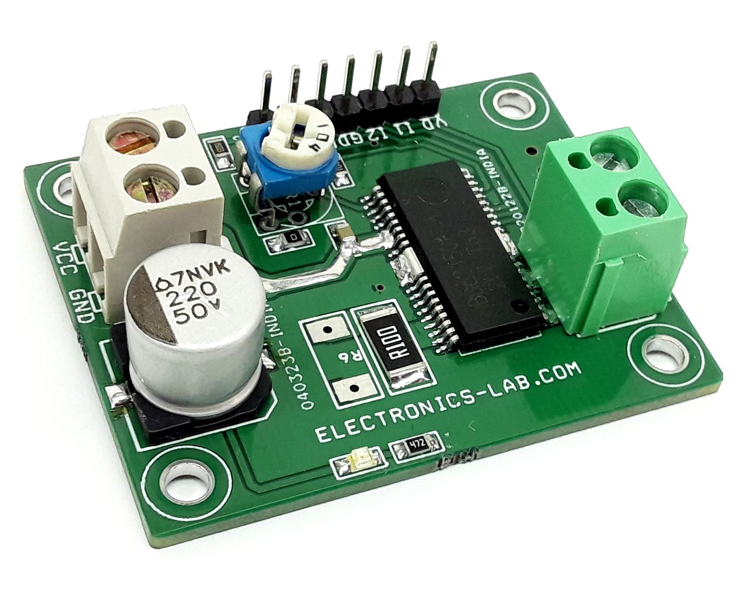
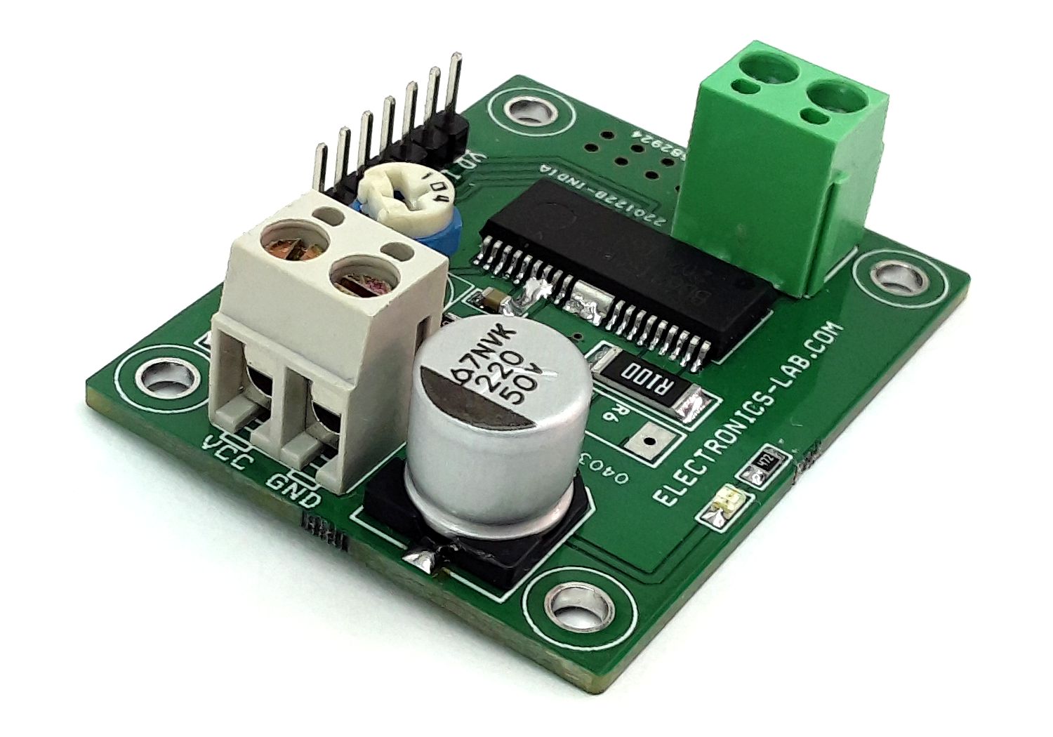
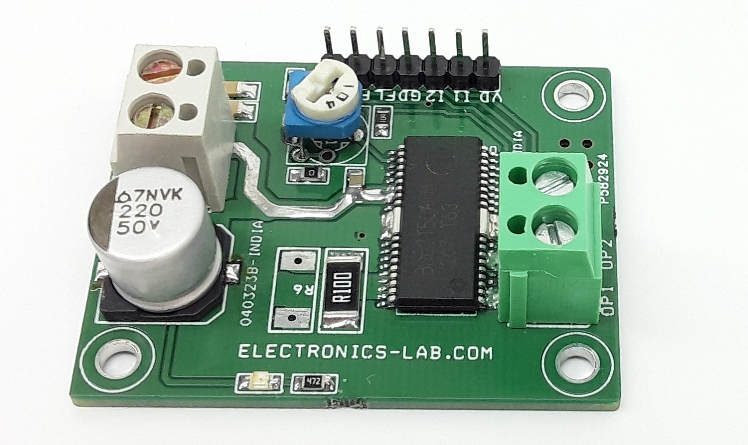
This project enables the users to use a stepper motor as a rotary encoder for position control and Up/Down direction control. A bipolar stepper motor can be used as a rotary sensor as it generates two channel strings of pulses by turning the shaft. The circuit provides Step pulse and Up/Down Direction signals by rotating the stepper motor shaft clockwise or counterclockwise directions. The outputs are TTL logic signals. The operating supply is 5V DC and the circuit consumes very low current.
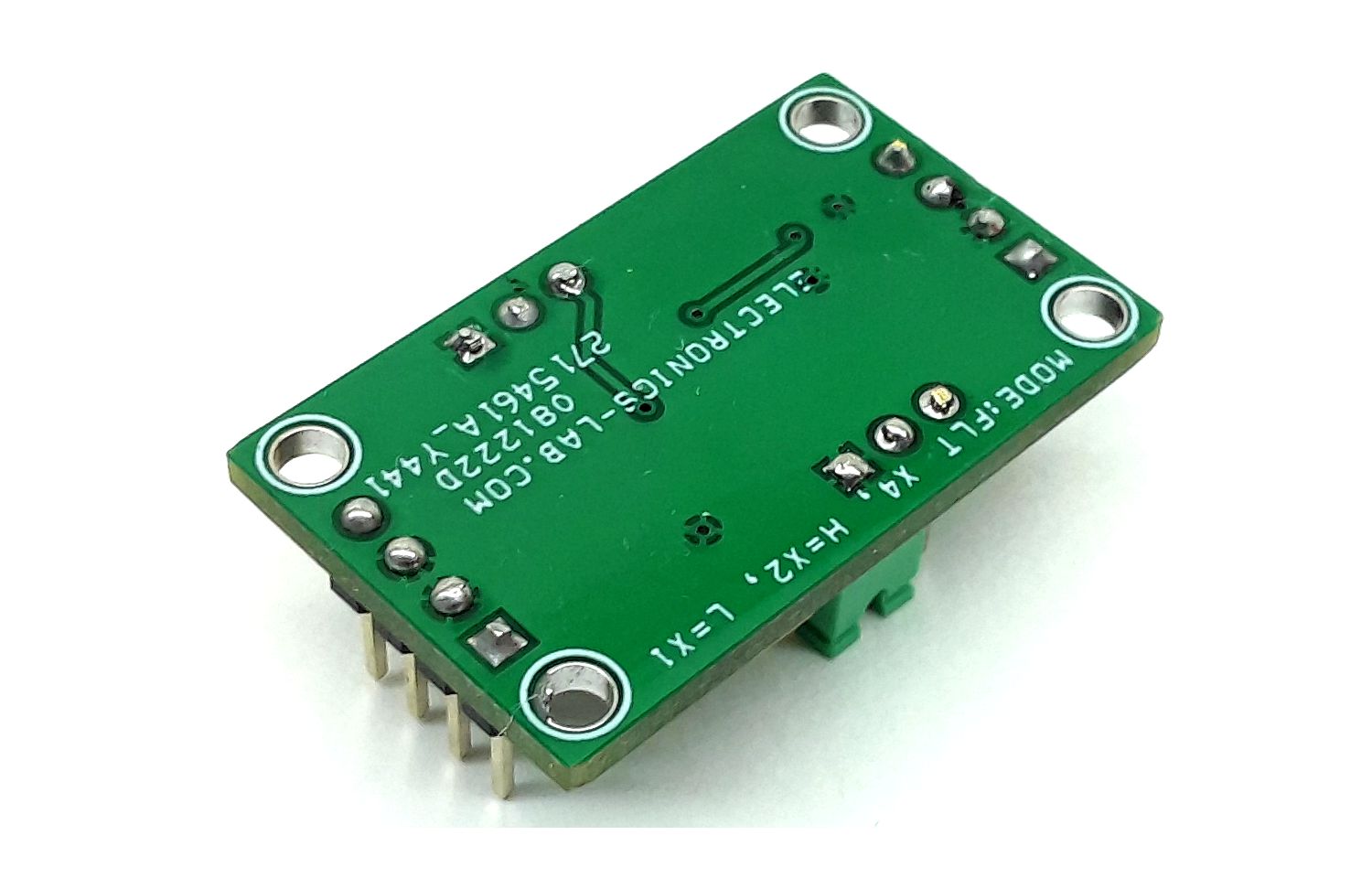
Mode Selection Jumper J1
Mode has a 3-states to select output resolutions X1, X2, and X4. The input quadrature clock rate is multiplied by factors of 1,2 and 4 in X1, X2, and X4 mode respectively, in the producing output.
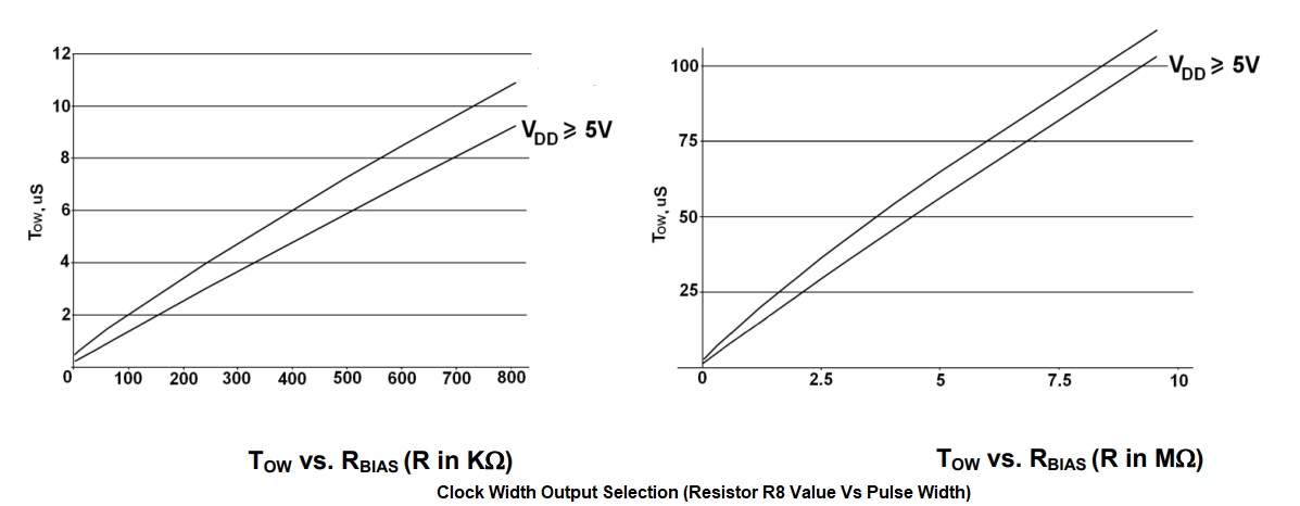
RBIAS– Resistor R8 (Range 2K Ohm to 10M Ohms) – Refer to Figure below
The value of this resistor is responsible for the output clock pulse width. Alter the value to change the output pulse width. Refer to the datasheet for more info.
When the shaft of the stepper motor is turned two coils of the bipolar stepper motor generate two electrical signals which are connected to IN1 and IN2 of the U1 NCV1124 chip. The chip continuously compares the stepper motor output signal to a user−programmable internal reference. An alternating input signal of appropriate amplitude at IN1 or IN2 results in a rectangular waveform at the corresponding OUT terminal OP1 and OP2, both these signals are interfaced to the LS7184 quadrature clock converter. When both signals are applied to the A and B inputs of the LS7184 they are converted to Clock and Up/Down direction control. These outputs can be interfaced directly with standard Up/Down counters for direction and position sensing of the stepper motor. The number of pulses per rotation depends on the stepper motor output. Output pulses are proportional to stepper motor output. A standard 1.8-degree stepper motor provides 200 Pulses per rotation. Any small or big-size bipolar motor can be used as a rotary sensor.
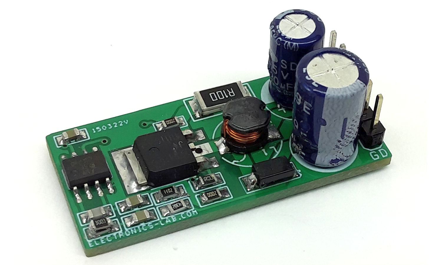
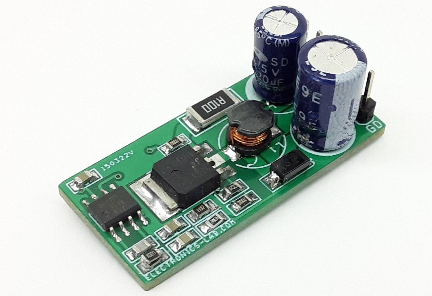
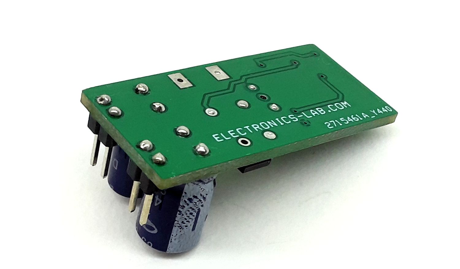
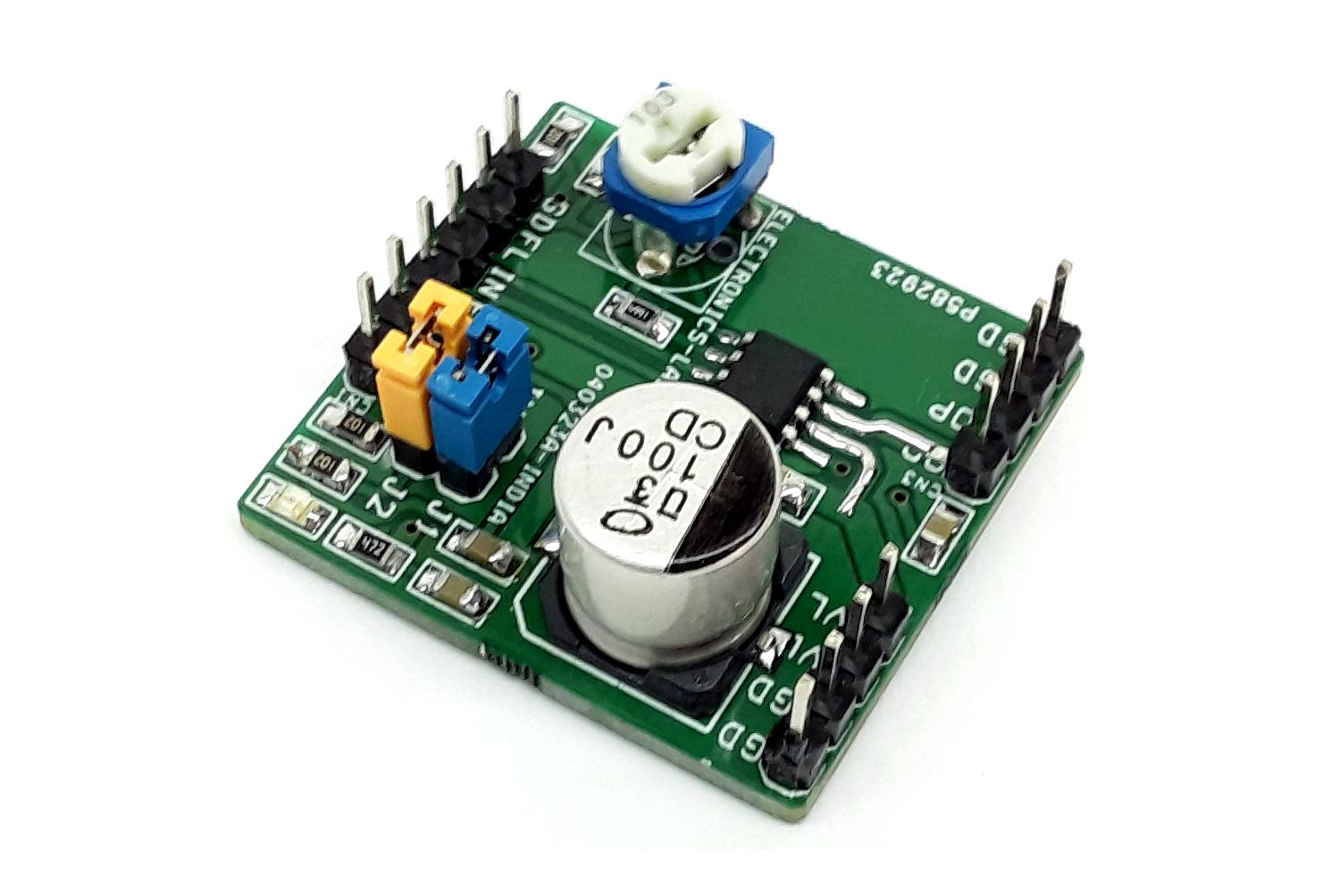
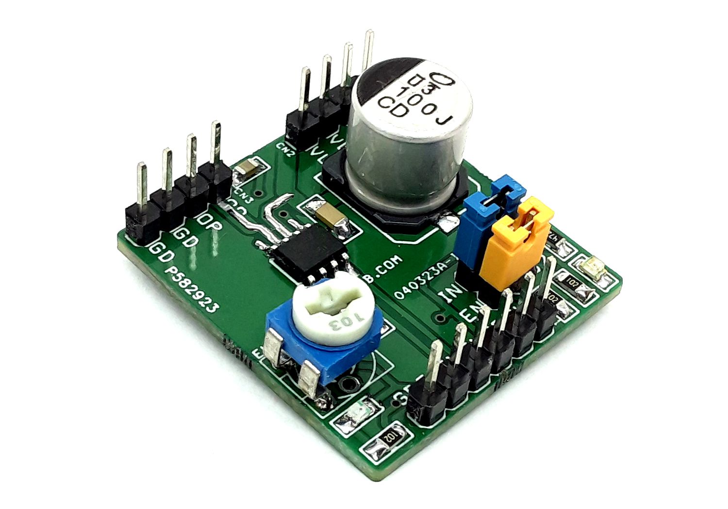
This is a low-cost boost converter that converts a 3.3V input to 5V at 250mA load current. The LM2578A chip is used to build this project. The LM2578A is a switching regulator which can easily be set up for such DC-to-DC voltage conversion circuits as the buck, boost and inverting configurations. In this board, the IC is configured as a boost converter. The operating frequency is 50Khz.
Features
Input Voltage 3.3V
Output Voltage 5V DC (+/-5%)
Output Current 250mA
Efficiency Approx 80%
Current Limit 2A
Operating Frequency 50Khz
Thermal Shutdown
PCB Dimensions 38.58 x 17.94mm
Connections
CN1: Pin 1 = 3.3V DC Input, Pin 2 = GND
CN2: Pin 1 = 5V DC Output, Pin 2 = GND
The boost or step-up converter converts a DC voltage to a higher DC voltage. When the switch software is turned on, energy is stored in the inductor L and the inductor current iL ramps up at a slope determined by the input voltage. Diode D is off during this period. Once the switch, SW, turns off, diode D starts to conduct and the energy stored in the inductor is released to the load. Current in the inductor ramps down at a slope determined by the difference between the input and output voltages.
The LM2578A is a switching regulator which can easily be set up for such DC-to-DC voltage conversion circuits as the buck, boost and inverting configurations. The LM2578A features a unique comparator input stage which not only has separate pins for both the inverting and non-inverting inputs but also provides an internal 1.0V reference to each input, thereby simplifying circuit design and p.c. board layout. The output can switch up to 750 mA and has output pins for its collector and emitter to promote design flexibility. An external current limit terminal may be referenced to either the ground or the Vin terminal, depending upon the application. In addition, the LM2578A has an onboard oscillator, which sets the switching frequency with a single external capacitor from <1 Hz to 100 kHz (typical).
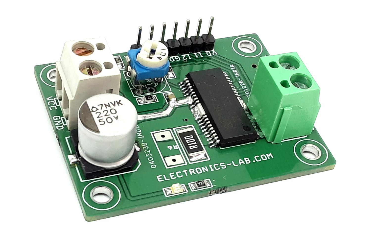
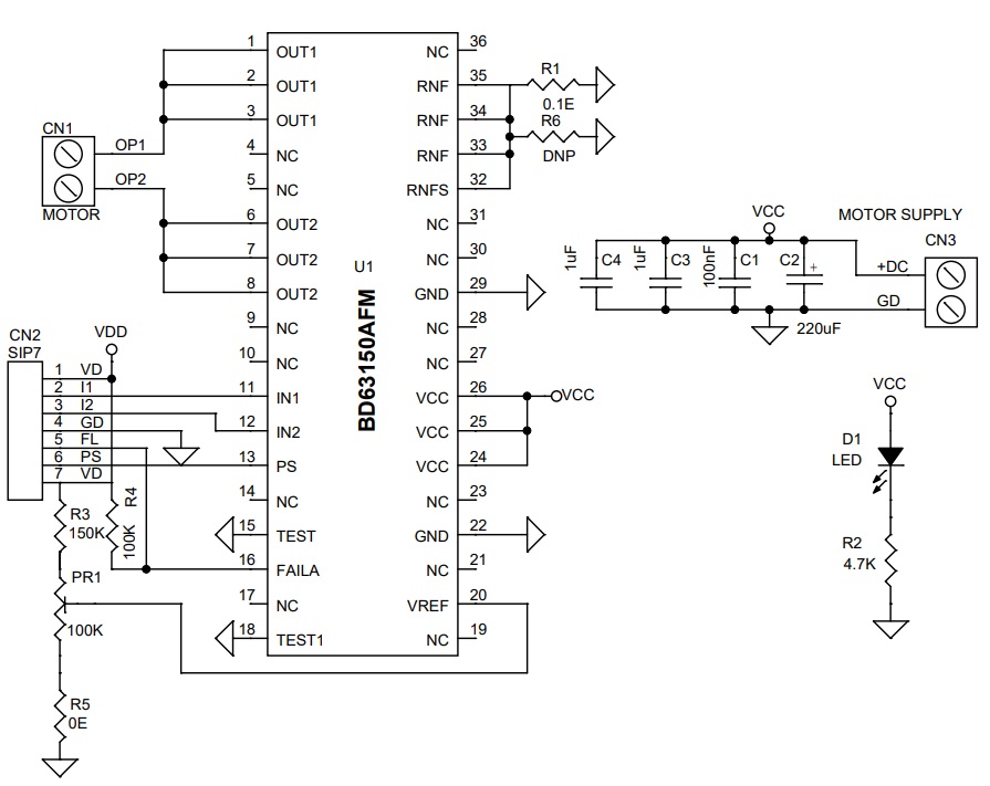
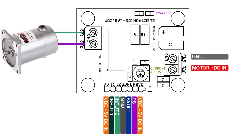
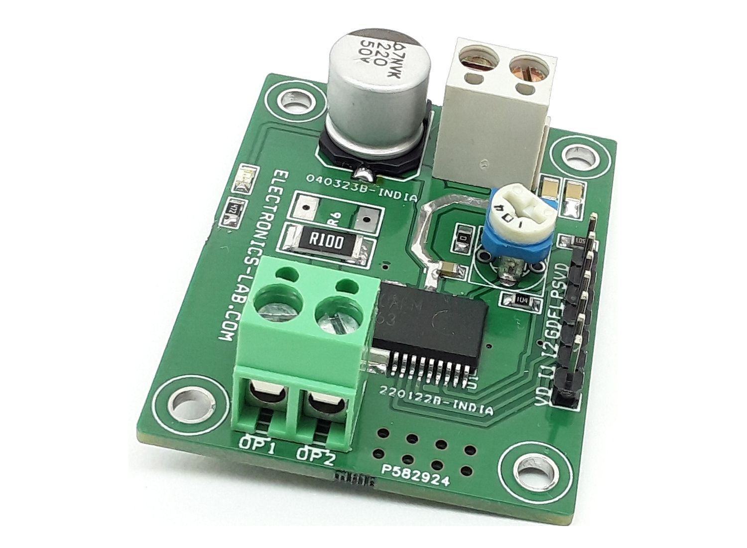
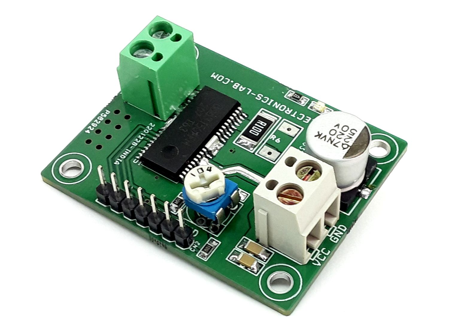
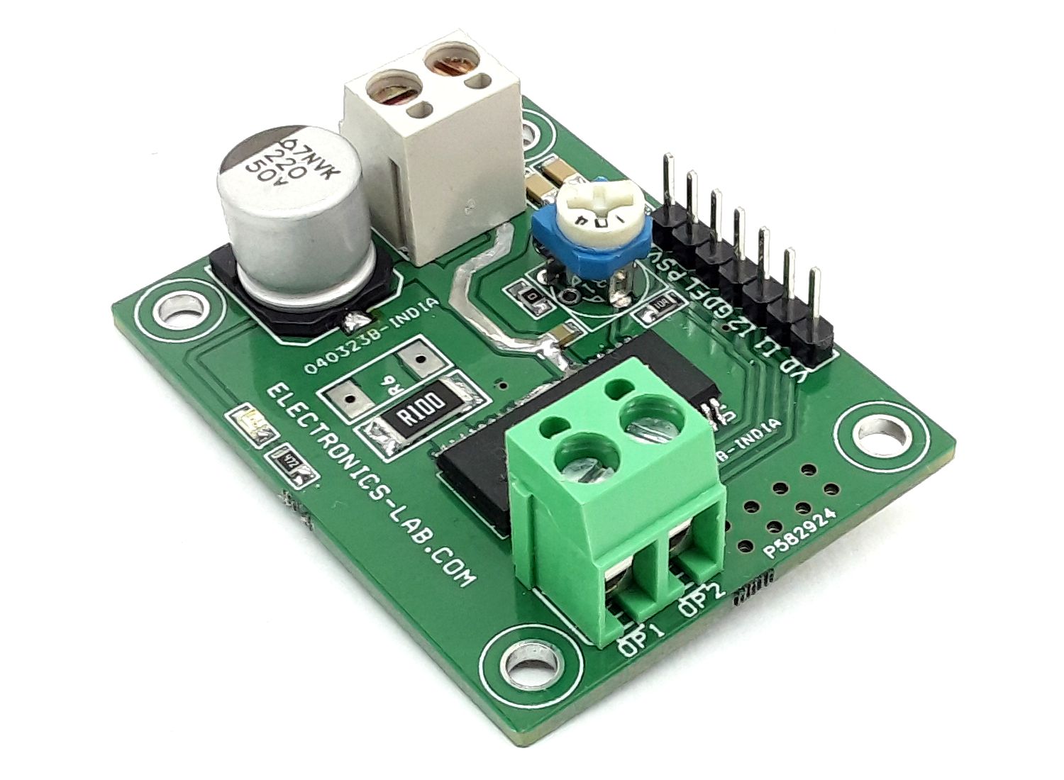
This is a powerful yet small-size and low-profile brushed DC motor drive system, with key features like adjustable constant current control, direction control, brake controls, Alert output, PWM for speed control, etc. The BD63150AFM chip is the heart of the project which is one H-bridge motor driver for DC brush motors. This board enables low power consumption by direct PWM or PWM constant current control. Built-in protection circuits in this IC are present. It is possible to output an abnormal detection signal for Wired-OR that notifies each protection circuit operation, and this contributes to the high reliability of this board.
Constant Current Mode or Direct PWM Mode Selection
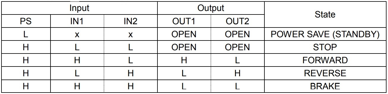
Constant Current Mode: By default, this project works in constant current mode. Constant current can be set using Trimmer Potentiometer PR1. Use Input1 and Input2 of CN2 to control Motor Forward, Reverse, and Brake. Please refer to Table 1 for input logic.
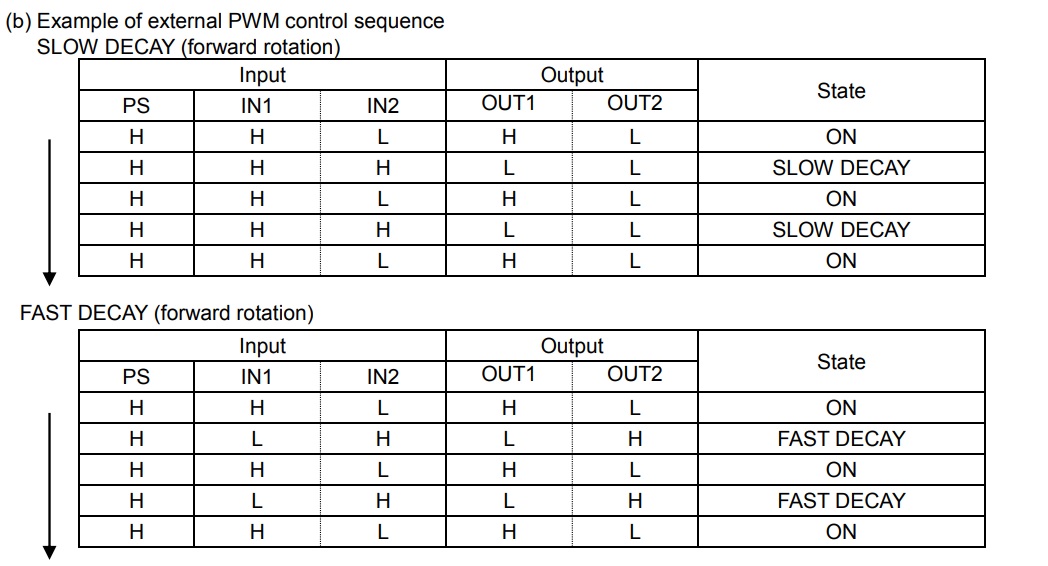
PWM Mode: Replace resistor R1 with 0 Ohms. Adjust the PR1 trimmer potentiometer to 1 to 2V. Use Input1 and Input 2 as external PWM/Logic Input with Maximum Allowable PWM frequency 100Khz. Refer to Table 4 for the input signals diagram.
Note: Use a fan for full load capacity.
Features
Single Power Supply Input Range 8 to 46V DC (rated voltage of 50V)
Rated Output Current (peak): 5.0A(6.0A)
Low ON-Resistance DMOS Output
Forward, Reverse, Brake, Open Function
Power Save Function
External PWM Control – PWM Control Mode
PWM Constant Current Control Adjustable (current limit function)
Built-in Spike Noise Cancel Function (external noise filter is unnecessary)
Built-in Logic Input Pull-down Resistor
Cross-conduction Prevention Circuit
Output Detection Signal during Abnormal states (Wired-OR)
Thermal Shutdown Circuit (TSD)
Over-current Protection Circuit (OCP)
Under Voltage Lock out Circuit (UVLO)
Over Voltage Lock out Circuit (OVLO)
Ghost Supply Prevention (protects against malfunction when power supply is disconnected)
PCB Dimensions 48.10 x 37.62mm
Four Mounting Holes 3mm each
Inputs and Outputs CN2
Pin1: VDD 5V DC @ 10-20mA- Input
Pin2: Input 1 PWM Input or Logic High/Low input Constant Current Mode
Pin3: Input 1 PWM Input or Logic High/Low input Constant Current Mode
Pin4: GND
Pin5: Fault
Pin5: PS
Pin7: VDD 5V DC @ 10-20mA- Input
CN3 Motor Supply Input
Pin1: +DC 8 to 46V Motor Supply
Pin2: GND
CN4 DC Bushed Motor
Pin1: Motor 1 (Output1)
Pin2: Motor 2 (Output2)
Trimmer Potentiometer PR1
Constant Current Adjust
LED D1: Power LED
PS/ Power Save Pin Low=Power Same Mode Standby Mode, High=Active
PS can put the circuit into a standby state and make motor outputs OPEN. Be careful because there is a delay of 40μs(Max), as PS=L→H, until it is returned from standby state to normal state and the motor output becomes ACTIVE.
Input1 and Input2 (Refer Table-1)
IN1, IN2/ H-Bridge Control Pin It decides the output logic for the H-bridge
FAILA/ Fault Signal Output Pin (Refer Table -2)
FAILA outputs an abnormality detection signal when Over-Current Protection (OCP) or Thermal Shutdown (TSD) operates. Even if Under Voltage Lock Out (UVLO) or Over Voltage Lock Out (OVLO) operates, the FAILA signal doesn’t turn an abnormality detection signal (i.e., high). This signal can be connected to the microcomputer and the system can be shut down. This pin is an open drain type, and a Pull-up resistor R4 is used. Normal output is High, this pin goes low when a fault condition arises.
Thermal Shutdown (TSD)
This IC has a built-in Thermal Shutdown circuit for thermal protection. When the IC’s chip temperature rises 175°C (Typ) or more, the motor output becomes OPEN. Also, when the temperature returns to 150°C (Typ) or less, it automatically returns to normal operation. However, even when TSD is in operation, if heat is continued to be applied externally, heat overdrive can lead to destruction.
Over-Current Protection (OCP)
This IC has a built-in Over-Current Protection circuit as a provision against destruction when the motor outputs are shorted to each other or VCC-motor output or motor output-GND is shorted. This circuit latches the motor output to OPEN condition when the regulated current flows for 4μs (Typ). It returns with power reactivation or a reset of the PS pin. The over-current protection circuit aims to prevent the destruction of the IC only from abnormal situations such as when motor output is shorted and it is not meant to be used as protection or security for the device. Therefore, the device should not be designed to make use of the function of this circuit. After OCP operation, if abnormal situations continue and are returned by power reactivation or reset of the PS pin happens repeatedly, then OCP operates constantly. The IC may generate heat or otherwise deteriorate. When the L value of the wiring is great due to the wiring being long, if the output pin voltage jumps up and the absolute maximum values may be exceeded after the overcurrent has flowed, there is a possibility of destruction. Also when the current which is the output current rating or more and the OCP detection current or less flows, the IC can heat up to Tjmax=150°C or more and can deteriorate, so the current which exceeds the output rating should not be applied.
Under Voltage Lock Out (UVLO)
This IC has a built-in Under Voltage Lock Out function to prevent false operations such as IC output during power supply under voltage. When the applied voltage to the VCC pin goes 5V (Typ) or less, the motor output is set to OPEN. This switching voltage has a 1V (Typ) hysteresis to prevent false operation by noise etc. Be aware that this protection circuit does not operate during power save mode.
Over Voltage Lock Out (OVLO)
This IC has a built-in Over Voltage Lock Out function to protect the IC output and the motor during power supply overvoltage. When the applied voltage to the VCC pin goes 52V (Typ) or more, the motor output is set to OPEN. This switching voltage has a 1V (Typ) hysteresis and a 4μs (Typ) mask time to prevent false operation by noise etc. Although this over-voltage-locked-out circuit is built-in, there is a possibility of destruction if the absolute maximum value for power supply voltage is exceeded. Therefore, the absolute maximum value should not be exceeded. Be aware that this protection circuit does not operate during power save mode.
Ghost Supply Prevention (protects against malfunction when the power supply is disconnected)
If a control signal (IN1, IN2, PS, and VREF) is applied when there is no power supplied to the IC, there is a function that prevents a malfunction where voltage is supplied to the power supply of this IC or other IC in the set via the electrostatic destruction prevention diode from these input pins to the VCC. Therefore, there is no malfunction in the circuit even when voltage is supplied to these input pins while there is no power supply.
PWM Constant Current Control (refer to Table 3)
This function can limit the peak current such as switching current in driving the DC brush motor.
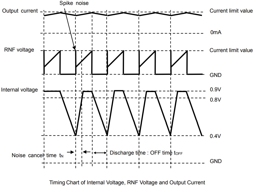
Current Control Operation The output current increases due to the output transistor being turned on. When the voltage on the RNF pin, the output current is converted due to connecting the external resistance to the RNF pin, reaches the voltage value set by the VREF input voltage, and the current limit comparator engages and enters the current decay mode. Thereafter the output turned on again after a period of time determined the CR pin. The process repeats itself constantly.
Blank Time (Fixed in Internal Circuit) In order to avoid misdetection of the current detection comparator due to RNF spikes that occur when the output turns ON, the internal voltage between 0.4V and 0.8V is provided as minimum ON time (tONMIN 1.5µs Typ). During this time, the current detection is disabled after the output transistor is turned on. This allows for the constant-current drive without the need for an external filter.
Internal Timer (Fixed in Internal Circuit) Repeat charging and discharging between 0.4V to 0.9V internal voltage determined by IC internal circuit. When internal voltage is changed charge from discharge, the output is then ON from the current decay mode.
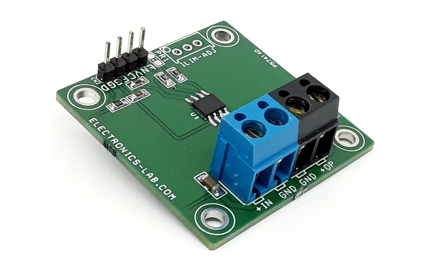
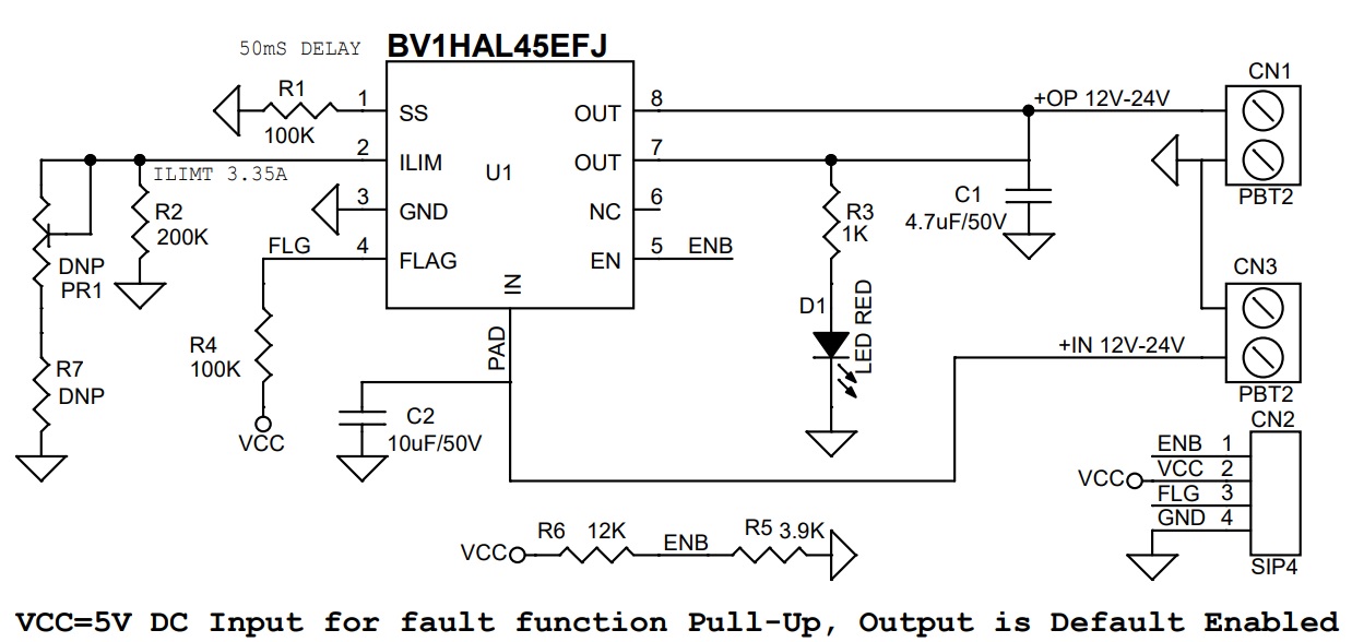
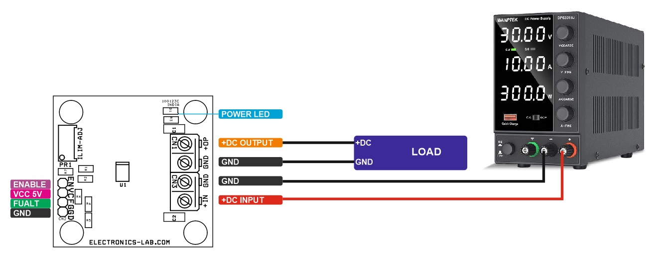
This over-current latch load switch provides over-current protection, thermal shutdown protection, soft-start function, and low power OFF function. The Overcurrent protection function is activated when the load is shorted. This protection function is effective in preventing damage due to sudden and unexpected incidents. It is also equipped with an error flag notification pin which indicates thermal shutdown and over-current condition. The project can help to protect the connected device from overcurrent, monitoring of various power lines, and power management. The board operates from 12V DC to 24V DC. The power LED indicates the output. Screw terminals provided for an easy connection of input and output supply. For the Fault function, additional 5V VCC DC input is required, otherwise, the VCC is not required. The circuit is normally enabled, and you can connect enable pin to GND to disable the output. Output is latching type; power is OFF when a fault condition occurs and sequence can be reversed with power OFF or Disable/Enable Pin.
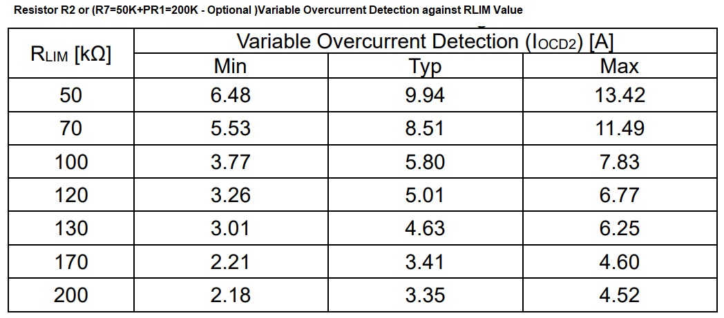
Note1: Default over current threshold = 3.35A, this can be increased by changing the value of resistor R2 (Between 3.35A to 10A/ R2=200K Ohms to 50K Ohms), Optional Onboard multiturn potentiometer is provided for easy adjustment of the current range, Use R7=50K, PR1=200K Ohms- Bourns Inc Type 3296, and do not install R2 in this case.
Note2: PCB has a small thermal area for power dissipation for current loads up to 3.35A, it is important to use Fan when a higher current threshold is selected.
Features
Operating Supply 12V DC to 24V
Operating Current 3mA + 5mA LED = 8mA Approx
Load Current 3Amps
Output Load Voltage 12V-24V DC
Output On Resistance 45mOhms
Over Current Threshold 3.35A (Adjustable 3.35A to 10Amps, Read Note)
Over Current Protection Function (Latch OFF)
Thermal Shutdown Protection Function (TSD)
Low Voltage Output OFF Function (UVLO) Threshold 6V
Standby Current 5uA + LED Current
Operating Temperature -40C to +85C
Error Flag Notification Output, Normally High ( VCC=5V)
PCB Dimensions 40.64 x 39.69mm
4 X 3MM Mounting Holes
Connections and Other Details
CN1: Pin 1 = +12V to +24V DC Output, Pin 2 = GND
CN2: Pin 1 = Enable (Default Enabled, Connect to GND = Disable), Pin 2 = VCC 5V DC Flag Pull-Up Supply, Pin 3 = Flag Output (Default High, Low= When Fault Condition Occurs), Pin 4 = GND
CN3: Pin 1 = +12V to +24V DC Input, Pin 2 = GND
D1: Output Power LED
R2: Current Limit Adjust, Refer Figure
PR1 + R7: Optional for Adjustable Current Limit
R1: Soft Start Delay 50mS (Refer Figure to change Delay)
Thermal Shutdown Function
(Thermal Shutdown Detection TTSD, Thermal Shutdown Hysteresis TTSDHYS) This IC has a built-in TSD function. When the temperature of the IC reaches Thermal Shutdown Detection (TTSD) = 175 °C (Typ) or more, the output is turned off, and the FLAG outputs Low. Hysteresis (TTSDHYS) is installed for thermal shutdown function, and output automatically returns to normal when chip temperature becomes 160 °C (Typ) or less. The condition for Latch-Off is when Variable Overcurrent Detection (IOCD2) is reached and the temperature of IC reaches Thermal Shutdown Detection (TTSD) = 175 °C (Typ) or more. The condition for Latch-off Release is the switching of EN voltage (VEN) or IN voltage (VIN).
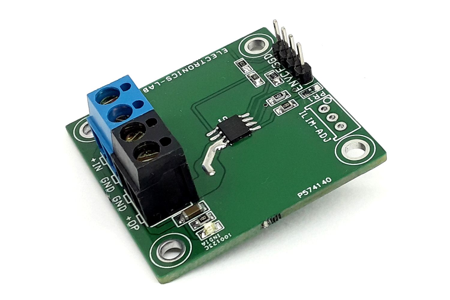
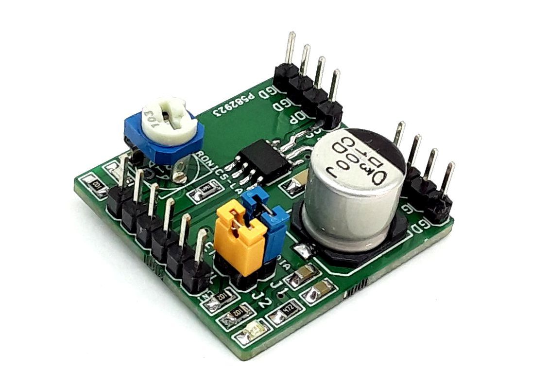
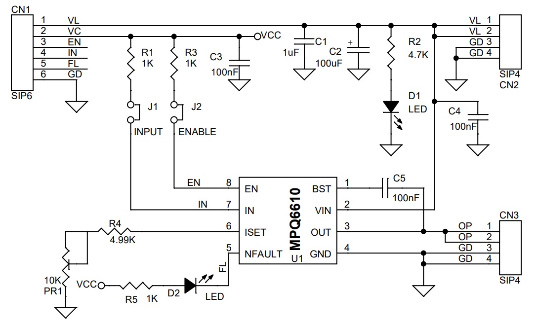
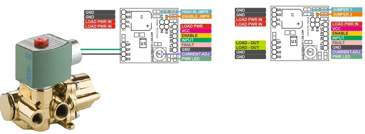
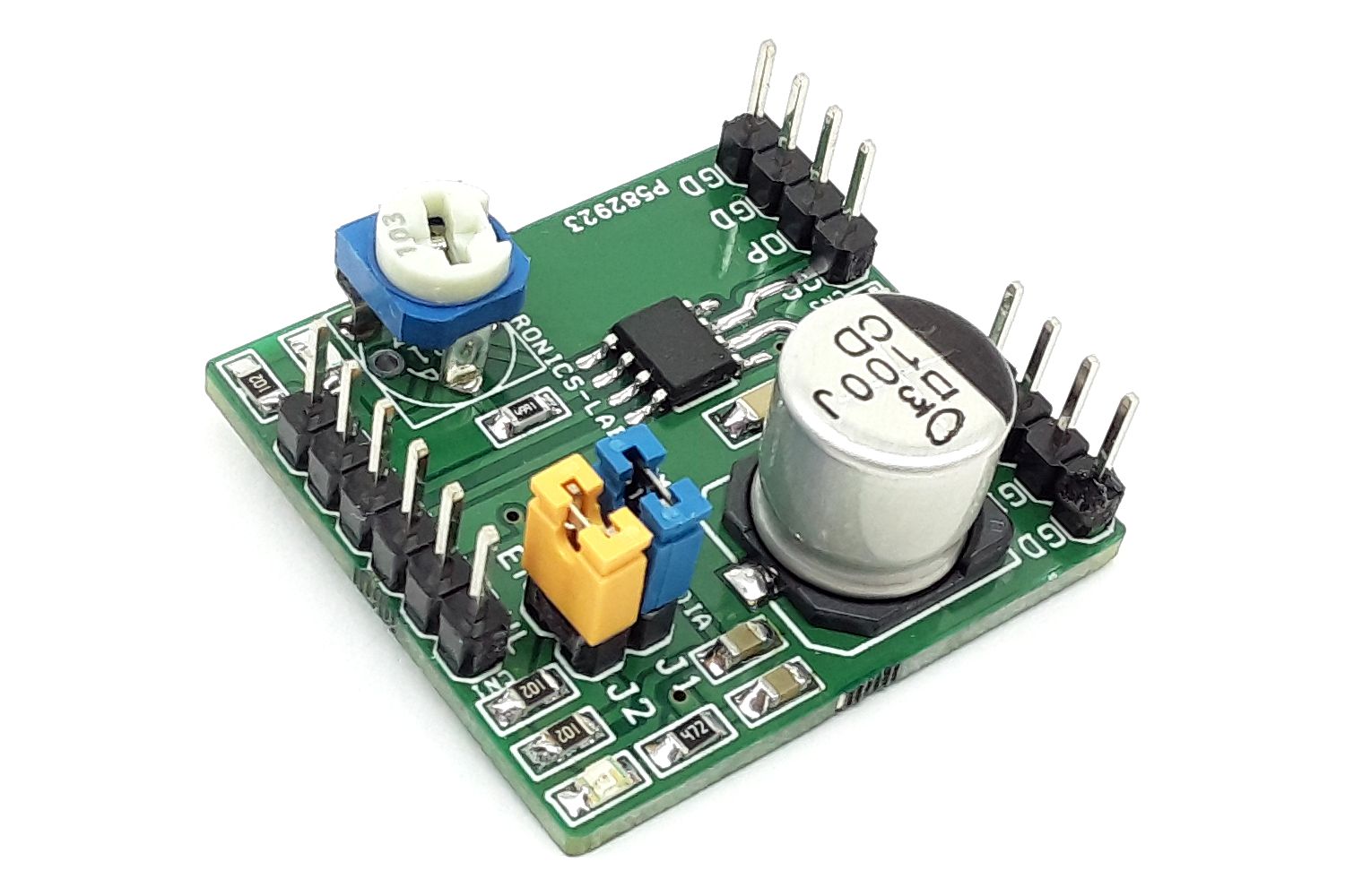
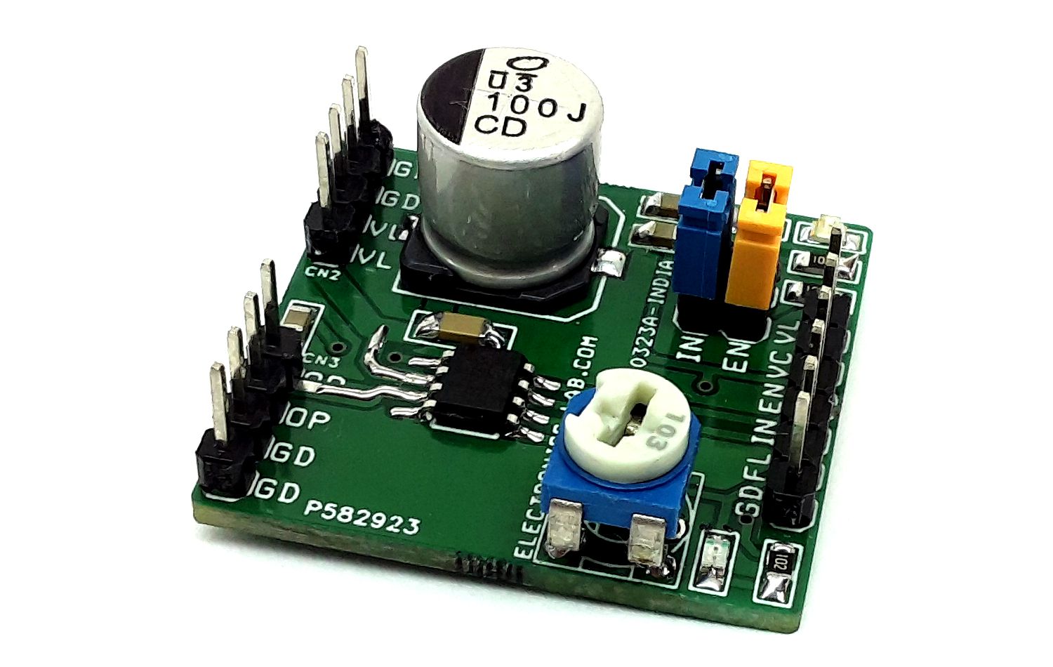
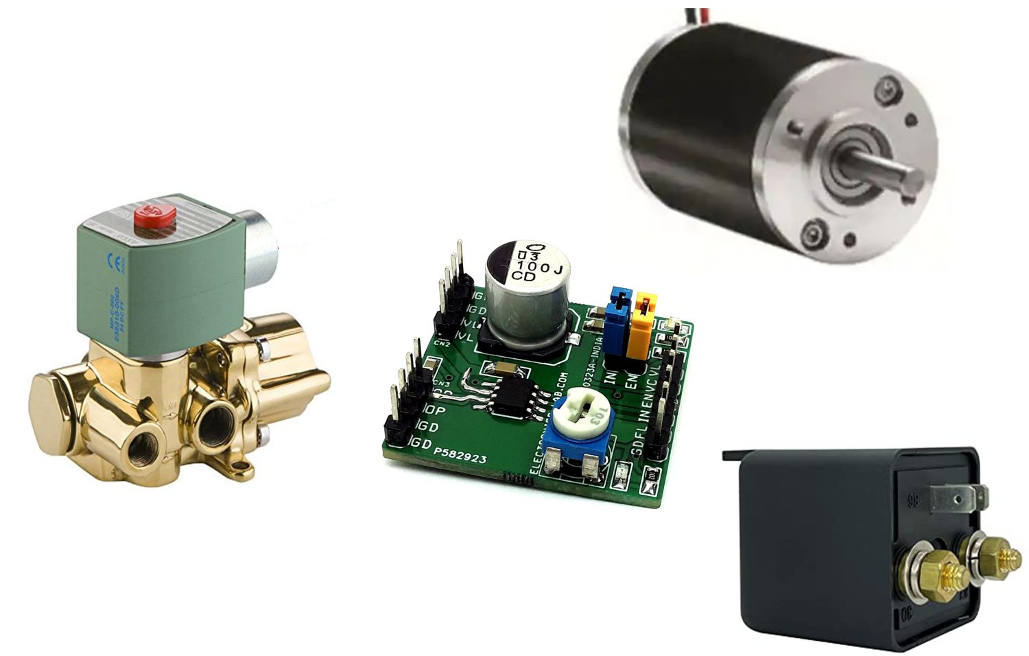
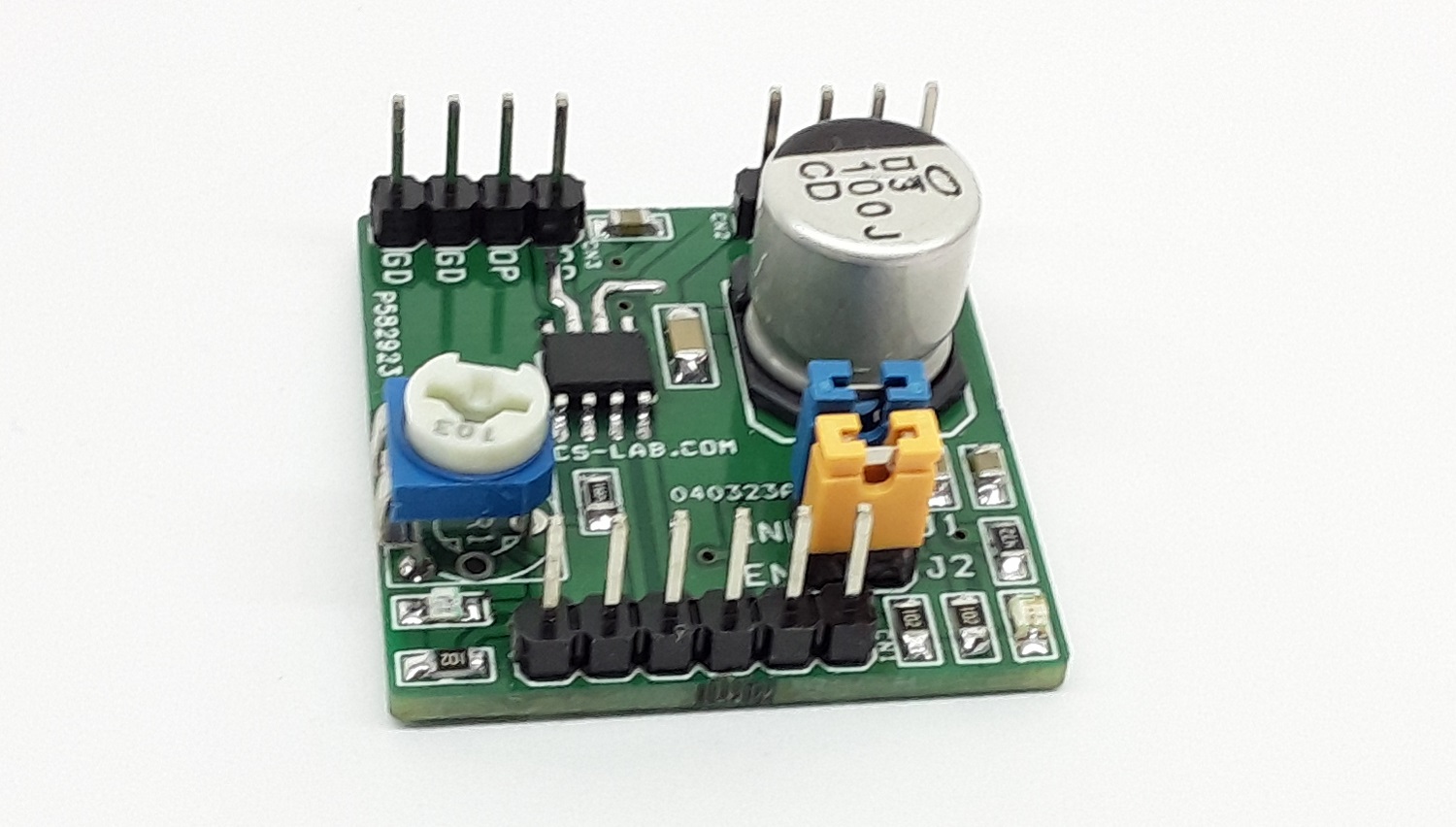
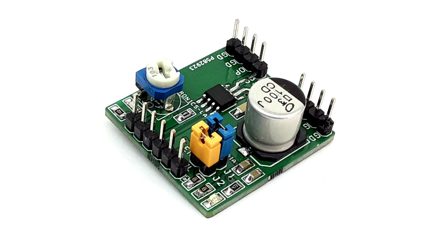
This Half-bridge module provides current measurement and regulation features for various loads. The module can be used to drive solenoids, Relays, Valves, DC-DC converters, Brushed DC motors, or other loads. It can operate from a 5V to 55V supply voltage and can deliver up to 3A of output current (depending on ambient temperature). Cycle-by-cycle current regulation, current limiting is adjustable using PR1 trimmer pot. Internal diagnostic and protection features include open-load detection, over-current protection (OCP), under-voltage lockout (UVLO), and thermal shutdown. The overcurrent limit is set to 3A and the retry time is 1.6mS. Solenoids can be controlled ON/OFF using Jumper J1. Use the PWM signal at the input pin for DC motor speed control.
Jumper J1 = Internal Enable, Don’t Use this Jumper In case External Enable Input CN1 Pin 3 Required
Jumper J2 = Output Direct Triger, Don’t Use this Jumper In Case External PWM Input CN1 Pin 4 Required
D1: Power LED
D2: Fault LED, Glow if a fault condition (e.g. over-current protection [OCP], over-temperature protection [OTP], or open load) occurs
PR1: Trimmer Potentiometer to Set the Current Limit
Input Logic: Each MOSFET in the MPQ6610 is controlled independently using the IN and EN pins
Enable Low, In Low Output Hi-Z
Enable Low, In High Output Hi-Z
Enable High, In Low Output Low
Enable High, In High Output High
The input pins are designed such that they can be driven with a logic level voltage even when the main power to the device is inactive.
Current-Sense
The current flowing in the low-side MOSFET (LS-FET) or high-side MOSFET (HS-FET) is sensed with an internal current-sense circuit. A voltage that is proportional to the output current is sourced on the ISET pin. The ISET pin voltage scaling is set by a resistor connected between the ISET pin and ground. For 1A of output current, 100µA of current is sourced into the resistor connected to ISET. For example, if a 10kΩ resistor is connected between ISET and ground, the output voltage on the ISET pin is 1V/A of output current. The current is sensed anytime that either the LS-FET or HS-FET is on.
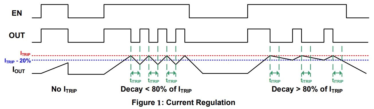
Current Limit and Regulation
The current in the output is limited using constant-off-time (COT) pulse-width modulation (PWM) control circuitry. Figure 1 shows the device’s current regulation system, described below:
First, a MOSFET turns on and drives current through the load.
The current increases in the load, which is then sensed by the internal current-sense circuit.
If the load current reaches the current trip threshold, the output changes its state (if it was driving high, it goes low; if it was driving low, it goes high).
If the load current has fallen at 80% of the current limit threshold after a fixed off time (tITRIP), the original MOSFET is re-enabled. Then the cycle repeats.
If the current is still above this level, the off time is extended until the current falls to 80% of the current limit threshold.
The current limit threshold is reached when the ISET pin reaches 1.5V. For example, with a 10kΩ resistor (R4 + PR1) connected from ISET to ground, the ISET pin voltage is 1V/A of output current. Therefore, when the current reaches 1.5A, the ISET pin voltage reaches 1.5V, and a current trip occurs.
Blanking Time
There is often a current spike while the MOSFET turns on, which can be caused by the body diode’s reverse recovery current or by the shunt capacitance of the load. This current spike requires filtering to prevent it from erroneously shutting down the enabled MOSFET. An internal fixed blanking time (tBLANK) blanks the output of the current-sense comparator when the output is switched. This blanking time also sets the minimum time for which the output remains high or low after the input has changed.
Protection and Diagnostic Functions
The Module has a FAULT pin, which is driven active low if any of the protection circuits are activated. These fault conditions include over-current (OC) and over-temperature protection (OTP), as well as open-load detection. FAULT is not driven low if a current limit trip occurs. FAULT is an open-drain output, and requires an external pull-up resistor with LED. When the fault condition is removed, the FAULT pin is pulled inactive high by the pull up resistor and LED.
Over-Current Protection (OCP)
If the current through any MOSFET of the chip exceeds the over-current (OC) threshold for longer than the over-current deglitch time, an over-current fault is triggered. If an OC fault occurs, the state of the output is reversed until the current approaches 0A. Then both internal MOSFETs of chip are disabled, and the FAULT pin is driven low. The driver remains disabled for about 1.6ms, then is automatically re-enabled.
Open-Load Detection
When the output is in a high-impedance state (EN = 0), the internal circuits pull the OUT pin to VIN / 2 by a weak current. If a load is connected between OUT and ground, then the load pulls the OUT pin close to ground. If a load is connected to VIN, then OUT is pulled close to the value on VIN. If the voltage on OUT (VOUT) is almost VIN / 2, an open-load condition is detected, and the nFAULT pin is driven active low. The fault is cleared when EN is made active.
Input Under-Voltage Lockout (UVLO) Protection
If the voltage on VIN (VIN) falls below the under-voltage lockout (UVLO) threshold at any time, all circuitry in the device is disabled and the internal logic is reset. Once VIN exceeds the UVLO threshold, the module resumes normal operation.
Over-Voltage Protection (OVP)
If VIN exceeds the over-voltage protection (OVP) threshold, the device is disabled. Once VIN falls below the OVP threshold, the module resumes normal operation.
Thermal Shutdown
If the die temperature exceeds its safe limits, all MOSFETs in the H-bridge are disabled, and the FAULT pin goes low. Once the die temperature drops to a safe level, the device automatically resumes normal operation.

 With a strong ESP32-S3 chip, 2.4GHz Wi-Fi compatibility, and Bluetooth 5 (LE), this handheld terminal is built on the powerful ESP32 controller which offers enhanced computing and processing capabilities for IoT terminal applications. The ESP32-S3-N16RB module can lead to a variety of interfaces due to its scalability. It incorporates a MEMS microphone, camera interface, and buzzer function in addition to Crowtail’s digital port, analog port, UART, and IIC interface.