Espressif released the ESP-SR speech recognition library to support various ESP32 modules

Espressif ESP-SR Speech Recognition

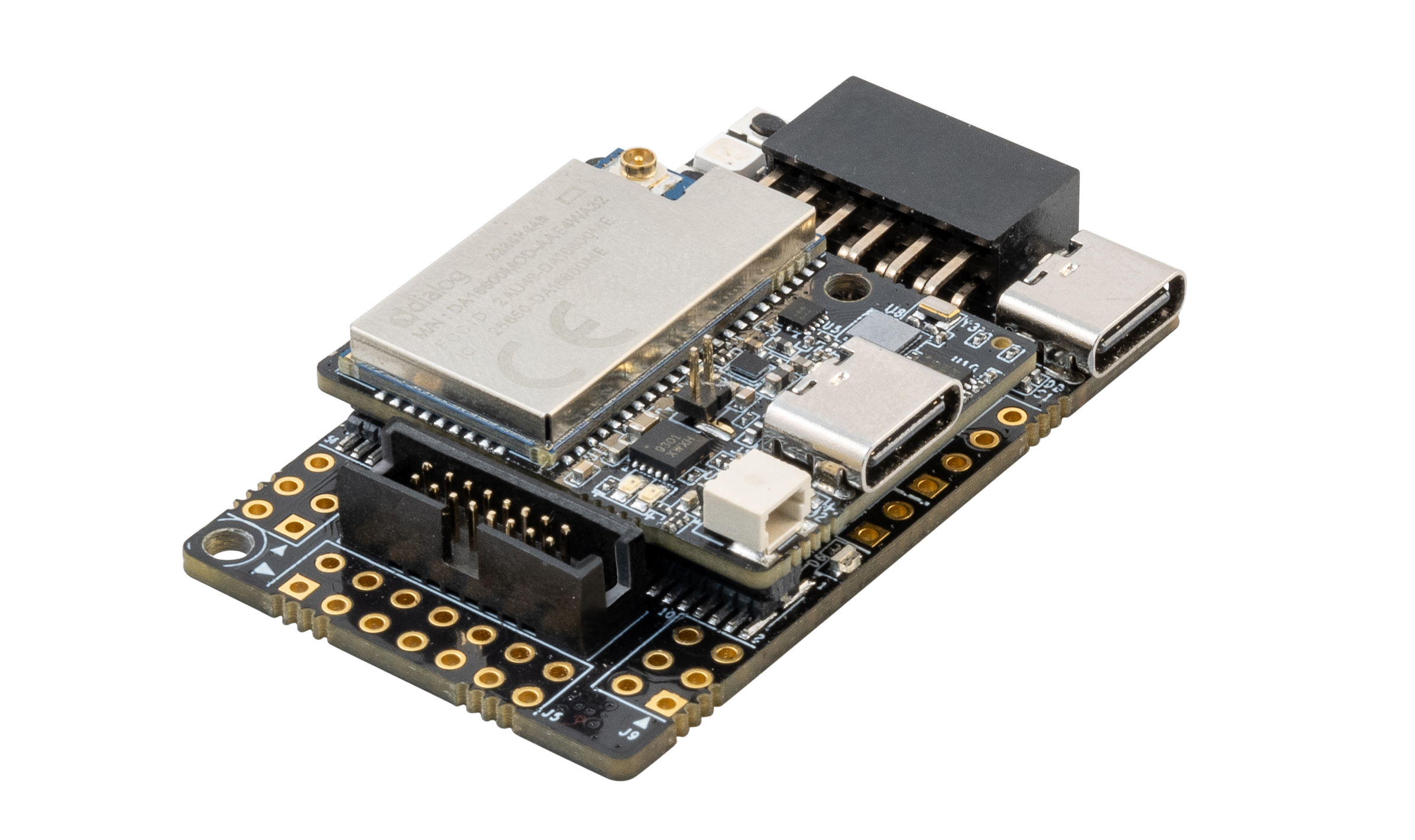
Espressif has released the ESP-SR speech recognition framework that helps the developer to build AI speech applications based on the ESP32 or ESP32-S3 modules. The ESP-SR framework includes four modules– audio front-end (AFR), wake word engine (WakeNet), speech command word recognition (MultiNet), and speech synthesis (for the Chinese language).

  • Audio Front-End: Espressif’s audio front-end algorithms are designed to enhance the accuracy and robustness of voice recognition systems in noisy environments. They apply various digital signal processing techniques to the audio signal, such as noise suppression, acoustic echo cancellation, blind source separation, and voice activity detection.

Espressif’s AEC algorithm supports up to two microphones, meaning it can effectively remove the echo from the microphone input signal for devices with two microphones. This can help improve the performance of speech recognition systems, as the removal of echo can result in cleaner and more accurate speech signals for processing. Espressif’s NS algorithm supports single-channel processing, which means it can suppress non-human noise in single-channel audio.

  • Wake Word Engine: Espressif’s wake word engine, WakeNet, is a specialized software designed to provide users with a high-performance, low-memory footprint wake word detection algorithm. WakeNet has been specifically optimized for use with Espressif’s ESP32-S3 series of chips, providing developers with a reliable and efficient way to add wake word detection to their products.

Espressif has provided an official wake word detection model, including wake words such as “Hi, Lexin” and “Hi, ESP,” to the public for free. This enables developers to quickly and easily add wake word detection functionality to their products without creating their own model. However, Espressif also allows customized wake words, enabling developers to create unique ones to suit their specific product or application needs.

  • Speech Command Recognition: Espressif’s speech command recognition model, MultiNet, is designed to provide a flexible off-line speech command recognition model. MultiNet enables developers to add custom speech commands to their products without the need to train the model from scratch, making the process much simpler and more efficient.

The flexibility of MultiNet allows developers to add their own custom speech commands to their products. This eliminates the need to train the model again, which can be time-consuming. Developers can simply add custom commands, and MultiNet will recognize and respond to them accordingly.

DC UPS solution UPSI-2406 for compact system integration

Emergency power supply protects 24V industrial and medical applications

The new DC UPS solution UPSI-2406 + battery pack BP-LFP-1325S can be flexibly integrated into a wide range of applications to protect sensitive or safety-relevant systems in case of power failure, voltage dip or flicker. The 24V DC emergency power supply ensures fail-safe operation in an emergency and prevents data loss.

All advantages at a glance

  • Integratable 24VDC emergency power supply
  • Ideal for long bridging times: 600 min (2W) – 25 min (70W) – 10 min (150W)
  • 10-year battery pack LiFePO4
  • USB & RS232 interface and relay contact
  • UPS management software included
  • Shutdown & Reboot function for IPC
  • Extended temperature range -20 to +55°C
  • IEC 62133-2 safety approval
  • UN 38.3 Transport certificate

The LiFePO4 energy storage (lithium iron phosphate) with 33 Wh convinces in safety-relevant applications with a particularly stable battery chemistry, a long service life of at least ten years and more than 6,000 full charge and discharge cycles. Bicker Elektronik deliberately relies on the particularly safe lithium iron phosphate chemistry for all high-performance battery packs, which makes thermal runaway almost impossible.

The new UPS management software ‘UPScom’ with cross-platform technology and intuitive user interface offers extensive functions for monitoring, parameterisation and messenger services.

Intuitive user interface and extensive functionality

The software ‘UPScom’ allows the connected devices to be shut down and switched off in a controlled manner during a power failure in order to avoid data loss or damage. The responsive WEB UI is called up in a web browser to set and pre-program all parameters of the DC UPS system and for real-time monitoring with state-of-charge indicator. The adjustable parameters include, among other things, load sensor (mA), shutdown delay, maximum backup time, minimum charge capacity before system start, notifications by email.

Cross platform technology

‘UPScom’ uses the new WebAssembly (WASM) architecture, which runs in most current web browsers. ‘UPScom’ runs on x86 compatible systems and also on most ARM-64 based systems under Microsoft® Windows and various Linux distributions.

Secure Shutdown & Reboot function for IPC systems

In the event of a “power failure”, the UPS signals the failure of the supply voltage via the integrated USB or RS232 interface, so that a controlled shutdown of the computer system is initiated and valuable data is saved. A script (batch) can also be executed before the system is shut down in order to process your own application-relevant processes. The integrated reboot function of the DC UPS automatically restarts the supplied IPC after the supply voltage returns, without the need for time-consuming on-site intervention by a service employee, e.g. in the case of completely self-sufficient computer systems at inaccessible locations.

Email messenger service

‘UPScom’ can be used for various events such as loss of connection to the UPS, system shutdown or power failure. These preventative measures can reduce or eliminate downtime.

Avnet launches RASynBoard with onboard machine learning capabilities

Avne RASynBoard Development Kit

The technology solutions company, Avnet, has released a new development kit called RASynBoard. This kit is specifically created to assist both hardware and software engineers in seamlessly incorporating edge artificial intelligence (AI) functions into their products, with the aim of speeding up the integration process.

The RASynBoard, developed jointly with Renesas, Syntiant, and TDK, incorporates a Renesas microcontroller and Syntiant Neural Decision Processor (NDP), as well as TDK sensors, to create an ultra-low-power edge AI platform. This compact kit is suitable for use as an additional sensor module for existing products or can be adapted and integrated into more comprehensive systems to meet more demanding sensing requirements.

The RASynBoard module is composed of two main domains: an AI processor that is always active and contains built-in sensors and a controller based on an MCU that has a low-power Wi-Fi and Bluetooth wireless module. The AI processor utilized on the RASynBoard is the Syntiant NDP120 Neural Decision Processor, while the MCU controller is the Renesas RA6M4.

Avnet RASynBoard front-view

The Core Board of RASynBoard contains the Renesas DA16600 module, which combines Wi-Fi and Bluetooth capabilities, and two TDK sensors: the ICM-42670-P 6-axis IMU and the MMICT5838 PDM digital microphone. The AI processing system can activate the MCU controller when it detects an AI-triggered “event,” allowing the MCU system to act or send a wireless notification before reverting to low-power AI sensing mode. The developers can personalize both the sensors connected to the AI processor and the AI algorithm that runs on the AI processor.

The RASynBoard Development Kit comes with the IO Board, which features built-in debugging and programming capabilities for the RA6M4 MCU, as well as expansion options for both the MCU and NDP120. Additionally, the IO Board is equipped with a micro-SD card interface for the RA6M4 MCU that can be utilized for extra data storage if required. Both Pmod and Click interfaces can be added to the IO Board to provide various sensing or control capabilities.

Avnet has collaborated with Edge Impulse to offer assistance to RASynBoard through the Studio machine learning platform. Avnet’s Vice President of Advanced Applications Group, Jim Beneke, stated, “Our design customization and manufacturing capabilities also allow us to offer production-ready solutions for customers needing a full-turnkey option.”

Avnet is currently accepting pre-orders for the RASynBoard Core Board and IO Board bundle on its website, which costs $99. The delivery of the bundle is anticipated to take place towards the end of the second quarter of 2023.

B&K Precision 9240 Multi-Range DC Power Supplies

B&K Precision 9240 Multi-Range DC Power Supplies provide up to 120W (9240 and 9241) or 200W (9242) of multi-range power in a compact 2U half-rack form factor. These power supplies combine an easy-to-use interface with an advanced list of programming features, battery charge mode, and data logging. The battery charge mode provides configurable fail-safe settings to disable the output when a specified energy, capacity, or time threshold is reached. The 9240 power supplies offer system integrators with LXI-compliant LAN and USB interfaces standard for remote control and programming with a GPIB model option.

The 9240 power supplies feature isolated and floating output with front panel remote sense, thermostatically-controlled fan for quiet operation, and adjustable voltage and current slew rate. These power supplies support Over-Voltage Protection (OVP), Over-Current Protection (OCP), Over-Temperature Protection (OTP), key-lock function, remote inhibit, and voltage fault. The 9240 power supplies are TUVus certified, indicating compliance with Canadian and U.S. National safety standards. These power supplies comply with cTUVus certification, which fulfills CSA and UL safety standards.

Features

  • Isolated and floating output with front panel remote sense
  • Up to 120W or 200W of multi-range power in a compact 2U half-rack form factor
  • Voltage range:
    • 0V to 32V (9240)
    • 0V to 60V (9241 and 9242)
  • Clean output power with less than 1mVRMS of noise
  • Advanced list mode programming with internal storage for 10 list mode programs
  • Battery charge mode with fail-safe conditions
  • Direct data logging to a USB flash drive
  • Thermostatically-controlled fan for quiet operation
  • Adjustable voltage and current slew rate
  • LED test mode for protecting components from inrush currents
  • Digital I/O terminal offers external triggering, voltage fault, and remote inhibit capabilities
  • LabVIEW, IVI-C, and IVI.NET drivers
  • Remote PC control software available
  • Convenient front-panel user calibration
  • cTUVus certification mark fulfills CSA and UL safety standards
  • NISPOM-compliant sanitization to securely restore factory settings

more information: https://www.bkprecision.com/products/power-supplies/9240

Analog Devices Inc. ADTF3175 1-MegaPixel Time-of-Flight Module

Analog Devices ADTF3175 1-MegaPixel Time-of-Flight Module is based on the ADSD3100, a 1-Megapixel CMOS indirect Time-of-Flight (iToF) imager and designed for high-resolution 3D depth sensing and vision systems. The ADTF3175 integrates a lens and optical bandpass filter for the imager, an infrared illumination source containing optics, a laser diode, a laser diode driver and photodetector, flash memory, and power regulators to generate local supply voltages. Fully calibrated at multiple range and resolution modes, the raw image data from the ADTF3175 is processed externally by the host system processor or depth ISP to complete the depth sensing system.

The ADTF3175 image data output interfaces electrically to the host system over a 4-lane mobile industry processor interface (MIPI), Camera Serial Interface 2 (CSI-2) Tx interface. The module programming and operation are controlled through 4-wire SPI and I2C serial interfaces. The Analog Devices ADTF3175 1-MegaPixel Time-of-Flight Module measures 42mm × 31mm × 15.1mm and operates over a -20°C to +65°C temperature range.

Features

  • 1024 × 1024 ToF imager with 3.5µm × 3.5µm pixels
  • 75° × 75° Field of view (FOV)
  • Imager lens subassembly with 940nm bandpass filter
  • Illumination subassembly with eye safety support
  • 4-lane MIPI CSI-2 Tx interface, 1.5Gbps per lane
  • 4-wire SPI and 2-wire I2C serial interfaces
  • NVM (Flash) for the module boot-up sequence
  • Power regulators for the local imager and illumination rails
  • Calibrated modes at 1024 × 1024 and 512 × 512 resolutions
  • 0.4m to 4m depth range (depth noise 15mm maximum, 15% minimum reflectivity, <5klux equivalent sunlight)
  • ±3mm depth accuracy (across full depth range)

more information: https://www.analog.com/en/products/adtf3175.html

Microchip’s MCP9700 and MCP9701 low-power linear active thermistor ICs provide a low-cost solution

Microchip’s low-power MCP9700, MCP9700A, MCP9700B, MCP9701, and MCP9701A analog temperature sensors with linear active thermistor integrated circuit (IC) convert temperature to analog voltage. These sensors have accuracy of ±1°C from +20°C to +70°C (MCP9700B), ±2°C from 0°C to +70°C (MCP9700A and MCP9701A), and ±4°C from 0°C to +70°C (MCP9700 and MCP9701) and consume 6 µA (typical) of operating current. These sensors provide a low-cost solution for applications requiring relative temperature change measurement.

Features

  • Available packages:
    • SC70-5, SOT-23-3, and TO-92-3 (not available with the MCP9700B)
  • Wide temperature measurement range:
    • -40°C to +125°C (extended temperature)
    • -40°C to +150°C (high temperature)
  • Accuracy:
    • ±1°C (max.), +20°C to +70°C (MCP9700B)
    • ±2°C (max.), 0°C to +70°C (MCP9700A and MCP9701A)
    • ±4°C (max.), 0°C to +70°C (MCP9700 and MCP9701)
  • Tiny analog temperature sensor
  • Optimized for analog-to-digital converters (ADCs):
    • 10 mV/°C (typical) (MCP9700, MCP9700A, and MCP9700B)
    • 19.5 mV/°C (typical) (MCP9701 and MCP9701A)
  • Wide operating voltage range:
    • VDD = 2.3 V to 5.5 V (MCP9700, MCP9700A, and MCP9700B)
    • VDD = 3.1 V to 5.5 V (MCP9701 and MCP9701A)
  • Low operating current of 6 µA (typical)
  • Optimized to drive large capacitive loads

more information: https://www.microchip.com/en-us/product/MCP9700A

IT8500G+ Series DC Electronic Load

ITECH’s IT8500G+ series programmable DC electronic load for ATE systems and component testing

ITECH’s IT8500G+ series, with a sampling bandwidth of up to 300 KHz, is a programmable DC electronic load specifically designed for high-precision ripple testing. With the built-in ripple test function, it is easy to measure voltage and current ripple of the DUT. IT8500G+ has as many as eight fast charging protocols built-in, meeting the test requirement of fast charging adapters, power banks, fast charging power banks, and other products. At the same time, it also has other functions like automatic testing, battery discharge testing, dynamic testing, and more, so it can complete most of the performance testing of switching power supplies, batteries, and other products during the development and production stages.

Features

  • Seven operating modes: CC/CV/CR/CW/CR+CC/CV+CC/CR-LED
  • Built-in voltage ripple and current ripple measurement function
  • Dynamic mode up to 20 kHz
  • Measurement resolution up to 0.1 mV/0.1 mA
  • Professional multi-channel mode, which can cascade up to 16 devices to reduce the cost of burn-in testing
  • Battery discharge mode, providing three cut-off conditions of time, voltage, and capacity
  • OPP/OCP test functions, suitable for power module protection function test
  • Automatic test function, widely used in adapter test
  • List function, which can simulate complex current carrier waveforms
  • Current monitoring function, without an expensive current probe, easy to realize current waveform monitoring (0 V to 10 V)
  • Short-circuit mode/measure function

more information: https://www.itechate.com/en/product/dc-electronic-load/IT8500Gplus.html

DRV8317 3-Phase PWM Motor Driver

Texas Instruments’ integrated MOSFET driver is suitable for driving 3-phase motors

Texas Instruments’ DRV8317 3-phase PWM motor driver provides three integrated MOSFET half-bridges for driving 3-phase brushless DC (BLDC) motors with 5 V, 9 V, 12 V, or 18 V DC rails or 2s to 4s batteries. The driver provides integrated 3-phase current sensing, eliminating the need for external sense resistors. The DRV8317 has an integrated LDO that provides a regulated 3.3 V rail that can deliver up to 80 mA for external loads such as microcontrollers (MCUs), logic circuits, hall sensors, and more. The configurable 6x or 3x PWM-control scheme can implement a sensored or sensorless field-oriented control (FOC), sinusoidal control, or trapezoidal control using an external MCU.

The DRV8317 can drive a PWM frequency of up to 200 kHz and is highly configurable through the SPI (DRV8317S) or pins (DRV8317H). The configurable features include PWM mode, slew rate, current-sense gain, and more. The integrated protection features include supply undervoltage lockout (UVLO), overvoltage protection (OVP), charge-pump undervoltage (CPUV), overcurrent protection (OCP), overtemperature warning (OTW), overtemperature shutdown (OTS), and protects the device, motor, and the system against fault events which are indicated by the nFAULT pin.

Features

  • 3-phase BLDC motor driver:
    • Configurable slew rate for EMI mitigation
    • Programmable gain current sensing
    • Supported PWM frequency: up to 200 kHz
    • Integrated shoot-through protection
  • Operating voltage range: 4.5 V to 20 V (24 V abs. max.)
  • High output current capability: 5 A peak-current drive
  • Low on-state resistance MOSFETs: RDS(ON) (HS + LS) at TA = +25°C : 130 mΩ (typ.)
  • Ultra-low Q-current sleep mode: 3 µA (max.) at VVM = 12 V, TA = +25°C
  • Built-in 3.3 V ±4.5%, 80 mA LDO regulator
  • Multiple control interface options: 6x PWM and 3x PWM
  • Integrated current sensing:
    • No external current-sense resistor is required
    • 3-phase current sense outputs
  • SPI and hardware device variants:
    • 10 MHz SPI interface variant for flexibility
    • Pin-configurable variant for simplicity
  • Supported logic inputs: 1.8 V, 3.3 V, and 5 V
  • Integrated protection features:
    • VM UVLO, VM OVP, CPUV, OCP, and OTW/OTS
    • Fault-condition indication pin (nFAULT)

more information: https://www.ti.com/product/DRV8317

BD14210G ±1% Accuracy Current Sense Amplifier

ROHM’s current sensing IC has a space-saving design that decreases the mounting area by 46%

ROHM’s BD14210G-LA current sense amplifier guarantees long time support in the industrial market. This device operates from a single 2.7 V to 5.5 V power supply. It has a wide common-mode voltage range of -0.2 V to +26 V, an output analog voltage, and a gain of 20 V/V. The matched gain resistor minimizes gain error and realizes low offset voltages. The input bias current is 1 µA (typ.) in typical conditions. There is no need to adjust the gain error.

The BD14210G-LA incorporates all required peripheral components. This simplifies current sensing by connecting a shunt resistor and a bypass capacitor. Furthermore, reducing the number of components from eleven to just three compared to conventional configurations (operational amplifier + discrete components). This amplifier decreases the mounting area by 46% (SSOP6 package).

This current sense amplifier features a highly accurate current detection of ±1% that can be achieved over the entire temperature range of -40°C to +125°C. The internal circuitry prevents current detection accuracy to decrease even when an external RC filter circuit for noise suppression is added. This minimizes the number of work-hours required for design. The wide input voltage range makes the BD14210G-LA ideal for current sensing applications operating from 12 V/24 V power supplies.

Features

  • Wide input voltage range: -0.2 V to +26 V
  • High accuracy current detection of ±1%
  • Low offset voltage: 1 µA (typ.)
  • Low input bias current
  • Space-saving design decreases the mounting area by 46% (SSOP6 package)

more information: https://www.rohm.com/products/sensors-mems/current-sensor-ics/current-sense-amplifier/bd14210g-la-product

Thermal Cutoff Overtemperature (TCO) Protection Devices – AD & SD Series

Bourns’ TCO mini-breaker devices are tested to AEC-Q200-listed stress tests

AD and SD series resettable miniature thermal cutoff (TCO) mini-breaker devices from Bourns, Inc. are the first TCO devices tested by Bourns to AEC-Q200-listed stress tests. The AD and SD series’ advanced overtemperature protection technologies make them ideal solutions for a broad variety of applications such as heaters, motors, cables, and printed circuit board components. They also offer excellent overtemperature protection for lithium-ion batteries in notebook PCs, tablets, smartphones, and power banks. The AD and SD feature high current and low resistance (less than 4 mΩ) in either a surface mount (SD) or axial-leaded/weldable (AD) package. Both series offer the option for the TCO device to be either non-automatically resettable (self-hold function) or automatically resettable (non-self-hold function).

Features

  • Miniature package size
  • Surface-mount package option
  • Superior overtemperature and overcurrent protection
  • Controls abnormal, excessive current virtually instantaneously, up to rated limits
  • Currently the industry’s widest range of trip temperatures, up to +150°C
  • High corrosion resistance
  • AEC-Q200 compliant

Applications

  • Heaters
  • Motors
  • Battery packs
  • Lithium-ion batteries in PCs, tablets, smartphones, and power banks

more information: https://www.bourns.com/docs/technical-documents/featured-product-bulletins/Bourns_KLM2209_SD_AD_NPR.pdf

TOP PCB Companies