4 Channel SPI Interface Isolator with three Forward and One Reverse Direction Channels
- Rajkumar Sharma
- 473 Views
- easy
- Tested
- SKU: EL125973
- Quote Now
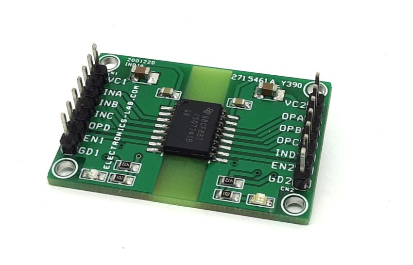
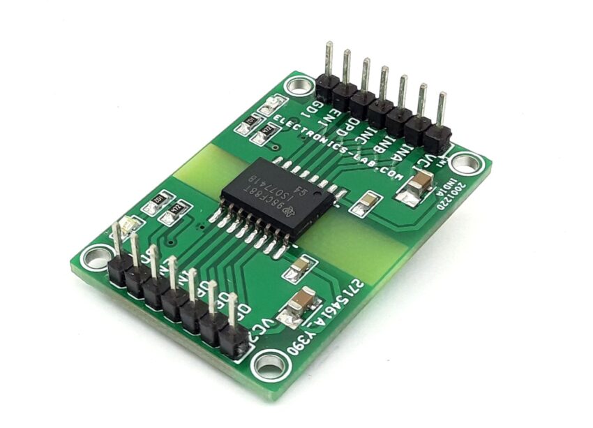
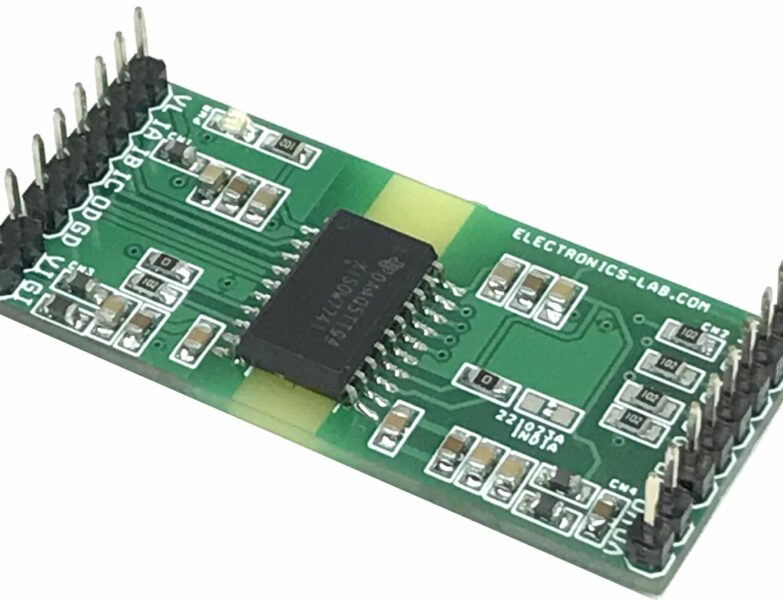
The project described here is a Quad-channel digital isolator with 5000VRMS isolation ratings per UL 1577. The board has three forward and one reverse-direction channel which makes this project ideal for isolated SPI interface between microcontroller and subnode unit. The circuit provides isolation between the main SPI unit (microcontroller) and the SPI slave. It has high electromagnetic immunity, reduces noise, and high voltage traveling to the main unit. All the outputs are normally high, use ENABLE pins to disable the outputs. Connecting Enable 1 and Enable 2 pins to GND respective sides puts all outputs LOW and all outputs are disabled. If the input power or signal is lost then the output goes high. Level translation range: 2.25V to 5.5V.
4-wire SPI devices have four signals, 3 Forward and One Reverse-Direction
- Clock (SPI CLK, SCLK)
- Chip select (CS)
- main out, subnode in (MOSI)
- main in, subnode out (MISO)
More info about SPI: https://www.analog.com/en/analog-dialogue/articles/introduction-to-spi-interface.html
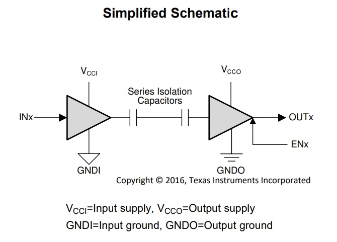
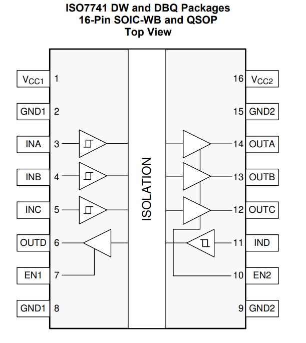
The ISO7741 device is a high-performance, quad-channel digital isolator with 5000 VRMS isolation ratings per UL 1577. This family includes devices with reinforced insulation ratings according to VDE, CSA, TUV, and CQC. The ISO7741B device is designed for applications that require basic insulation ratings only. The ISO7741 device provides high electromagnetic immunity and low emissions at low power consumption while isolating CMOS or LVCMOS digital I/Os. Each isolation channel has a logic input and output buffer separated by a double capacitive silicon dioxide (SiO2) insulation barrier. These devices come with enable pins which can be used to put the respective outputs in high impedance for multi-master driving applications and to reduce power consumption. The ISO7741 device has three forward and one reverse-direction channel.
Features
- Wide supply range: 2.25 V to 5.5 V Main SPI Side
- Wide supply range: 2.25 V to 5.5 V Subnode SPI Side
- Level Translation Range: 2.25V to 5.5V
- 2 x Power LED Main SPI side and Subnode Side
- 100 Mbps data rate
- Robust isolation barrier
- 100-year projected lifetime at 1500 VRMS working voltage
- Up to 5000 VRMS isolation rating
- Up to 12.8 kV surge capability
- ±100 kV/µs typical CMTI
- Default output high
- Wide temperature range: –55°C to 125°C
- Low power consumption, typical 1.5 mA per channel at 1 Mbps
- Low propagation delay: 10.7 ns typical (5-V Supplies)
- Robust electromagnetic compatibility (EMC)
- System-level ESD, EFT, and surge immunity
- ±8 kV IEC 61000-4-2 contact discharge protection across the isolation barrier
- Low emissions
- PCB dimensions: 40.64 x 27.94mm
Schematic
Simplified Schematic
IC Pinout and Internal Diagram
Parts List
| NO | QNTY | REF | DESC. | MANUFACTURING | SUPPLIER | PART NO |
|---|---|---|---|---|---|---|
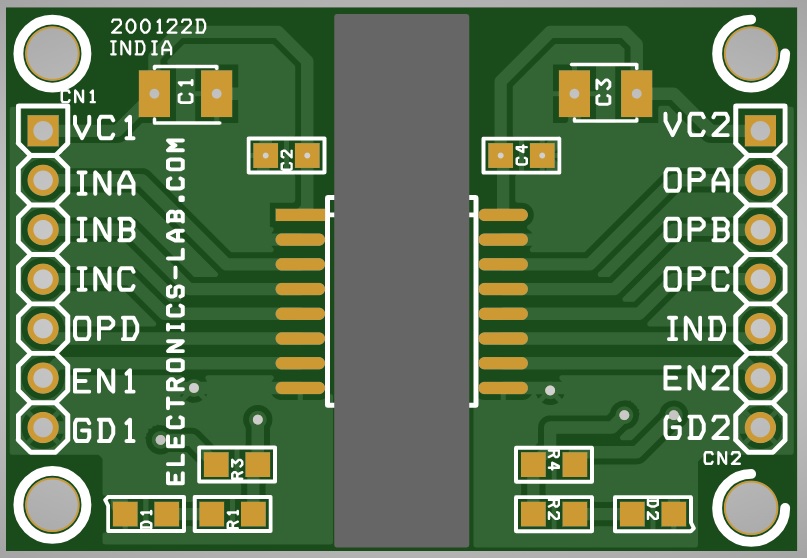
| 1 | 2 | CN1,CN2 | 7 PIN MALE HEADER PITCH 2.54MM | WURTH | DIGIKEY | 732-5320-ND |
| 2 | 2 | C1,C3 | 10uF/10V SMD SIZE 1210 OR 1206 | YAGEO/MUARATA | DIGIKEY | |
| 3 | 2 | C2,C4 | 0.1uF/50V SMD SIZE 0805 | YAGEO/MUARATA | DIGIKEY | |
| 4 | 2 | D1,D2 | LED RED OR GREEN SMD SIZE 0805 | LITE ON INC | DIGIKEY | 160-1427-1-ND |
| 5 | 2 | R1,R2 | 1K 5% SMD SIZE 0805 | YAGEO/MUARATA | DIGIKEY | |
| 6 | 1 | R3 | 4K7 5% SMD SIZE 0805 | YAGEO/MUARATA | DIGIKEY | |
| 7 | 1 | U1 | ISO7741DWR | TI | DIGIKEY | 296-47781-1-ND |
Connections


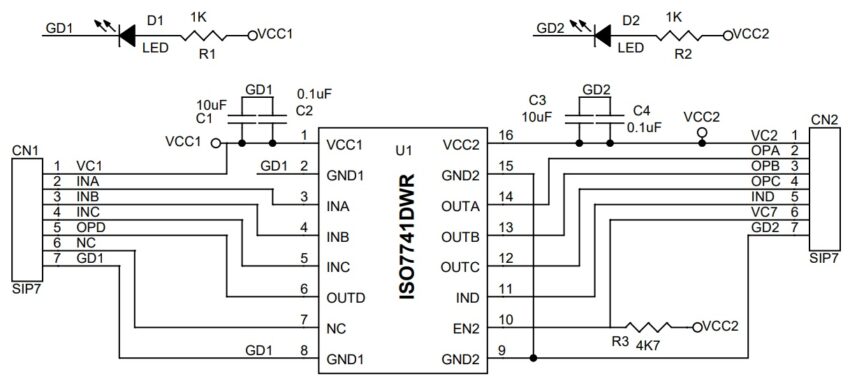
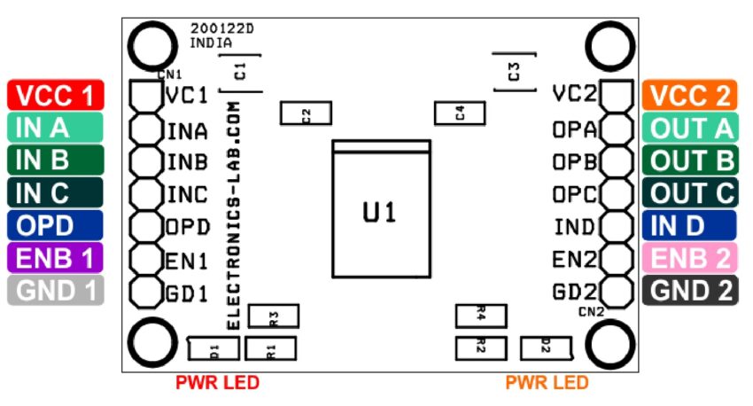

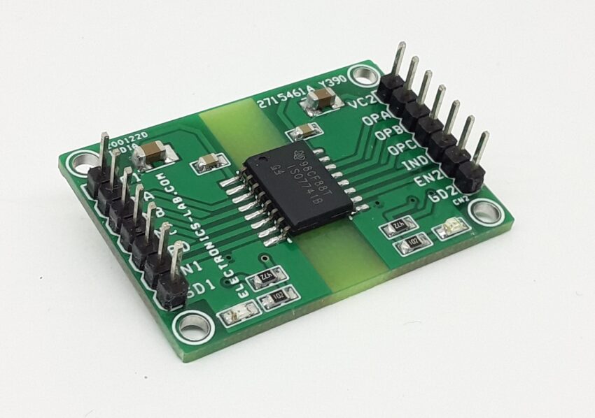
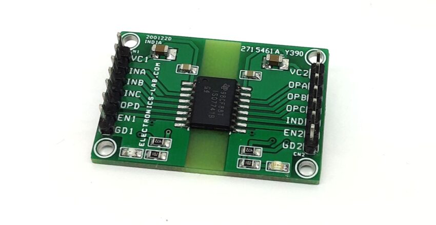
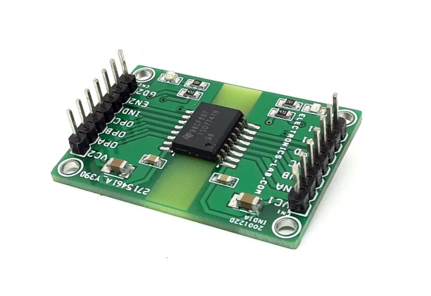
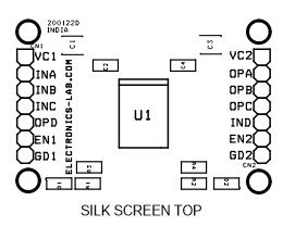
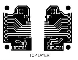
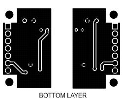


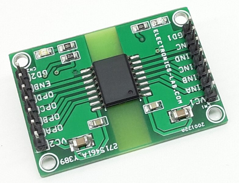
The current schematics is outdated. Please check R3, R4 and the missing EN1 in the schematics