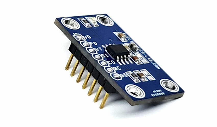
AMR Angle Sensor and Signal Conditioner Module
- Rajkumar Sharma
- 39 Views
- easy
- Tested
- SKU: EL153660
- Quote Now
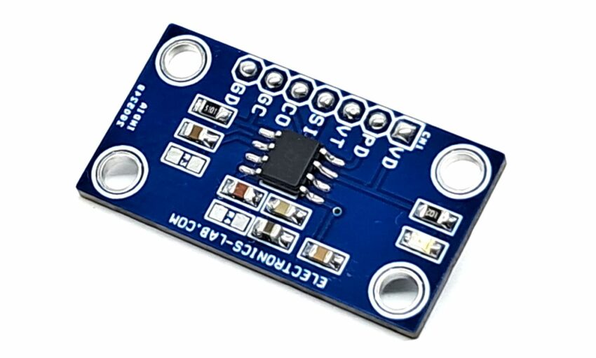
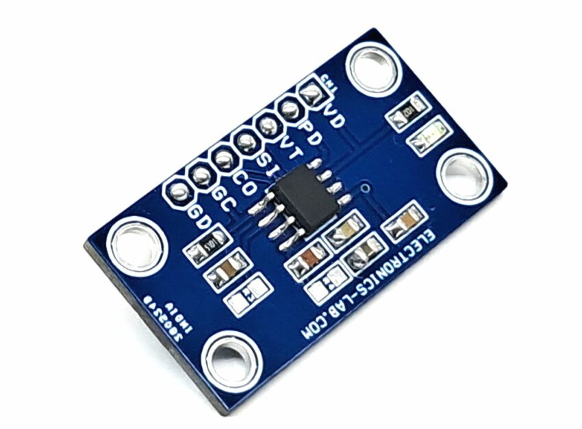
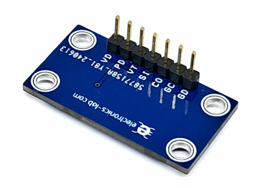
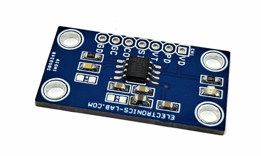
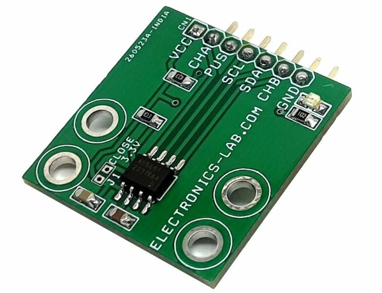
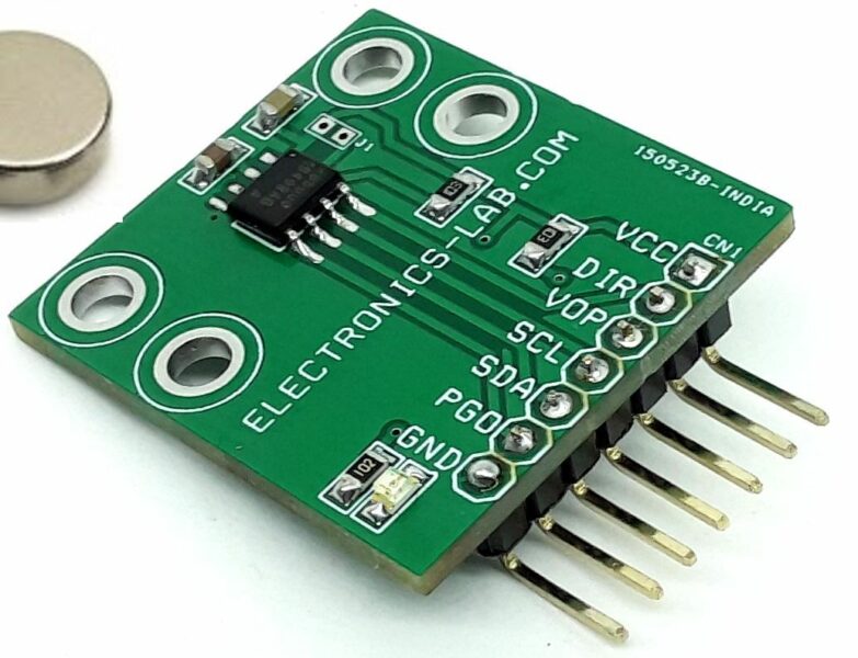
This angle sensor module features an ADA4571 chip, an anisotropic magneto resistive (AMR) sensor with integrated signal conditioning amplifiers and ADC drivers. The circuit produces two analog outputs that indicate the angular position of the surrounding magnetic field.
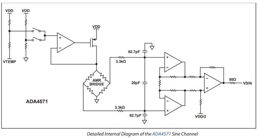
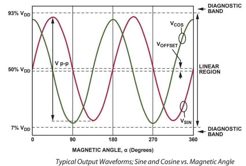
The ADA4571 consists of two die within one package, an AMR sensor, and a fixed gain (G = 40 nominally) instrumentation amplifier. The ADA4571 delivers clean and amplified cosine and sine output signals related to the angle of a rotating magnetic field. The output voltage range is Ratiometric to the supply voltage. The sensor contains two Wheatstone bridges, at a relative angle of 45° to one another. A rotating magnetic field in the x-y sensor plane delivers two sinusoidal output signals with the double frequency of the angle (α) between the sensor and magnetic field direction. Within a homogeneous field in the x-y plane, the output signals are independent of the physical placement in the z direction (air gap).
Features
- Power Supply 2.7V to 5.5V DC
- Quiescent Supply Current 7mA (Only Chip), No LED
- High precision 180° angle sensor
- Maximum angular error of 0.5°
- Analog sine and cosine outputs
- Power Up Time 150uS
- Ratiometric output voltages
- Low thermal and lifetime drift
- Temperature Voltage Range -40 to 150 Degree Centigrade (0 to 80% of VDD)
- SAR or Σ-∆ analog-to-digital converter (ADC) drive capable
- Magnetoresistive (MR) bridge temperature compensation mode
- Contactless angular measurement.
- Measures magnetic field direction rather than field intensity.
- Minimum sensitivity to air gap variations.
- Large working distance.
- Excellent accuracy, even for weak saturation fields.
- Negligible hysteresis.
- Temperature range: −40°C to +150°C
- EMI resistant
- Fault diagnostics
- Minimum phase delay
- PCB Dimensions 33.18 X 17.78MM
- 4 X 2.5MM Mounting Holes
ADA4571 – Integrated AMR Angle Sensor and Signal Conditioner
Reference Position Error
The reference position error is the absolute mounting position deviation of the sensor from its nominal placement. The reference position for Y = 0 µm is the straight connection line of Pin 2 and Pin 7. The X = 0 µm position is referred to the middle distance of the package top. The position accuracies are within a precision of ±0.05 mm (±50 µm) in both the X and Y direction.
Reference Angle Error
The reference angle error is the absolute mounting rotation deviation of the sensor from its nominal placement. Marking the position for angle Φ= 0° position is referred parallel to the straight connection line of Pin 2 and Pin 7.
VTEMP Output Pin (CN1 Pin 3)
A proportional to absolute temperature circuit provides a voltage output at the VTEMP pin for temperature monitoring or temperature calibration purposes. The output voltage is ratiometric to the supply voltage enabling the interface with an ADC that uses the supply voltage to generate the reference voltage. This pin must be left open when not in use.
Power-Down Mode (CN1 Pin 2)
Power-down mode can be activated by switching the PD pin to the VDD pin. Within this mode, the device shuts down and its output pins are set to high impedance to avoid current consumption across the load resistors. The VTEMP output is connected to ground through a pull-down resistor. Power-down mode can be entered with GC = VDD or GC = GND. An internal pull-down resistor ensures that the device remains active if the PD pin is left floating.
Gain Control Mode (CN1 Pin 6)
Gain control (GC) enable mode can be activated by switching the GC pin to the VDD pin. In this mode, the AMR bridge sensor amplitude outputs are compensated to reduce temperature variation. This results in higher and controlled output voltage levels, boosting system dynamic range and easing the system design task. If the GC pin is left floating, a weak pull-up resistor ensures that the GC mode is enabled as a default condition. The GC mode can also be used as a sensor self-diagnostic by comparing the sine and cosine amplitude outputs when enabled and disabled, such as radius check. In the event that the radius does not change, it indicates a gross failure in the IC.
Power Consumption
Worst case quiescent power occurs when the supply current runs at its specified maximum of 7 mA and the ADA4571 is run at the maximum VDD of 5.5 V, giving a worst-case quiescent power of 38.5 mW. The power consumption is dependent on VDD, temperature, load resistance (RL), load capacitance (CL), and frequency of the rotating magnetic field. It is recommended to refer RL and CL to ground. The output voltages are protected against short circuit to the VDD pin or ground by current limitation within the given time duration. Placing the device 180° rotated into the socket may lead to damages if the supply current is not limited to 100 mA.
Offset of Signal Outputs
The single-ended output signals are referenced to VDD/2 generated internally on-chip. Offsets originate from matching inaccuracies and other imperfections during the production process. For tight tolerances, it is required to match the external loads for VSIN and VCOS to each other. For ESD and EMC protection, the outputs contain a series resistance of 50 Ω. The influence of this series resistance is minimized with a large output load resistance.
Signal Dependence on Air Gap Distance
The IC measures the direction of the external magnetic field within its x-y plane. The result is widely independent of the field strength as long as it is above the specified minimum value of 25 kA/m. Within a homogeneous field in x-y direction, the result is independent of its placement in z direction (air gap). The nominal z distance of the internal x-y plane to the top surface of the plastic package is 0.400 mm.
Connections
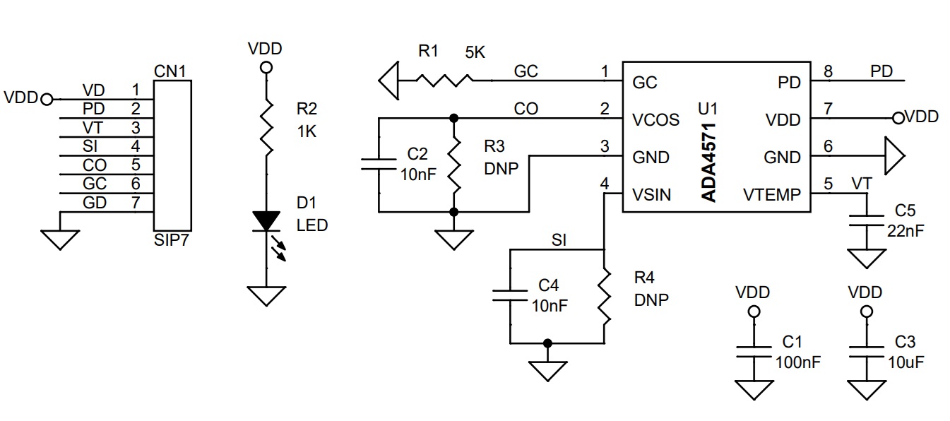
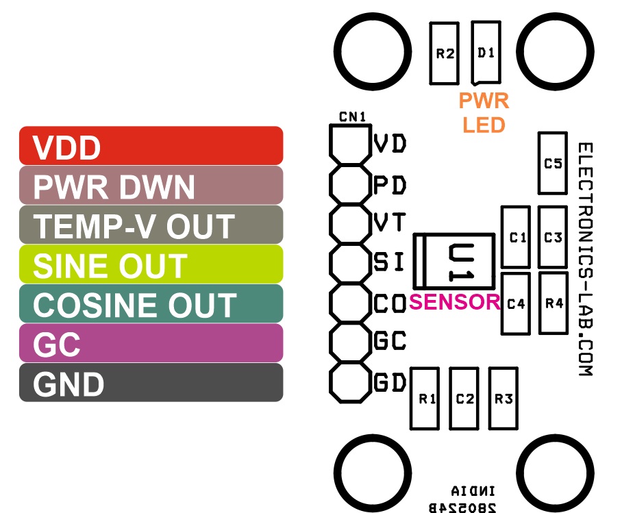
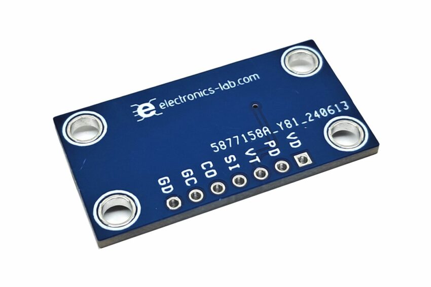
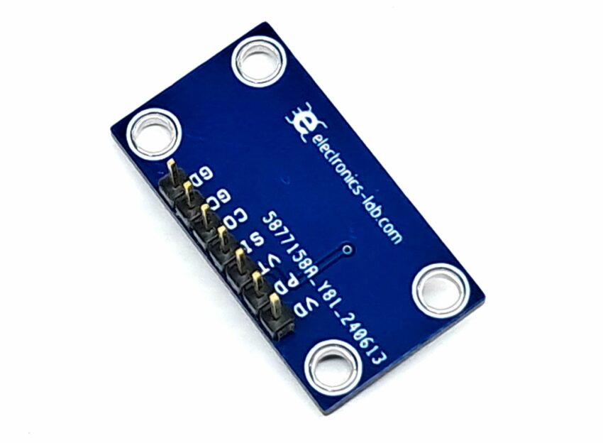
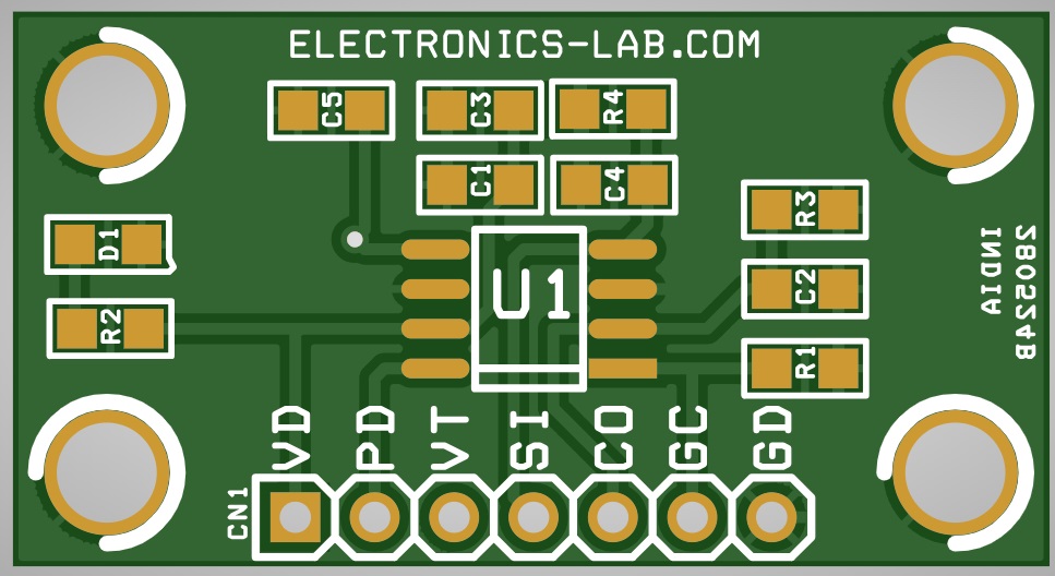
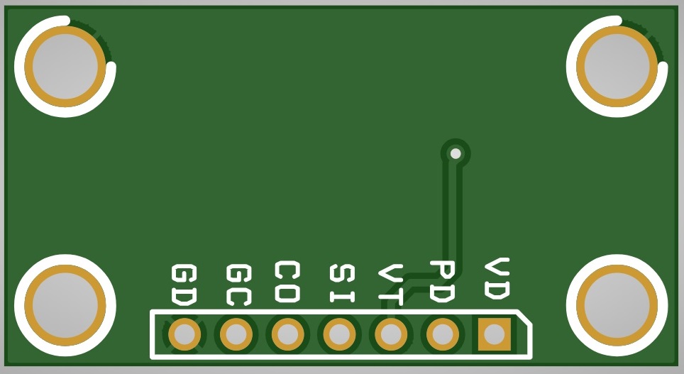
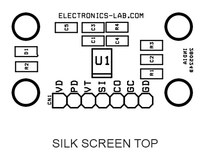
- CN1: Pin 1 = VDD 2.7V-5.5V DC, Pin 2 = Power Down (PD) Active High, Pin 3 = Voltage Temperature Output (VT), Pin 4 = Analog Sine Output, Pin 5 = Analog Cosine Output, Pin 6 = Gain Control Mode Enable (GC), Pin 7 GD
- D1: Power LED
Schematic
Parts List
| NO. | QNTY. | REF. | DESC. | MANUFACTURER | SUPPLIER | SUPPLIER PART NO |
|---|---|---|---|---|---|---|
| 1 | 1 | CN1 | 7 PIN MALE HEADER PITCH 2.54MM | WURTH | DIGIKEY | 732-5320-ND |
| 2 | 1 | C1 | 100nF/10V CERAMIC SMD SIZE 0805 | YAGEO/MURATA | DIGIKEY | |
| 3 | 2 | C2,C4 | 10nF/10V CERAMIC SMD SIZE 0805 | YAGEO/MURATA | DIGIKEY | |
| 4 | 1 | C3 | 10uF/10V CERAMIC SMD SIZE 0805 | YAGEO/MURATA | DIGIKEY | |
| 5 | 1 | C5 | 22nF/10V CERAMIC SMD SIZE 0805 | YAGEO/MURATA | DIGIKEY | |
| 6 | 1 | D1 | LED RED SMD SIZE 0805 | OSRAM | DIGIKEY | 475-1278-1-ND |
| 7 | 1 | R1 | 5K 1% SMD SIZE 0805 | YAGEO/MURATA | DIGIKEY | |
| 8 | 1 | R2 | 1K 5% SMD SIZE 0805 | YAGEO/MURATA | DIGIKEY | |
| 9 | 2 | R3,R4 | DNP | DO NOT USE | ||
| 10 | 1 | U1 | ADA4571 SOIC8 | ANALOG DEVICE | DIGIKEY | 505-ADA4571BRZ-ND |
ADA4571 Block Diagram
Output Signal Angle vs Amplitude
Connections


