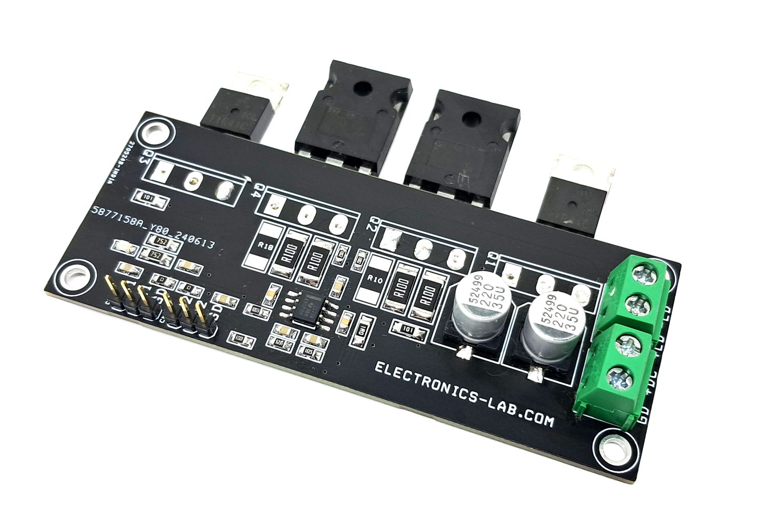
Dual Channel Voltage-to-Current (V-I) converter circuit with BJT
- Rajkumar Sharma
- 40 Views
- medium
- Tested
- SKU: EL154054
- Quote Now
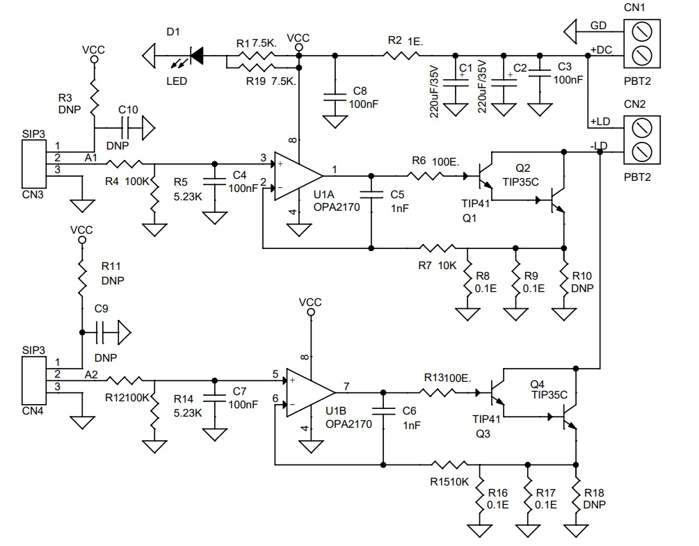
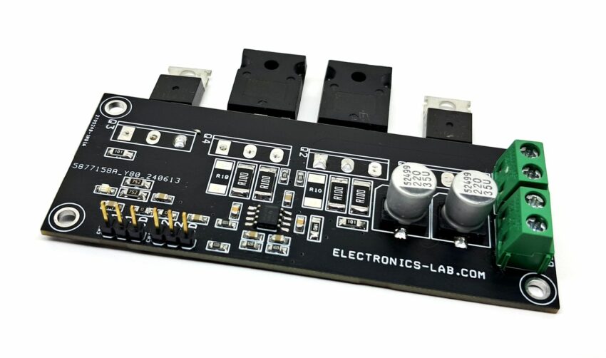
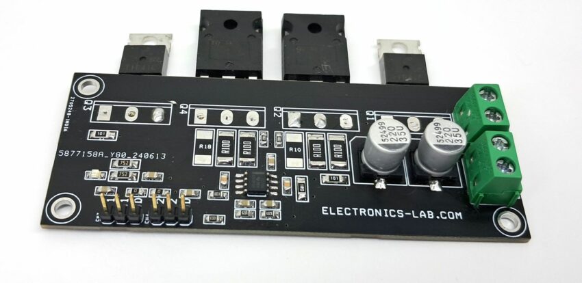
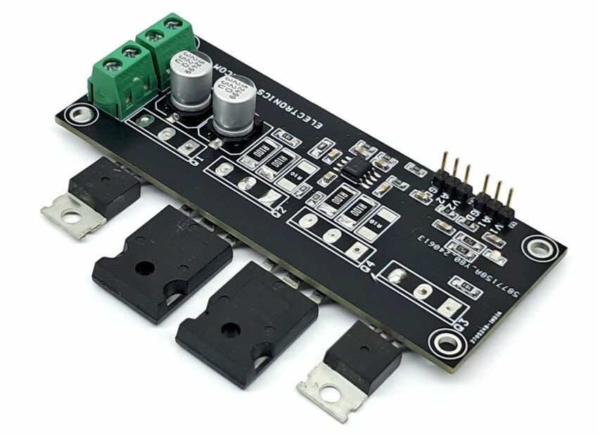
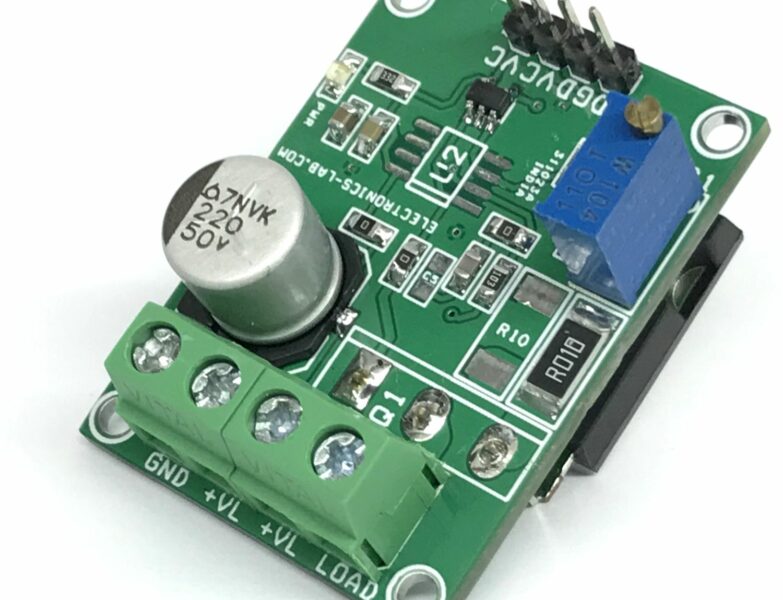
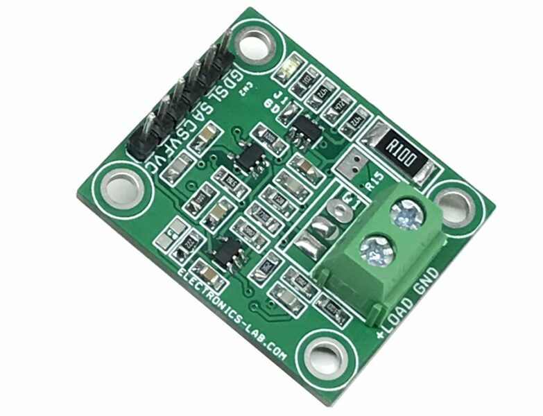
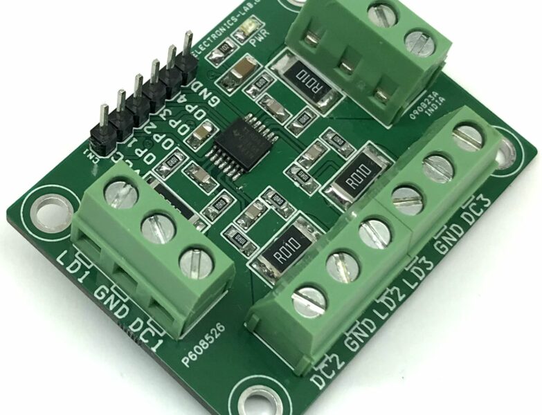
This low-side voltage-to-current (V-I) converter delivers a well-regulated current to a load. The circuit accepts an input voltage from 0V to 3V and converts it to a current from 0A to 6A (combined). The current is accurately regulated by feeding back the voltage drop across a low-side current-sense resistor (R8, R9 + R16, R17) to the OPAMP. Resistor divider (R4 and R5 + R12 and R13) is implemented to limit the maximum voltage at the non-inverting input, Vin, and sense resistor, (R8, R9 + R16, R17), at full-scale. Using a Darlington BJT reduces the output current requirement for the OPAMP. Feedback components R6+R13, R7+R15, and C5+C6 provide compensation to ensure stability. R6+R13 isolates the input capacitance of the bipolar junction transistor (BJT) R7+R15 provides a DC feedback path directly at the current setting resistor (R8, R9 + R16, R17), and C5+C6 provides a high-frequency feedback path that bypass the BJT.
The project is built using the OPA2170 dual OPAMP, which enables the creation of two separate channels. Each channel is capable of handling a current of up to 3A, and when combined, they provide a total current of 6A. Users have the flexibility to utilize only one channel if a lower current is required, in which case the components associated with the second channel can be omitted. To achieve a 6A load, simply tie inputs A1 and A2 together. For a 3A load, only one input is necessary.
Features
- Input Power Supply Range 12V to 30V DC
- Load 5Amps (3A + 3A)
- Input Voltage 0 to 3V
- 4 x 4 mm Mounting Holes
- On Board Power LED
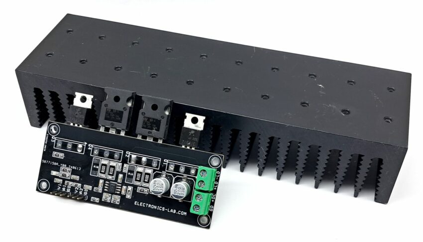
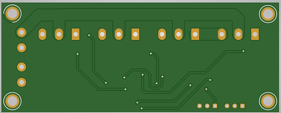
- PCB Dimensions 91.44 x 36.20 mm
Connections
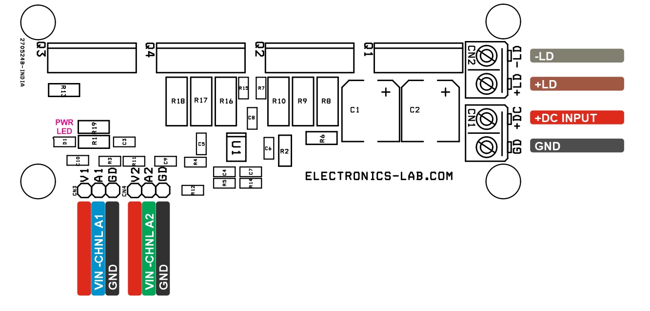
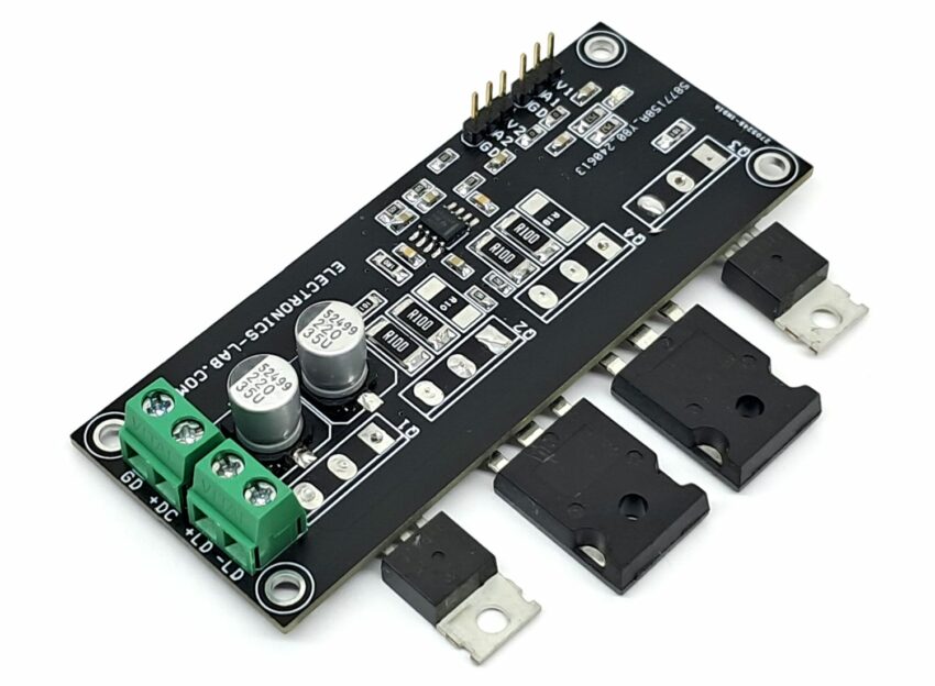
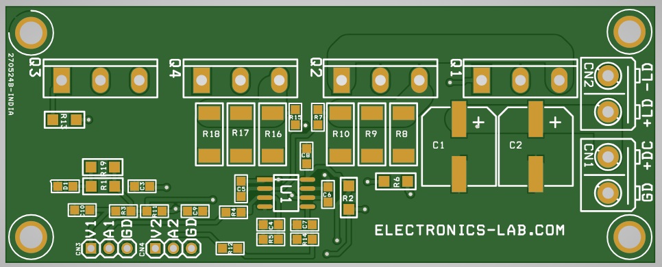
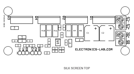
- CN1: Pin 1 = Power Supply Input 12V TO 30V, Pin 2 = GND
- CN2: Pin 1 = +Load, Pin 2 = -Load
- CN3: Pin 1 = No Use, Pin 2 = Analog Voltage in for Channel A1, Pin 3 = GND
- CN4: Pin 1 = No Use, Pin 2 = Analog Voltage in for Channel A2, Pin 3 = GND
- D1: Power LED
Schematic
Parts List
| NO. | QNTY. | REF. | DESC. | MANUFACTURER | SUPPLIER | SUPPLIER PART NO |
|---|---|---|---|---|---|---|
| 1 | 2 | CN1,CN2 | 2 PIN SCREW TERMINAL PITCH 5.08MM | PHOENIX | DIGIKEY | 277-1247-ND |
| 2 | 2 | CN3,CN4 | 3 PIN MALE HEADER PITCH 2.54MM | WURTH | DIGIKEY | 732-5316-ND |
| 3 | 2 | C1,C2 | 220uF/35V | RUBYCON | DIGIKEY | 1189-35SGV220M10X10.5CT-ND |
| 4 | 4 | C3,C4,C7,C8 | 100nF/50V CERAMIC SMD SIZE 0805 | YAGEO/MURATA | DIGIKEY | |
| 5 | 2 | C5,C6 | 1nF/50V CERAMIC SMD SIZE 0805 | YAGEO/MURATA | DIGIKEY | |
| 6 | 6 | R3,C9,R10,C10,R11,R18 | DNP | |||
| 7 | 1 | D1 | LED RED SMD SIZE 0805 | LITE ON INC | DIGIKEY | 160-1427-1-ND |
| 8 | 2 | Q1,Q3 | TIP41 TO220 | ST | DIGIKEY | 497-2622-5-ND |
| 9 | 2 | Q2,Q4 | TIP35C TO247 | ST | DIGIKEY | 497-2609-5-ND |
| 10 | 2 | R1,R19 | 7.5K 5% SMD SIZE 1206 | YAGEO/MURATA | DIGIKEY | |
| 11 | 1 | R2 | 1E 5% SMD SIZE 1206 | YAGEO/MURATA | DIGIKEY | |
| 12 | 2 | R4,R12 | 100K 1% SMD SIZE 0805 | YAGEO/MURATA | DIGIKEY | |
| 13 | 2 | R5,R14 | 5.23K 1% SMD SIZE 0805 | YAGEO/MURATA | DIGIKEY | |
| 14 | 2 | R6,R13 | 100E 5% SMD SIZE 1206 | YAGEO/MURATA | DIGIKEY | |
| 15 | 2 | R7,R15 | 10K 5% SMD SIZE 0805 | YAGEO/MURATA | DIGIKEY | |
| 16 | 4 | R8,R9,R16,R17 | 0.1E 1% 3W SMD SIZE 2512 | BOURNS | DIGIKEY | CRA2512-FZ-R100ELFCT-ND |
Connections


