Half-Bridge with Over Current Protection – 400V/1A
- Rajkumar Sharma
- 12 Views
- moderate
- Tested
- SKU: EL156782
- Quote Now
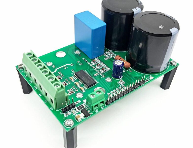
The Half-Bridge Driver project presented here is designed to support load power supplies of up to 400V DC. The board features the IRS2890DS Half-Bridge Gate Driver IC, which is paired with two IGBTs rated at 8A/650V, conveniently mounted on the board. The board features overcurrent shutdown. Barrier Terminal Blocks provided for load and input supply.
Features
- Load Power Supply 400V DC
- Maximum Load 1Amps
- Logic Gate Driver Power Supply 15V-16V DC (VC/VCC)
- Fault Clear/Enable Power Supply 3.3V-5V (VD)
- Fault Clear Time Approx. 1mS
- Over Current Protection Threshold 4.58A (I-TRIP)
- Short Circuit Time Constant 1-2uS
- HIN/LIN Input Signal ,3.3 V, 5 V, and 15 V Logic-compatible
- Overcurrent Protection, Fault Reporting and Enable
- Barrier Terminal Blocks for Power and Load
- Header Connector for Gate Driver Supply, Inputs, RFE and VD 3.3-5V
- 4 x 4 mm PCB Mounting Holes
- PCB Dimensions 60.01 x 34.93 mm
Functions
- Overcurrent shutdown
- Undervoltage lockout for both high-side and low-side
- Cross-conduction prevention
- All switches turn off during protection
- Active-high input signal logic
Load Handling and Overcurrent Protection
The board is capable of handling loads of up to 1Amp, making it suitable for a variety of applications. The overcurrent trip point is set to 4.58A, providing an added layer of protection against overcurrent conditions. In the event of a fault, the board is designed to clear the condition within 1ms, minimizing downtime and ensuring rapid recovery.
Configuring the Board for Custom MOSFET/IGBT Applications
The board can be tailored to meet specific user requirements for switching frequency, DC bus voltage and current. The gate driver chip is designed to drive either IGBT or MOSFET, with provisions for using TO263/D2PK MOSFET/IGBT components. To ensure optimal performance, it is crucial to select a MOSFET/IGBT that matches the output current capacity of the chip, which has a current sink/source capacity of 220mA/480mA. Key Considerations for Configuring the Board with an Alternative MOSFET/IGBT, following factors must be taken into account: Bootstrap Capacitor Value: This value is dependent on the operating frequency and should be selected accordingly. Gate Resistors and Diodes (R2, R3, R4, R6, D1, D2): D1 and D2 are 1N4148-type diodes, and all resistors are 0805 size. These components should be chosen based on the specific requirements of the MOSFET/IGBT being used. DC Bus Capacitors (C3, C4): The value and voltage of these capacitors must be carefully selected to ensure reliable operation. Shunt Resistor Value for Over Current Protection: This value is critical for protecting the board from overcurrent conditions and should be chosen based on the specific requirements of the application. Time Constant (R7 and C8): The default time constant is set to 1-2μs for overcurrent shutdown. This value can be adjusted as needed to suit the specific application. Fault Clear Time (R5 and C7): This value determines the time it takes for the board to clear a fault condition and should be chosen based on the specific requirements of the application.
Over Current Protection
The integrated comparator is triggered, if the voltage VITRIP is higher than 0.5 V. In case of a trigger event, the voltage at pin RFE is pulled down to low. The IRS2890DS has an overcurrent shutdown function. Its internal comparator monitors the voltage of the ITRIP pin, and if this voltage exceeds the VITRIP+, which is specified in the device’s datasheets, a fault signal is activated and all channels are turned off. Typically, the maximum short-circuit current magnitude is gate voltage dependant. A higher gate voltage results in a larger short-circuit current.
Fault output, Fault clear timer and Enable pin
This is the fault output alarm pin. An active low output is given on this pin for a fault-state condition in the IRS2890DS. The alarm conditions are overcurrent detection and low-side bias UV (undervoltage) operation. The RFE output is open-drain configured. The RFE signal line is pulled up to the logic power supply (5 V or 3.3 V) with resistance R5 and capacitor C7 between RFE and COM pins to program fault clear time. Externally pulling down the pin can disable the output; for normal operation, this pin default pulled up.
Fault output circuit and fault-clear time setup
The IRS2890DS provides adjustable fault-clear timer. Once ITRIP pin recognizes a fault, the RFE pin is internally pulled to COM. The RFE output stays in the low state until the fault condition has been removed and the fault clear timer expires; once the fault-clear timer expires, the voltage on the RFE pin will return to its external pull up voltage. The length of the fault-clear time period (TFLTCLR) is determined by the exponential charging characteristics of the capacitor, where the time constant is set by R5 and C7. The length of the fault-clear time period is approx. 1mS. User may refer data sheet of the chip for more information to change the fault clear time.
Enable input circuit
IRS2890DS provides an enable functionality that allows it to shut down or enable the output. When the RFE pin is externally pulled up, the HVIC is able to operate normally (assuming no other fault conditions: undervoltage protection of VCC or overcurrent protection of ITRIP). When the RFE pin is pulled down externally, the gate drive outputs are pulled low until the enable condition is restored.
Input Signal
The input signals are active-high configured. There is an internal pull-down resistor from each input signal line to COM.
Operating Frequency & Test
Test is conducted with 6.5Khz input frequency, board can support frequency up to 20Khz. Resistor used as load to conduct the test.
Undervoltage protection
This IC provides undervoltage lockout protection on both the VCC (logic and low-side circuitry) power supply and the VBS (high-side circuitry) power supply.
High Voltage Warning
It is important to note that the project operates with lethal voltage, and users must take all necessary safety precautions before testing the board. After the power is off, the DC bus capacitors remain charged and have lethal voltage, requiring an appropriate waiting time for capacitor discharge before conducting tests.
Gate Driver Chip Features
- Floating channel designed for bootstrap operation
- Fully operational to +600 V
- Tolerant to negative transient voltage, dV/dt immune
- Gate drive supply range from 10 V to 20 V
- Undervoltage lockout for both channels
- 3 V, 5 V, and 15 V input logic-compatible
- Matched propagation delay for both channels
- Lower di/dt gate driver for better noise immunity
- Outputs in phase with inputs
- Integrated bootstrap FET
- Suitable for both trapezoidal and sinusoidal motor control
- Overcurrent protection, fault reporting and enable
Connections
- CN1 Power Input: Pin1 = Load Power Supply 400V DC, Pin 2 = GND
- CN2: Pin 1 = VCC 12V-15V DC, Pin 2 High Input, Pin 3 = Low Input, Pin 4 = RE/Fault, Pin 5 = GND, Pin 6 = 3.3V-5V DC
- CN3 Load: Pin 1 = GND, Pin2 = Output
- D3: Power LED
Schematic
Parts List
| NO | QNTY. | REF | DESC | MANUFACTURER | SUPPLIER | SUPPLIER PART NO |
|---|---|---|---|---|---|---|
| 1 | 2 | CN1,CN3 | 2 PIN SCREW TERMINAL PITCH 5.08MM | PHOENIX | DIGIKEY | 277-1247-ND |
| 2 | 1 | CN2 | 6 PIN MALE HEADER PITCH 2.54MM | WURTH | DIGIKEY | 732-5319-ND |
| 3 | 2 | C1,C6 | 100nF/50V CERAMIC SMD SIZE 0805 | YAGEO/MURATA | DIGIKEY | |
| 4 | 1 | C2 | 220uF/25V ELECTROLYTIC 8MM-DIA | WURTH | DIGIKEY | 732-8829-1-ND |
| 5 | 1 | C3 | 0.47uF/275VX2 | WURTH | DIGIKEY | 732-5805-ND |
| 6 | 1 | C4 | 15uF/450V ELECTROLYTIC 12.5MM-DIA | RUBYCON | DIGIKEY | 1189-3177-ND |
| 7 | 1 | C5 | 0.47uF/35V CERAMIC SMD SIZE 1206 | YAGEO/MURATA | DIGIKEY | |
| 8 | 2 | C7,C8 | 1nF/50V CERAMIC SMD SIZE 0805 | YAGEO/MURATA | DIGIKEY | |
| 9 | 6 | D1,R2,D2,R4,R9,R11 | DNP | |||
| 10 | 1 | D3 | LED RED SMD SIZE 0805 | OSRAM | DIGIKEY | 475-1278-1-ND |
| 11 | 2 | Q1,Q2 | RGT8NS650 D2PAK TO263 | ROHM | DIGIKEY | RGT8NS65DGTLCT-ND |
| 12 | 3 | R1,R3,R6 | 10E 5% SMD SIZE 0805 | YAGEO/MURATA | DIGIKEY | |
| 13 | 1 | R5 | 1M 5% SMD SIZE 0805 | YAGEO/MURATA | DIGIKEY | |
| 14 | 1 | R7 | 1.8K 5% SMD SIZE 0805 | YAGEO/MURATA | DIGIKEY | |
| 15 | 1 | R8 | 2.2K 5% SMD SIZE 0805 | YAGEO/MURATA | DIGIKEY | |
| 16 | 1 | R10 | 0.12E/3W 1% SMD SIZE 2512 | TE CONNECTIVITY | DIGIKEY | 1712-TLRP3A30WR120FTECT-ND |
| 17 | 1 | U1 | IRS2890 SOIC14 | INFINEON | DIGIKEY | IRS2890DSTRPBFCT-ND |
Connections
Block Diagram
Typical Application


