

High-Voltage (180V) – High-Current (30mA) Operational Amplifier Module
- Rajkumar Sharma
- 162 Views
- moderate
- Tested
- SKU: EL148358
- Quote Now
- 0 Likes

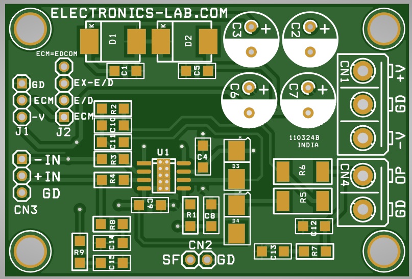
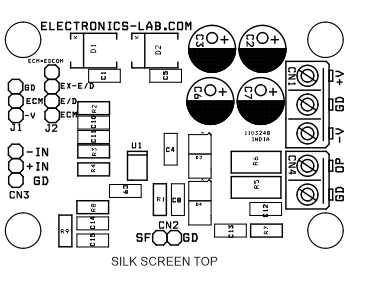
This project provides a platform to evaluate the OPA462 high-voltage, high-current operational amplifier. Multiple component footprints allow the most common circuit configurations. The board accommodates high-voltage and high-current operational amplifier OPA462 from Texas Instruments. A High-Voltage Noninverting Amplifier, AV = 17 V/V. An example application circuit is given below. The board is capable of operating with supply voltages as high as ±90 V (180 V), or as low as ±6 V (12 V). The high-voltage process and design of the OPA462 allow the device to be used in applications where most operational amplifiers cannot be applied, such as high-voltage power-supply conditions, or when there is a need for a very high-output voltage swing. The output is capable of delivering up to ±30 mA output current or swinging within a few volts of the supply rails at moderate current levels. The OPA462 features input overvoltage protection, output current limiting, thermal protection, a status flag, and enable-disable capability. The output swing is 85V with 5V AC signal input and frequency 10Khz. Status Flag is an open-drain active-low output referenced to E/D Com. This pin goes active for either an overcurrent or overtemperature condition. Close (Link) Shunt between GD and E/D Com to enable the output, and Close E/D and E/D Com Jumper J2 to disable the Output.
For Normal operation connect Jumper/Shunt between GD and E/D Com, Jumper J2 open. Use 0 ohms resistors of 1206 Size instead of capacitors C14 and C15. Many optional components are provided for different applications, all capacitors and resistors are SMD 1206. R5 and R6 resistors are SMD 2512 size.
Features
- Wide power-supply range:
- ±90 V (180 V) (Supply Range ±6 V (12 V) to ±90 V (180 V)
- High-output load drive: IO ±45 mA
- Output Voltage 85V
- Input Signal 5V AC
- Gain 17V/V
- Flexible design allows a wide variety of circuit configurations
- Includes protection against power supply sequencing and inductive load kickback
- Current limit protection
- Thermal protection
- Status flag Output
- Independent output disables
- Gain bandwidth: 6.5 MHz
- Slew rate: 32 V/µs
- 4 x 4 mm PCB Mounting Holes
- Screw Terminals for Power Input and Output
- Header Connector for Signal Input
- Jumper J1 and J2 for Enable/Disable
- PCB Dimensions 60.96 x 41.28 mm
A noninverting circuit with a moderately high closed-loop gain (AV) of 17 V/V (24.6 dB). In this example, a 5-VPK ac signal is amplified to 85 VPK across a 10-kΩ load resistor connected to the output. The peak current for this application is 8.5 mA, and is well within the OPA462 output current capability. Higher output current, typically up to 30 mA, may be attained at the expense of the output swing to the supply rails. A ±90-VDC power supply is required for this configuration. The noninverting amplifier circuit shows the OPA462 enable-disable function. When placed in disabled mode the op amp becomes non-functional, and the current consumption is reduced to approximately one-third to one-half the enabled level. An enable active state occurs when the E/D pin is left open, or is biased 3 V to 5 V greater than the E/D Com voltage level. If biased between the E/D com level, to E/D Com + 0.65 V, the OPA462 disables. Diode provided at output to protect against back electromagnetic force (EMF).
A potentially destructive mechanism is the back EMF transient that can be generated when driving an inductive load. D3, D4, D1 and D2 in circuit have been added to the basic OPA462 amplifier circuit to provide protection in the event of back EMF. If the voltage at the OPA462 output attempts to momentarily rise above V+, D3 becomes forward-biased and clamps the voltage between the output and V+ pins. This clamp must be sufficient to protect the OPA462 output transistor. If the event causes the V+ voltage to increase the power supply bypass capacitor, D1, or both, a Zener diode or a transient voltage suppressor (TVS) can provide a path for the transient current to ground. D4 and D2 provide the same protection in the negative supply circuit.
The OPA462 noninverting amplifier circuit with a closed-loop gain of 17 V/V has a small-signal, –3-dB bandwidth of nearly 800 kHz. However, the large-signal bandwidth is likely of greater importance in a high-output-voltage application. For that mode of operation, the slew rate of the op amp and the peak output swing voltage must be considered in order to determine the maximum large-signal bandwidth. The slew rate (SR) of the OPA462 is typically 6.5 V/µs, or 6.5 × 10⁶ V/s.
The best practice for a typical parameter such as slew rate to allow for variance. In this example, keeping the large signal fMAX to 10 kHz is sufficient to make sure the output avoids slew rate limiting
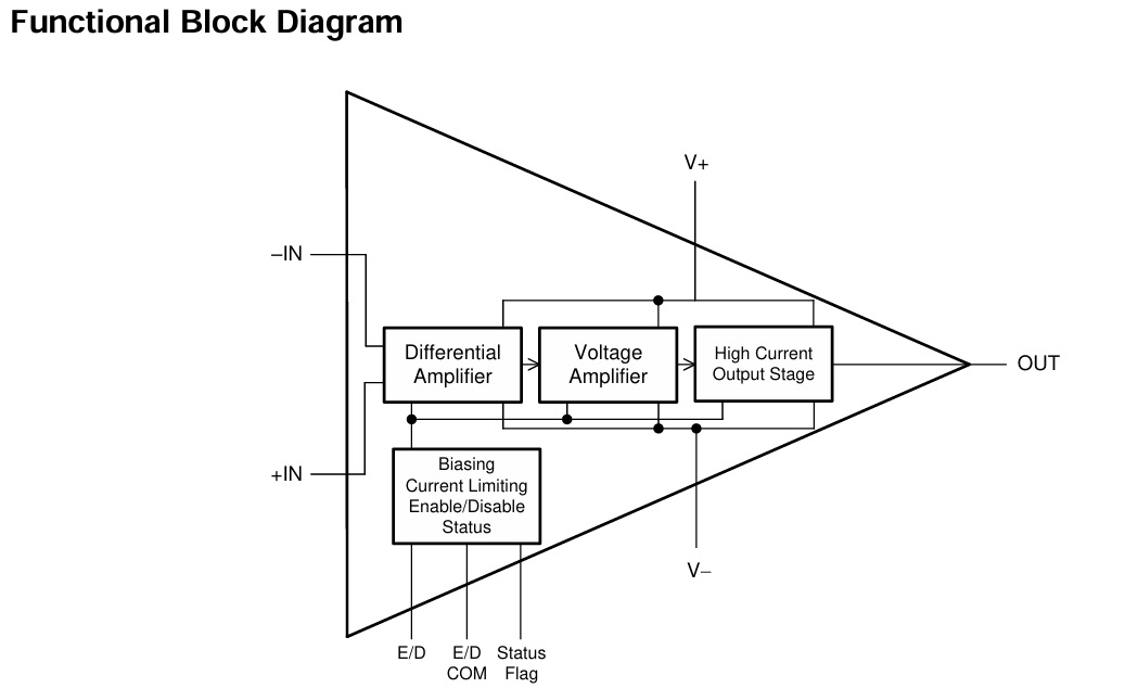
The OPA462 is a high voltage (180V) and high current drive (45 mA) operational amplifier. The device is unity-gain stable and has a gain-bandwidth product of 6.5 MHz The OPA462 is internally protected against over-temperature conditions and current overloads. The device is fully specified to perform over a wide power-supply range of ±6 V to ±90 V, or on a single supply of 12 V to 180 V. The status flag is an open-drain output that allows the device to be easily referenced to standard low-voltage logic circuitry. This high-voltage operational amplifier provides excellent accuracy and wide output swing, and is free from phase inversion problems that are often found in similar amplifiers. The output can be disabled using the enable-disable (E/D) pin. The E/D pin has a common return pin to allow for easy interface to low-voltage logic circuitry. This disable is accomplished without disturbing the input signal path, not only saving power but also protecting the load.
Status Flag Pin
The Status Flag pin indicates fault conditions and can be used in conjunction with the enable-disable function to implement fault control loops. This pin is triggered when the device enters an overtemperature or overcurrent fault condition. This pin is an open-drain, active-low output that allows the pin to be easily interfaced with standard low-voltage logic. The pin goes active if the junction temperature of the device rises to greater than 150°C, and resets after the device cools to 130°C. Additionally, the pin goes active if the device attempts to source more than the maximum continuous current of 30 mA. The status flag can be monitored from Pin 1 of CN2.
Thermal Protection
The OPA462 features internal thermal protection that is triggered when the junction temperature is greater than 150°C. When the protection circuit is triggered, thermal shutdown occurs to allow the junction to return a safe operating temperature. Thermal shutdown enables the Status Flag pin, which indicates the device has entered the thermal shutdown state.
Current Limit
Current limiting is accomplished by internally limiting the drive to the output transistors. The output can supply the limited current continuously, unless the die temperature rises to 150°C, which initiates thermal shutdown. With adequate heat dissipation, and use of the lowest possible supply voltage, the OPA462 can remain in current limit continuously without entering thermal shutdown. The best practice is to provide proper heat dissipation (either by a physical plate or by airflow) to remain well below the thermal shutdown threshold. For longest operational life of the device, keep the junction temperature below 125°C.
Enable and Disable
If left disconnected, E/D Com is pulled near V– (negative supply) by an internal 10-μA current source. When left floating, E/D is held approximately 2 V above E/D Com by an internal 1-µA source. Even though active operation of the OPA462 results when the E/D and E/D Com pins are not connected, a moderately fast, negative-going signal capacitively coupled to the E/D pin can overpower the 1-µA pullup current and cause device shutdown. This behaviour can appear as an oscillation and is encountered first near extreme cold temperatures. If the enable function is not used, a conservative approach is to connect E/D through a 30-pF capacitor to a low impedance source. Another alternative is the connection of an external current source from V+ (positive supply) sufficient to hold the enable level above the shutdown threshold. Figure 60 shows a circuit that connects E/D and E/D Com. The E/D Com pin is limited to (V–) + 100 V to enable the use of digital ground in a application where the OPA462 power supply is ±90 V. When the E/D pin is dropped to a voltage between 0 V and 0.65 V above the E/D Com pin voltage the output of the OPA462 will become disabled. While in this state the impedance of the output increases to approximately 160 kΩ. Because the inputs are still active, an input signal might be passed to the output of the amplifier. The voltage at the amplifier output is reduced because of a drop across this output impedance, and may appear distorted compared to a normal operation output. After the E/D pin voltage is raised to a voltage between 2.5 V and 5 V greater than the E/D Com, the output impedance returns to a normal state and the amplifier operates normally.
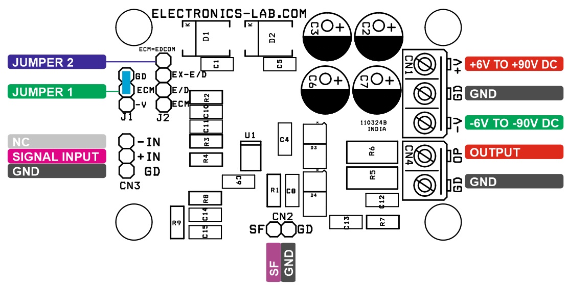
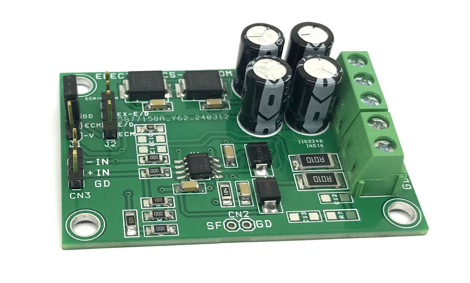
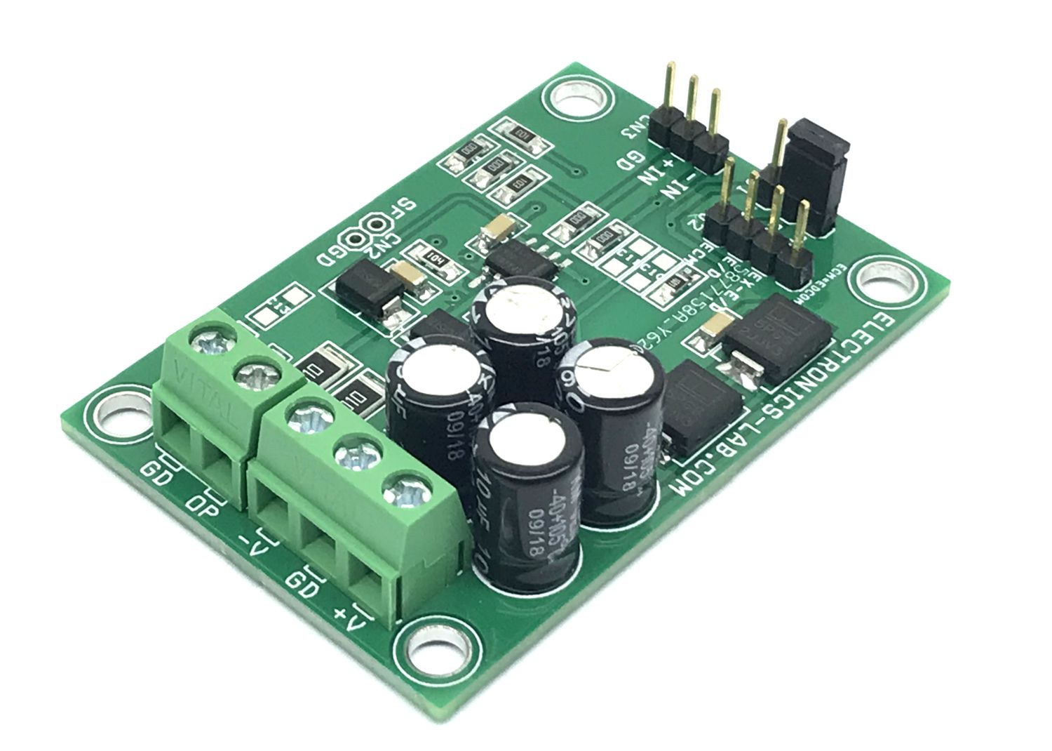
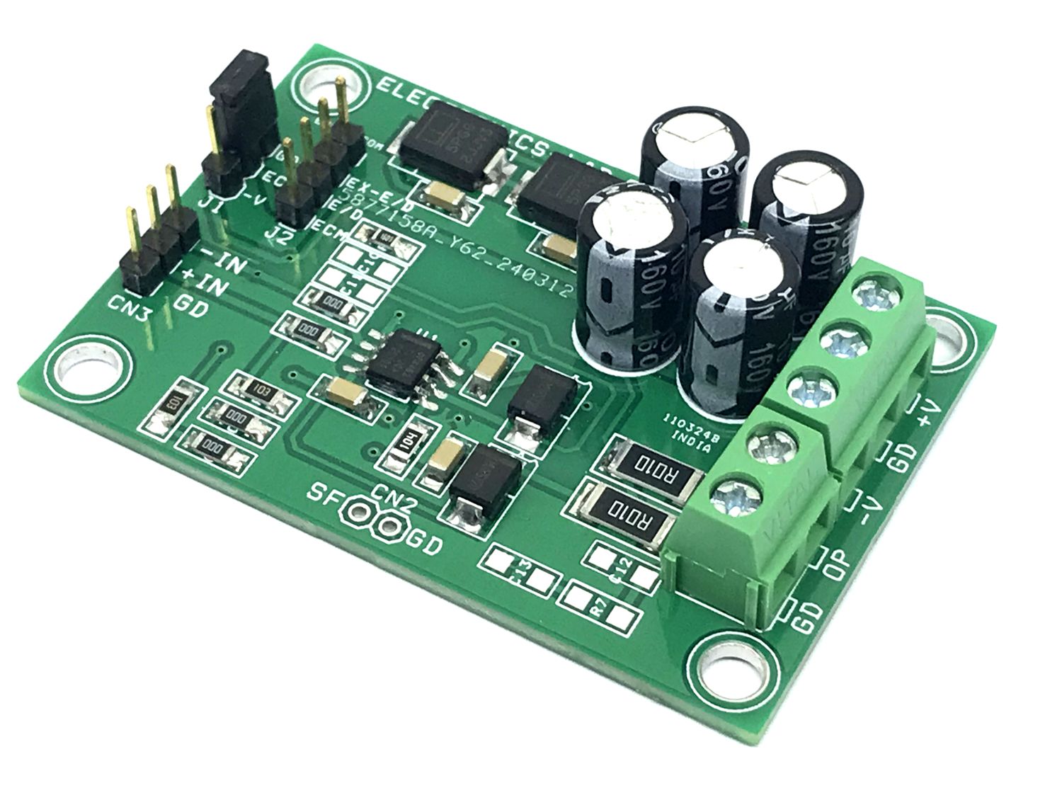
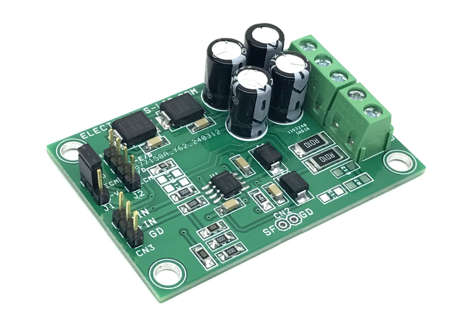
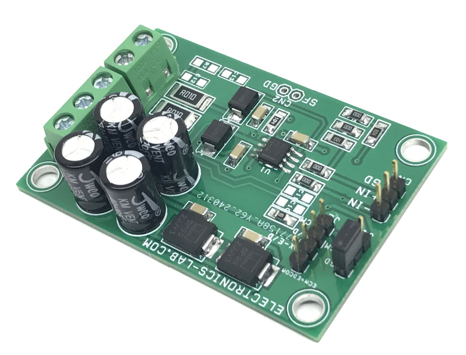
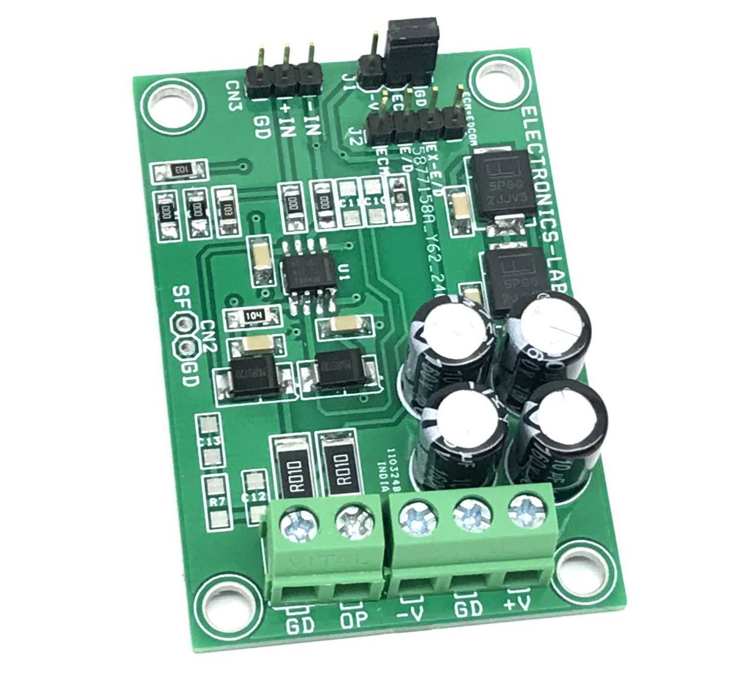
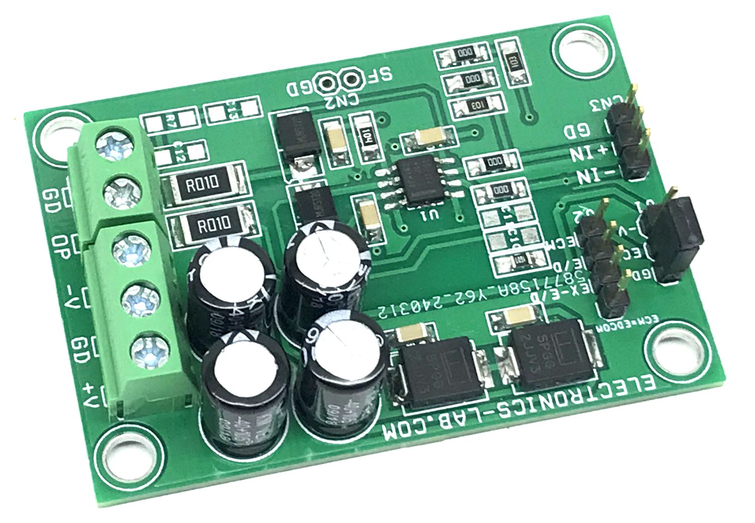
Connections
- CN1: Pin 1 = +6V to 90V DC Power, Pin 2 = GND, Pin 3 = -6V to -90V
- CN2: Pin 1 = SF (Fault Output), Pin 2 GND
- CN3: Pin 1 – Input (No Use for Non-Inverting Application), Pin 2 +Input Signal, Pin 3 = GND
- CN4: Pin 1 Output, Pin 2 GND
- J1: Jumper J1 and J2 Enable/Disable, enable = Connect EDCOM and GND, J2 Open
Schematic
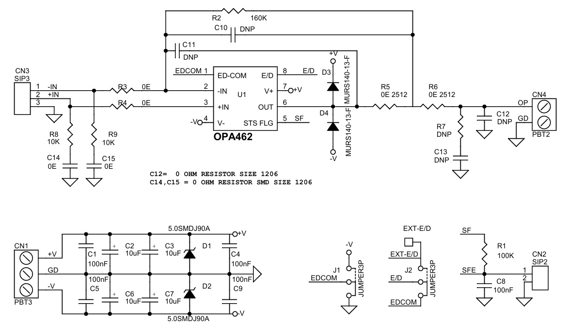
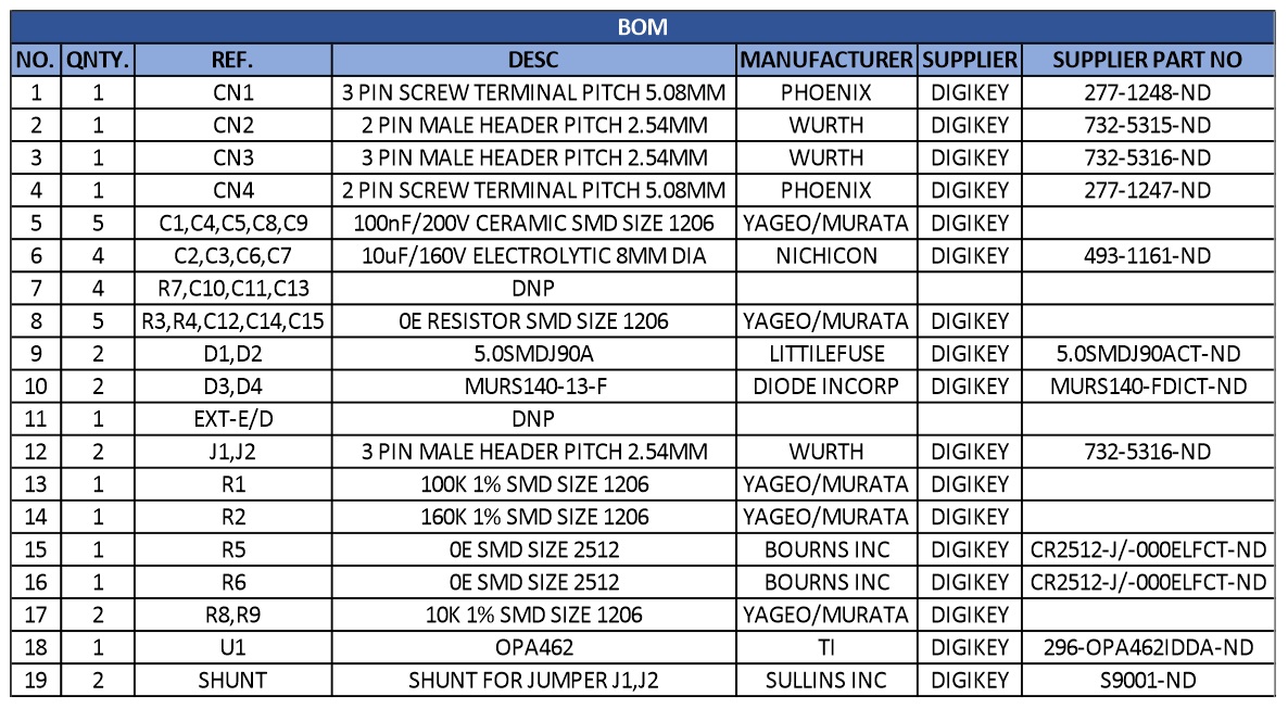
Parts List
| NO. | QNTY. | REF. | DESC | MANUFACTURER | SUPPLIER | SUPPLIER PART NO |
|---|---|---|---|---|---|---|
| 1 | 1 | CN1 | 3 PIN SCREW TERMINAL PITCH 5.08MM | PHOENIX | DIGIKEY | 277-1248-ND |
| 2 | 1 | CN2 | 2 PIN MALE HEADER PITCH 2.54MM | WURTH | DIGIKEY | 732-5315-ND |
| 3 | 1 | CN3 | 3 PIN MALE HEADER PITCH 2.54MM | WURTH | DIGIKEY | 732-5316-ND |
| 4 | 1 | CN4 | 2 PIN SCREW TERMINAL PITCH 5.08MM | PHOENIX | DIGIKEY | 277-1247-ND |
| 5 | 5 | C1,C4,C5,C8,C9 | 100nF/200V CERAMIC SMD SIZE 1206 | YAGEO/MURATA | DIGIKEY | |
| 6 | 4 | C2,C3,C6,C7 | 10uF/160V ELECTROLYTIC 8MM DIA | NICHICON | DIGIKEY | 493-1161-ND |
| 7 | 4 | R7,C10,C11,C13 | DNP | |||
| 8 | 5 | R3,R4,C12,C14,C15 | 0E RESISTOR SMD SIZE 1206 | YAGEO/MURATA | DIGIKEY | |
| 9 | 2 | D1,D2 | 5.0SMDJ90A | LITTILEFUSE | DIGIKEY | 5.0SMDJ90ACT-ND |
| 10 | 2 | D3,D4 | MURS140-13-F | DIODE INCORP | DIGIKEY | MURS140-FDICT-ND |
| 11 | 1 | EXT-E/D | DNP | |||
| 12 | 2 | J1,J2 | 3 PIN MALE HEADER PITCH 2.54MM | WURTH | DIGIKEY | 732-5316-ND |
| 13 | 1 | R1 | 100K 1% SMD SIZE 1206 | YAGEO/MURATA | DIGIKEY | |
| 14 | 1 | R2 | 160K 1% SMD SIZE 1206 | YAGEO/MURATA | DIGIKEY | |
| 15 | 1 | R5 | 0E SMD SIZE 2512 | BOURNS INC | DIGIKEY | CR2512-J/-000ELFCT-ND |
| 16 | 1 | R6 | 0E SMD SIZE 2512 | BOURNS INC | DIGIKEY | CR2512-J/-000ELFCT-ND |
| 17 | 2 | R8,R9 | 10K 1% SMD SIZE 1206 | YAGEO/MURATA | DIGIKEY | |
| 18 | 1 | U1 | OPA462 | TI | DIGIKEY | 296-OPA462IDDA-ND |
| 19 | 2 | SHUNT | SHUNT FOR JUMPER J1,J2 | SULLINS INC | DIGIKEY | S9001-ND |
Block Diagram
Connections
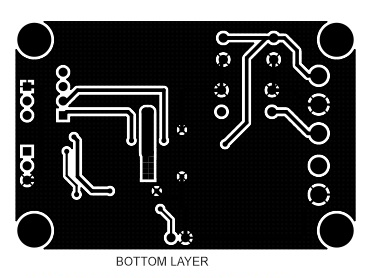
Gerber View
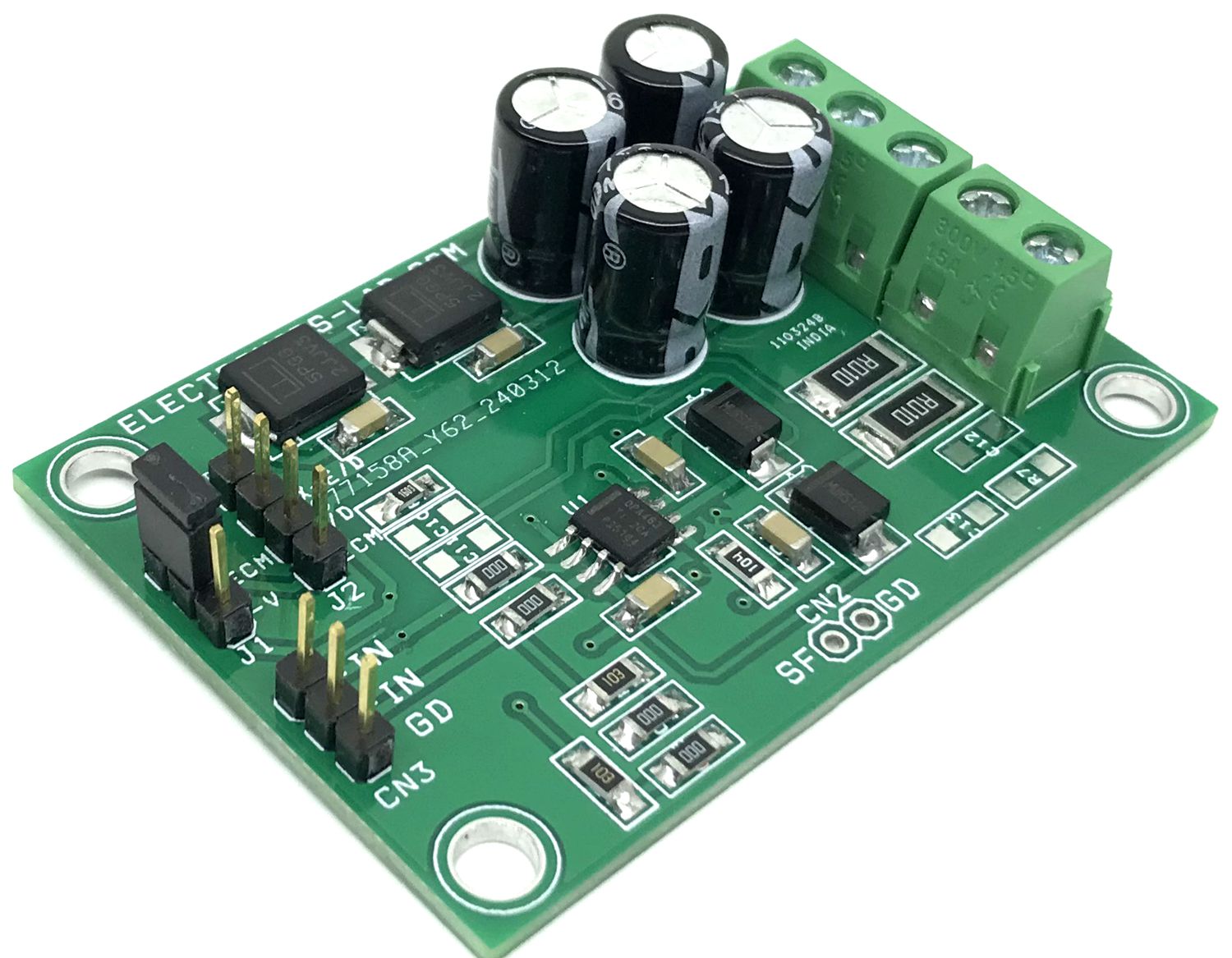
Photos
Video
OPA462 Datasheet
Please follow and like us:
PCB


Subscribe
Login
0 Comments


 Converter")
