

High Voltage 3-Phase Full-Wave PWM Brushless Motor Driver
- Rajkumar Sharma
- 116 Views
- advanced
- Tested
- SKU: EL148327
- Quote Now
- 0 Likes

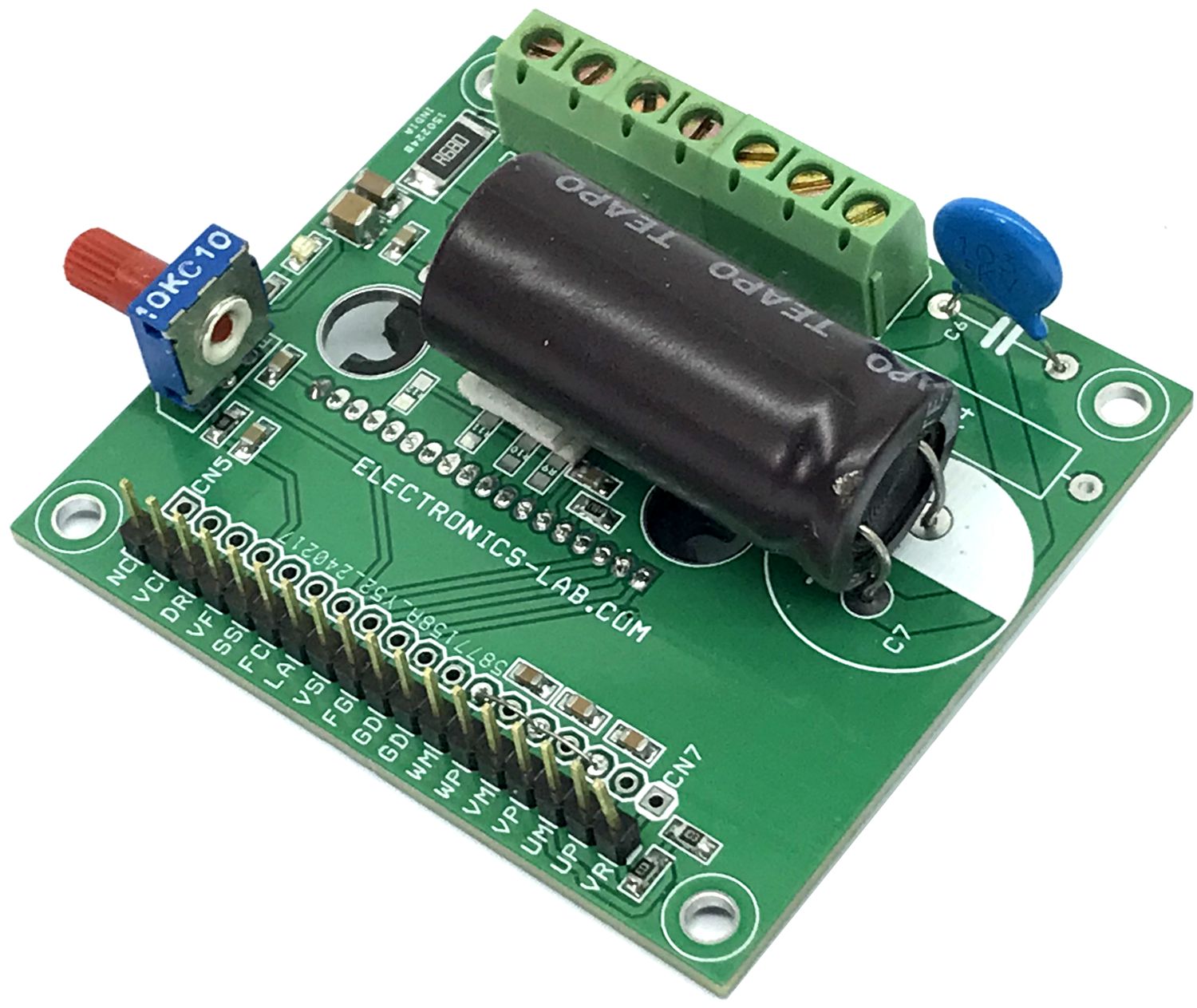
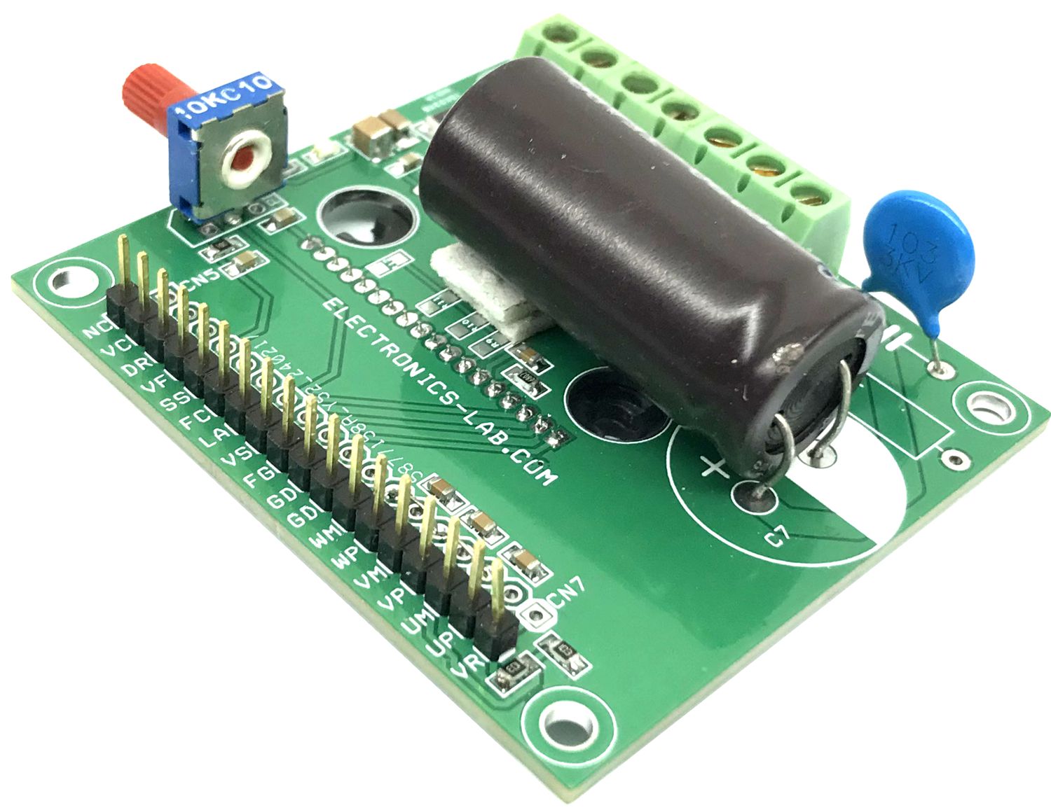
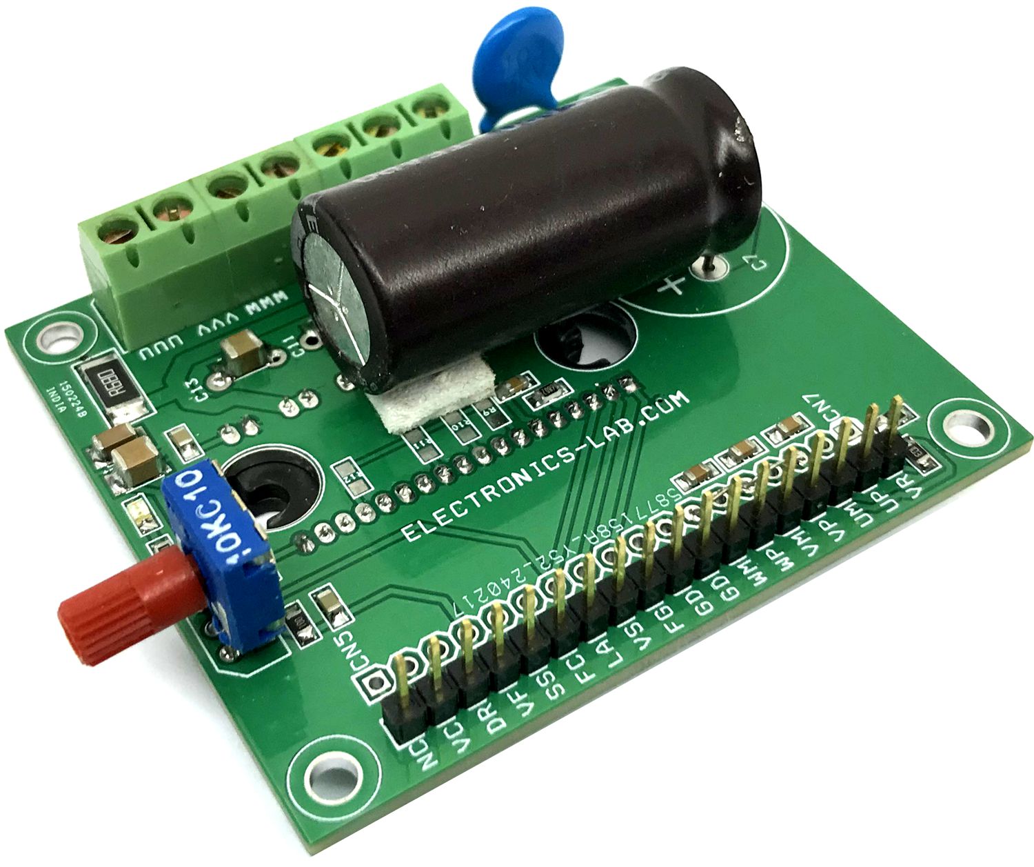
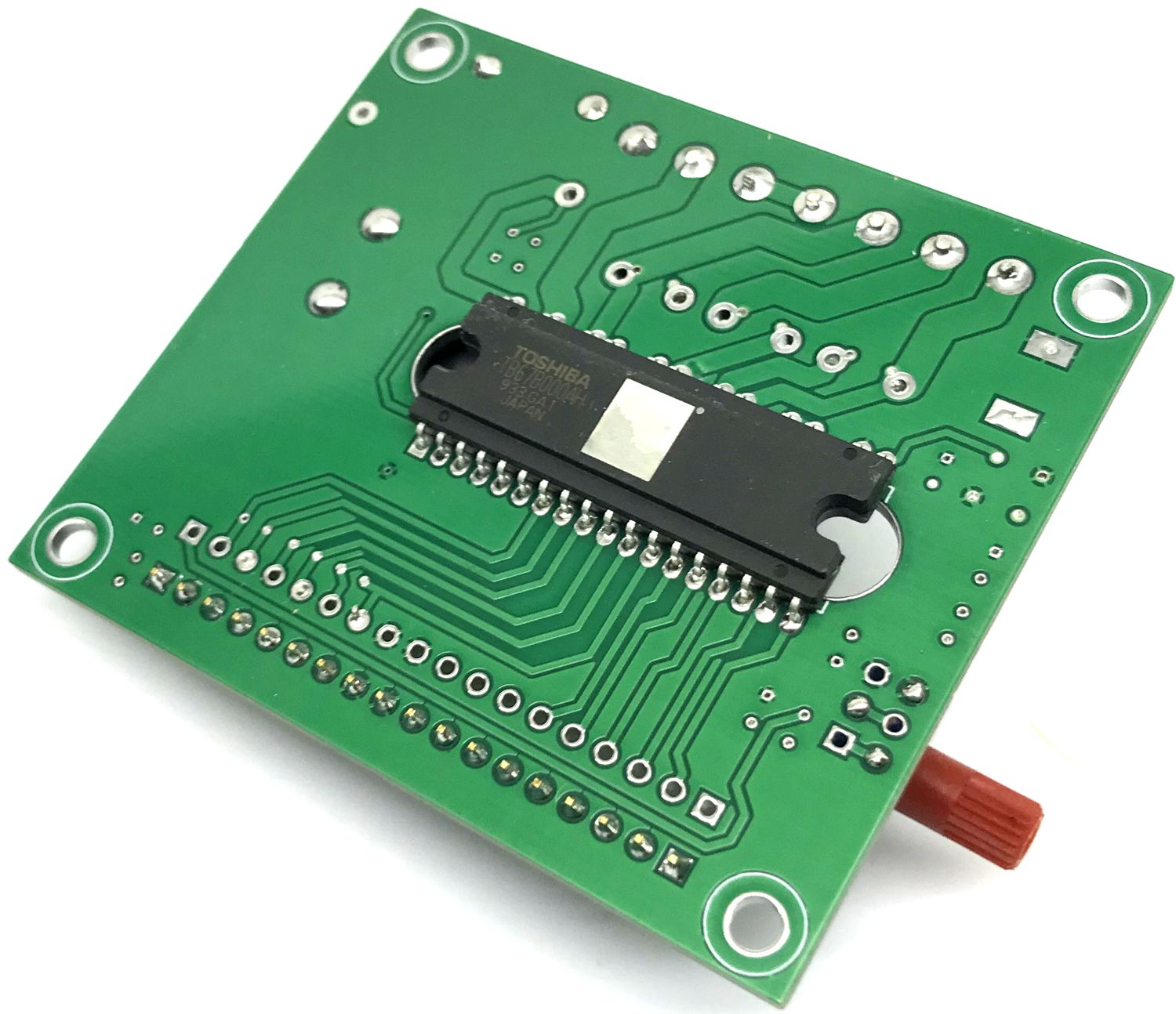
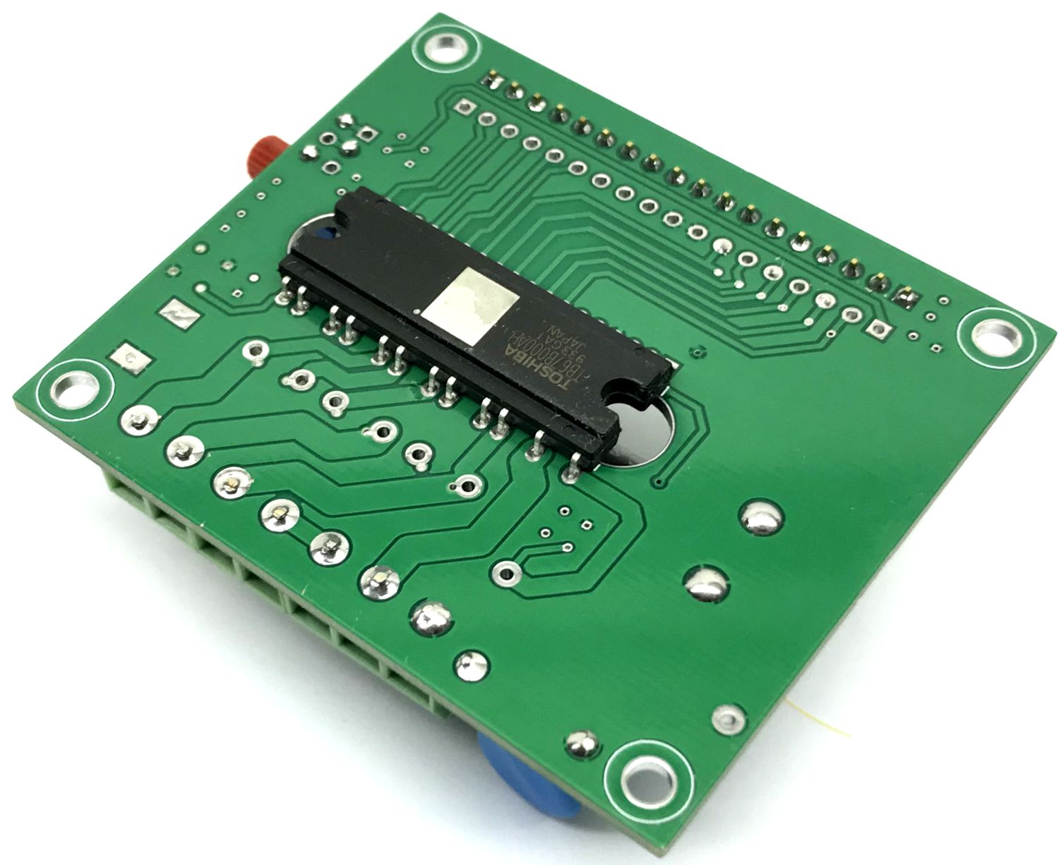
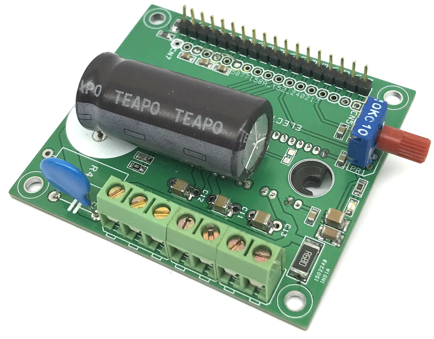
The project presented here is a three-phase sinewave PWM driver for high-voltage brushless motors. The board is built using TB67B000AHG chip, which is a high-voltage IC capable of handling 600V. The TB67B000AHG has a 2-in-1 (MCP) structure of controller (sine-wave PWM / wide-angle conduction) and a high-voltage driver. The rotation speed of a DC brushless motor can be controlled directly by the speed control signal (analog voltage) by an onboard trimmer potentiometer or from a microcontroller. The board supports a 3-phase BLDC motor with Hall sensors. On Board Trimmer, the potentiometer helps users to control the speed of the brushless motor.
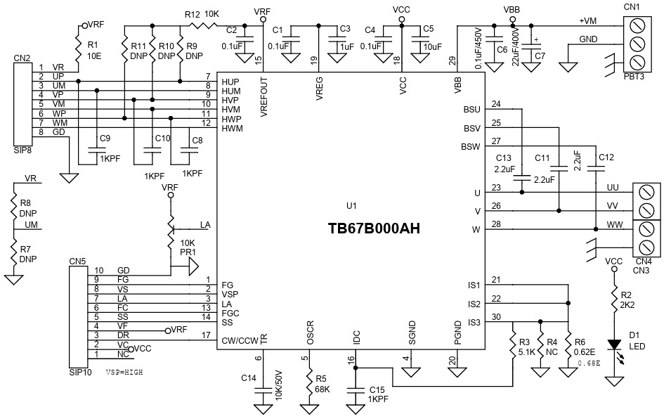
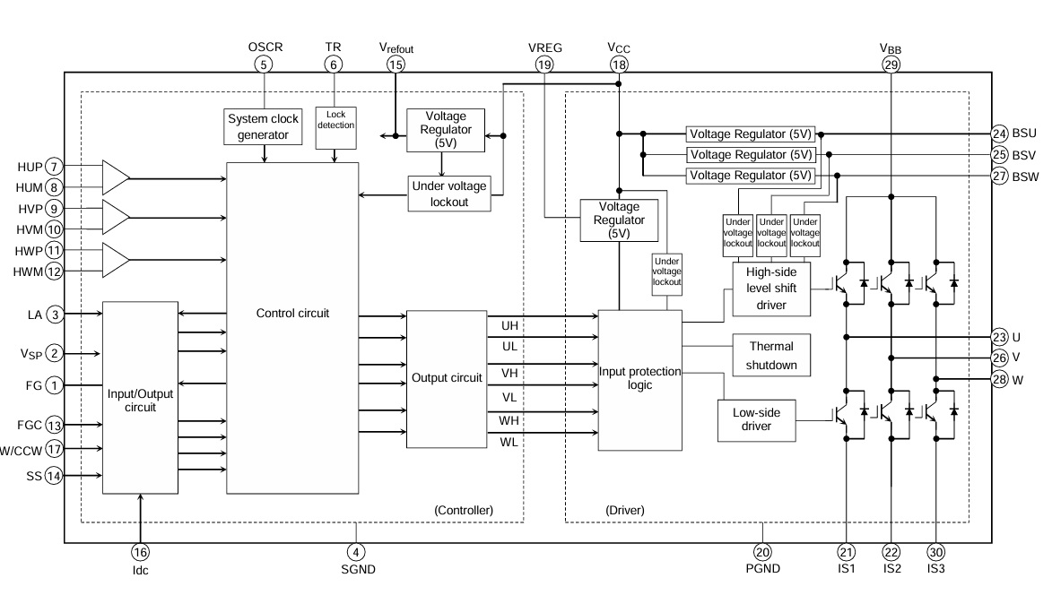
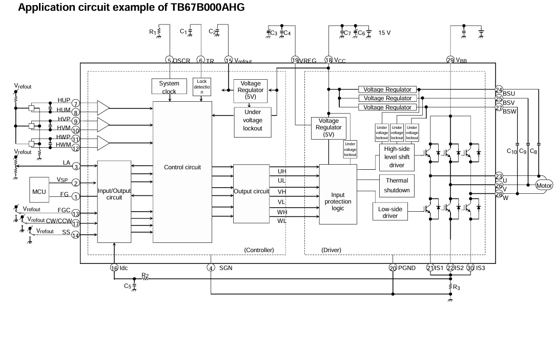
The TB67B000AHG is a high-voltage PWM brushless motor driver. The IC integrates a controller, which supports sinewave PWM drive with wide-angle commutation, and a high-voltage driver in a single package (“two-in-one”, i.e., MCP). It is designed to change the speed of a brushless motor directly.
Note 1: It is important to install a heatsink before conducting any test.
Note 2: The Driver supports a dual output hall sensor, for a single output hall sensor, Install R7 and R8 = 20K Ohms SMD size 0805, Tie UM, VM, WM pins of CN2. Use UP, VP, and WP Pins for 3 Hall sensors.
Note 3: The board operates at lethal voltages and has bulk capacitors that store significant charge. Accidental contact can lead to lab equipment damage, personnel injury, and may be fatal. Please be exceptionally careful when probing and handling this board. Always observe normal laboratory precautions.
Note 4: Since the board operates at lethal voltages, use a plastic shaft for the trimmer potentiometer. Avoid metal shaft potentiometer.
Features
- Operating power supply voltage range: VCC = 13.5 to 16.5 V
- Motor power supply operating voltage range: VBB = 50 to 420 V (Up to 450V, Limited due to Capacitor Voltage)
- A Controller and a high-voltage driver integrated in a single package.
- Sine-wave PWM drive or wide-angle commutation drive is selectable.
- Built-in oscillator circuit (carrier frequency = fosc/252 (Hz))
- Bootstrap circuitry: Built-in bootstrap diode
- Built-in overcurrent protection, thermal shutdown, undervoltage lockout, and motor-lock detection.
- Internal voltage regulator circuit (VREG = 5 V (typ.), 30 mA (max), Vrefout = 5 V (typ.), 35 mA (max))
- PCB Dimensions 64.77 x 57.15 mm
- 4 x 3.2 mm Mounting Holes
- 2 x 8 mm Holes for Heat-Sink
Sequence of power supply
Sequence of power supply: Please supply the power by following the procedure of (1) to (3).
- Apply power supply of VCC. (Power Supply for Controller Chip)
- In applying Vcc, connect Vsp to GND or open. (VSP=VS On PCB)
- In case terminals of CW/CCW, LA, and SS are controlled by signals of external IC, connect them to GND or open. After applying power supply of VCC, set the terminal of CW/CCW, LA, and SS high-level if needed.
- Apply power supply of VBB. (Motor Power)
- Apply voltage to Vsp.
Sequence of power shutdown: Please shut down the power by following procedures of (1) to (3).
- Set Vsp to 0V. ( VSP=VS on PCB)
- In case terminals of CW/CCW, LA, and SS are controlled by signals of external IC
- After setting Vsp 0V, connect them to GND or open. (VSP=VS On PCB)
- Shut down VBB.
- Shut down VCC.
Output current
The absolute maximum rating is 2 A which must not be exceeded, even for a moment. Design an actual application system with the IC so as not to make the inrush current and the lockout current exceed the absolute maximum ratings, especially when a motor starts up and gets stuck in the lockout. The available output current depends on the usage conditions(ambient temperature, mounting board method, and so on). Design an actual application system with a sufficient margin in order that Tj does not exceed 150°C.
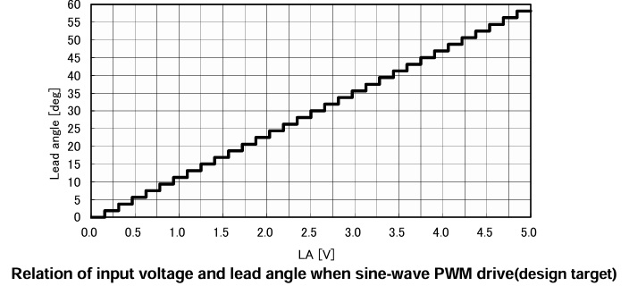
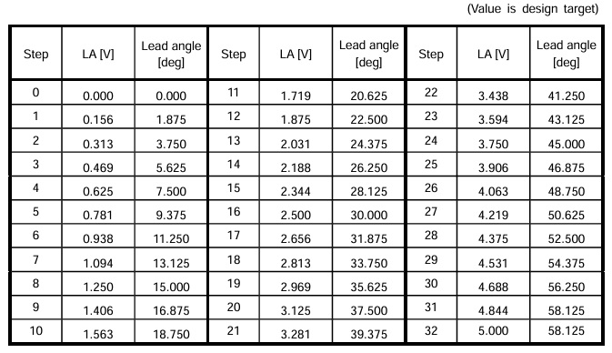
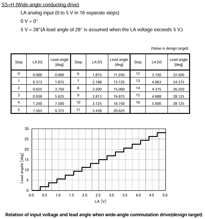
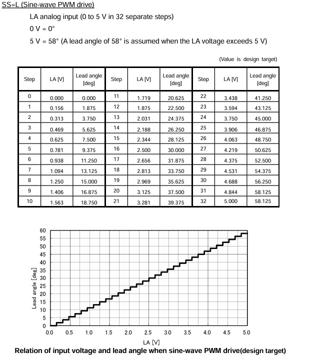
Lead angle control
The lead angle of the driver output according to the induced voltage can be adjusted by the input voltage of LA terminal. The range of lead angle is as follows; Sine-wave PWM drive: 0° to 58°, Wide-angle conducting drive: 0°to 28° The efficiency of the motor operation can be improved by adjusting the lead angle. In adjusting the motor characteristics by applying the lead angle, change the lead angle by LA terminal and compare the motor current. Adjust the voltage of the LA terminal in order to minimize the motor current as comparing the motor current before and after changing the lead angle under the condition that the rotation speed is the same.
SS=L (Sine-wave PWM drive)
LA analog input (0 to 5 V in 32 separate steps) 0 V = 0° 5 V = 58° (A lead angle of 58° is assumed when the LA voltage exceeds 5 V)
Oscillator Frequency (Default 20Khz = R5 68K Ohms, If R5 is 75K Ohms Frequency 18Khz)
Oscillation frequency (Fosc) range should be 3.5MHz to 6.4MHz. The relation of the oscillation frequency (Fosc) and the PWM frequency (FC) is as follows; FC=Fosc/252. When R1= 68kΩ, FC=20 kHz (typ.), and when R1= 75kΩ, FC=18 kHz (typ.).
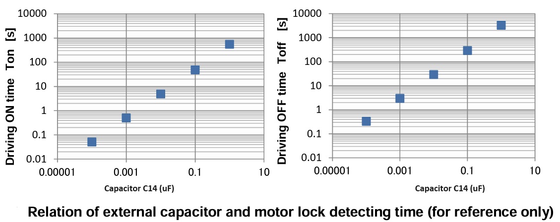
TR terminal
When the motor is locked, the motor lock detection operates and the drive output is turned on and off (intermittent operation). Driving OFF period (Toff) and driving ON period (Ton) can be configured by the external capacitor (C1) of TR terminal. When this function is not used, please connect this terminal to SGND. The relation of external capacitor (C14) and driving ON/OFF period is roughly calculated as follows. ・
Setting time
- Driving ON period Ton[s]=C1×(VH―VL) ×2/I×500 counters
- Driving OFF period Toff[s]=C1×(VH―VL) ×2/I×3000 counters
- When C14 = 0.01μF, I = 3μA (typ.), VH= 2 V (typ.) and VL= 0.5V (typ.), and so
- Ton[s]=5s (typ.) and Toff[s]=30s (typ.)
Current Sense Resistor
The relation between the output current (IOUT) and the detecting resistor (R6) is provided roughly in the following formula. IOUT = Vdc/ R6 Voltage of current detection Vdc: 0.475V (min.), 0.5 V (typ.), and 0.525V (max.) Example) When the resistor (R6) is configured 0.51 Ω, IOUT (typ.) = 0.5 V (typ.)/0.51 Ω ∼ − 0.98 A Please determine the rating of the external parts with sufficient margins because large current flows in the detecting resistor (R6). In operating the motor, the power on the detecting resistor (P) is calculated as follows; P=0.525Vx0.525V/ R6 (max.). For example, when R6=0.51Ω, P=0.540W. So, please apply the resistor of 1 W or more as a rated power.
VSP Pin ( On PCB VSP=VS)
Operation and stop of the motor and rotating speed can be controlled by inputting command signal of the output ON duty to Vsp terminal. Please input analog voltage as a command signal. Moreover, when rotation speed needs to be controlled, connect it to MCU with Vsp signal and FG signal and feedback the speed to control the motor rotation number.
FG Pin
Push-pull circuit of 5V output is constructed. When rotation speed needs to be controlled, input FG signal to MCU to use this signal as the information of the motor rotating number.
CW/CCW Pin
In using this terminal by fixing the voltage of the terminal, connect it to Vrefout or SGND. In connecting to Vrefout, it becomes high level. In connecting to SGND, it becomes low level. In using this terminal by inputting the external control signal, input this signal after applying the power supply of Vcc. In shut down, turn off Vcc after the control signal is turned off. In switching the logic of CW/CCW terminal, change the input signal after setting the Vsp terminal 0.7V or less and turning off the operation output. After switching the input signal, start the motor operation by Vsp terminal.
FGC Pin
In using this terminal by fixing the voltage of the terminal, connect it to Vrefout, SGND or Vrefout/2. In connecting to Vrefout, it becomes high level. In connecting to Vrefout /2, it becomes M level. And in connecting to SGND, it becomes low level. In using this terminal by inputting the external control signal, input this signal after applying the power supply of Vcc. In shut down, turn off Vcc after the control signal is turned off.
SS Pin
In using this terminal by fixing the voltage of the terminal, connect it to Vrefout or SGND. In connecting to Vrefout, it becomes high level. In connecting to SGND, it becomes low level. In using this terminal by inputting the external control signal, input this signal after applying the power supply of Vcc. In shut down, turn off Vcc after the control signal is turned off.
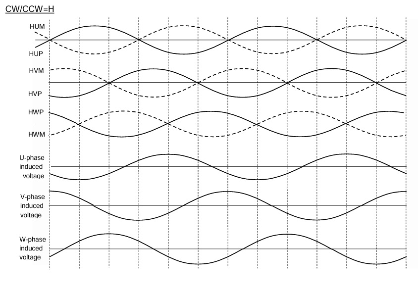
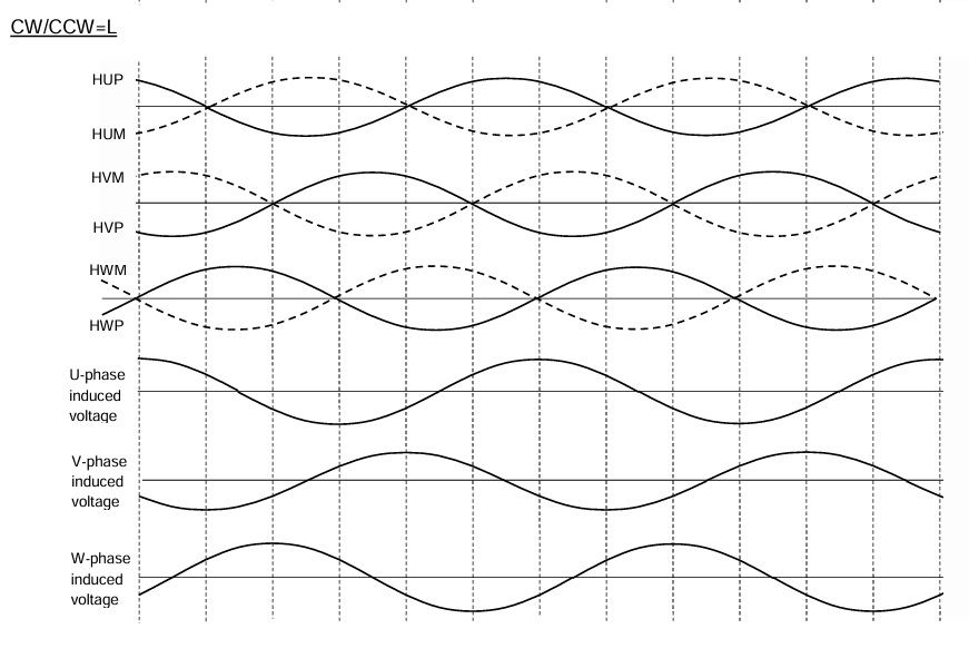
HUP, HUM, HVP, HVM, HWP, HWM Pins
Input hall signals to HUP, HUM, HVP, HVM, HWP, and HWM terminals. Select hall elements or hall ICs to provide hall signals. Connect output terminals of U, V, and W, and the hall signal terminals of HUP, HUM, HVP, HVM, HWP, and HWM, to the motor to have the relation shown in the timing chart of “ refer timing chart). Notes in using the motor”. ・If 5V is supplied from the Vrefout power supply to the hall elements, add the limiting resistor to the power supply terminal of the hall element in order to be within the maximum input current of the hall element. ・To recognize switching of the hall signal correctly, the amplitude of the hall elements should be 40 mV or more and the input voltage range should be 0.5 V to 4.0 V. ・Hall amplifier has a hysteresis. When the amplitude of it is small, the phase gap of the switching timing becomes large. So, please make the amplitude of it as large as possible. ・When the capacitor for reducing the noise of the hall signal is attached, please arrange it close to HUP and HUM terminals, HVP and HVM terminals, and HWP and HWM terminals. The recommended capacitor is 0.001 μF to 0.1 μF.
< Notes in using the hall IC> Please configure HUP, HVP, HWP, HUM, HVM, and HWM as follows. It is recommended to adopt low-pass filter between the input terminal and SGND to reduce the noise. However, in this case, delay time of the input signal should be considered.
- HUP, HVP, and HWP: Input voltage: H level = Vrefout, L level = SGND HUM, HVM, and HWM: Input voltage: Vrefout/2 * Configure it with resistive dividing voltage between Vrefout terminal and SGND.
- HUP, HVP, and HWP: Input voltage: Vrefout/2 * Configure it with resistive dividing voltage between Vrefout terminal and SGND. HUM, HVM, and HWM: Input voltage: H level = Vrefout, L level = SGND
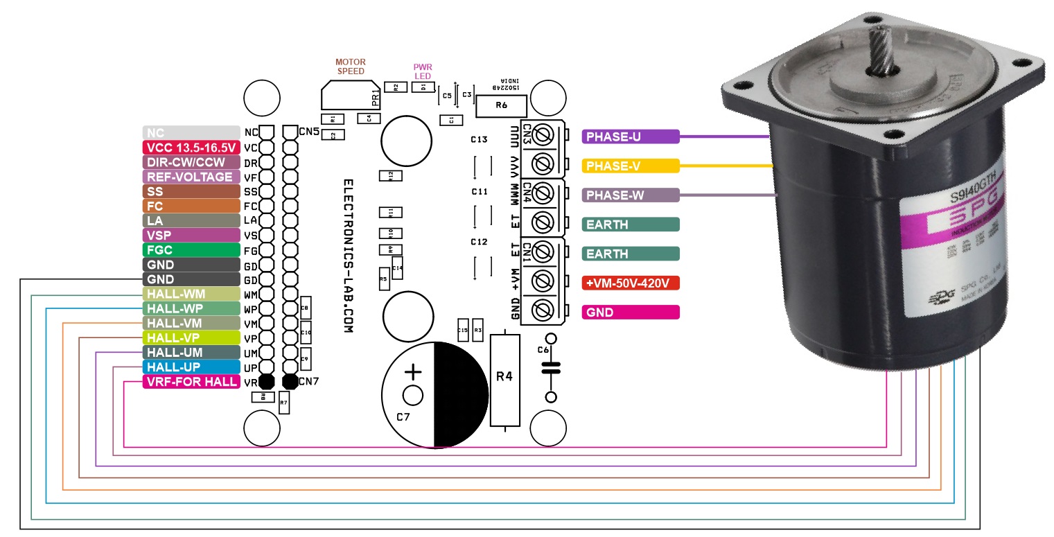
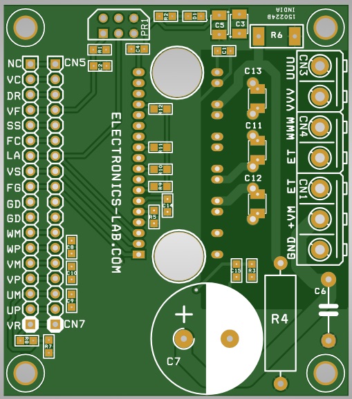
Connections
- CN1: Pin1 = +VM Motor Supply 50V to 420V DC, Pin 2 = GND, Pin 3 = GND
- CN2: Pin 1 Reference 5V for Hall Sensor, Pin 3=Hall Sensor HUP, Pin 4 = Hall Sensor HUM, Pin 5 = Hall Sensor HVP, Pin 6 = Hall Sensor HVM, Pin 6 = Hall Sensor HWP, Pin 7 = Hall Sensor HWM, Pin 8 = GND
- CN3: Pin 1 = Motor W Phase, Pin 2 = Earth
- CN4: Pin 1 = Motor U Phase, Pin 2 = Motor V Phase
- CN5: Pin 1 = NC, Pin 2 = VCC 13.5V to 16.5V, Pin 3 = Dir CW/CCW (High or Low), Pin 4 = VREF 5V DC, Pin 5 = SS, Pin 6 = FGC, Pin 7 = LA Speed Control Voltage Input, Pin 8 = VSP, Pin 9 = FG, Pin 10 = GND
- D1: Power LED
- PR1: Trimmer Potentiometer for Speed Control
Schematic
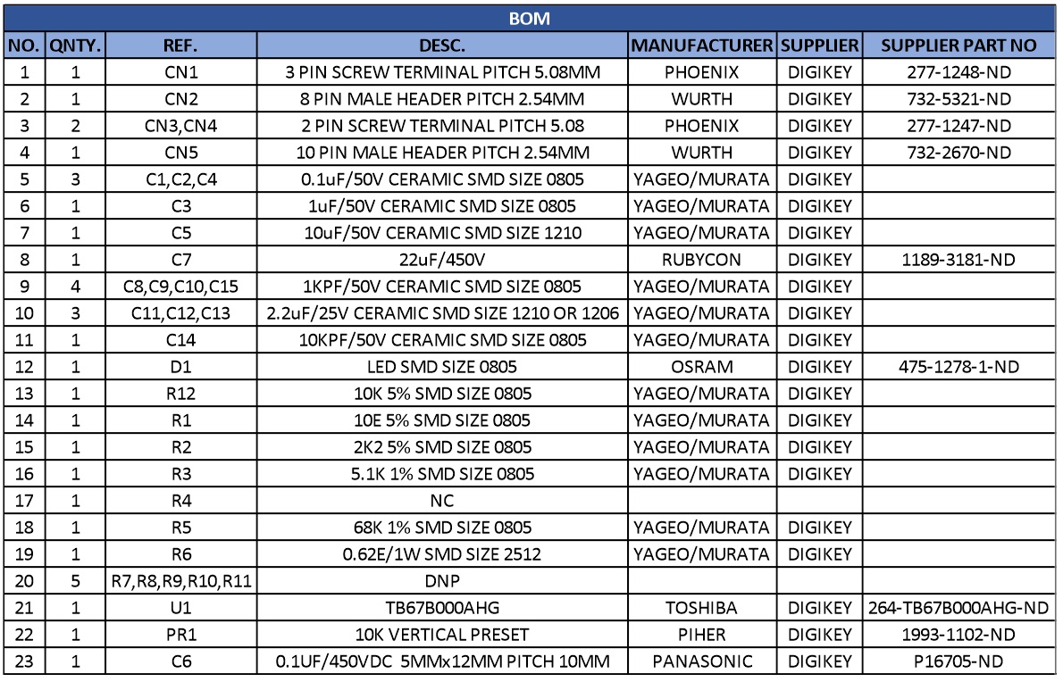
Parts List
| NO. | QNTY. | REF. | DESC. | MANUFACTURER | SUPPLIER | SUPPLIER PART NO |
|---|---|---|---|---|---|---|
| 1 | 1 | CN1 | 3 PIN SCREW TERMINAL PITCH 5.08MM | PHOENIX | DIGIKEY | 277-1248-ND |
| 2 | 1 | CN2 | 8 PIN MALE HEADER PITCH 2.54MM | WURTH | DIGIKEY | 732-5321-ND |
| 3 | 2 | CN3,CN4 | 2 PIN SCREW TERMINAL PITCH 5.08 | PHOENIX | DIGIKEY | 277-1247-ND |
| 4 | 1 | CN5 | 10 PIN MALE HEADER PITCH 2.54MM | WURTH | DIGIKEY | 732-2670-ND |
| 5 | 3 | C1,C2,C4 | 0.1uF/50V CERAMIC SMD SIZE 0805 | YAGEO/MURATA | DIGIKEY | |
| 6 | 1 | C3 | 1uF/50V CERAMIC SMD SIZE 0805 | YAGEO/MURATA | DIGIKEY | |
| 7 | 1 | C5 | 10uF/50V CERAMIC SMD SIZE 1210 | YAGEO/MURATA | DIGIKEY | |
| 8 | 1 | C7 | 22uF/450V | RUBYCON | DIGIKEY | 1189-3181-ND |
| 9 | 4 | C8,C9,C10,C15 | 1KPF/50V CERAMIC SMD SIZE 0805 | YAGEO/MURATA | DIGIKEY | |
| 10 | 3 | C11,C12,C13 | 2.2uF/25V CERAMIC SMD SIZE 1210 OR 1206 | YAGEO/MURATA | DIGIKEY | |
| 11 | 1 | C14 | 10KPF/50V CERAMIC SMD SIZE 0805 | YAGEO/MURATA | DIGIKEY | |
| 12 | 1 | D1 | LED SMD SIZE 0805 | OSRAM | DIGIKEY | 475-1278-1-ND |
| 13 | 1 | R12 | 10K 5% SMD SIZE 0805 | YAGEO/MURATA | DIGIKEY | |
| 14 | 1 | R1 | 10E 5% SMD SIZE 0805 | YAGEO/MURATA | DIGIKEY | |
| 15 | 1 | R2 | 2K2 5% SMD SIZE 0805 | YAGEO/MURATA | DIGIKEY | |
| 16 | 1 | R3 | 5.1K 1% SMD SIZE 0805 | YAGEO/MURATA | DIGIKEY | |
| 17 | 1 | R4 | NC | |||
| 18 | 1 | R5 | 68K 1% SMD SIZE 0805 | YAGEO/MURATA | DIGIKEY | |
| 19 | 1 | R6 | 0.62E/1W SMD SIZE 2512 | YAGEO/MURATA | DIGIKEY | |
| 20 | 5 | R7,R8,R9,R10,R11 | DNP | |||
| 21 | 1 | U1 | TB67B000AHG | TOSHIBA | DIGIKEY | 264-TB67B000AHG-ND |
| 22 | 1 | PR1 | 10K VERTICAL PRESET | PIHER | DIGIKEY | 1993-1102-ND |
| 23 | 1 | C6 | 0.1UF/450VDC 5MMx12MM PITCH 10MM | PANASONIC | DIGIKEY | P16705-ND |
Connections
Block Diagram
Application Example
 Working Waveforms
Motor Lock Detection Time
Relation LA 0 to 5V and PWM Steps
Sinewave PWM Steps
When SS=High
When SS=Low
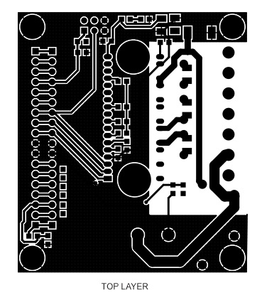
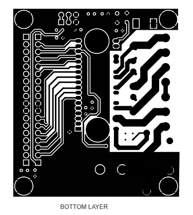
Gerber View
Photos

Video
TB67B000AHG Datasheet
Please follow and like us:
PCB


Subscribe
Login
0 Comments


")