Isolated, Single-Channel RS232 transceiver (Isolated RS232 to UART)
- Rajkumar Sharma
- 4.082 Views
- easy
- Tested
- SKU: EL103130
- Quote Now
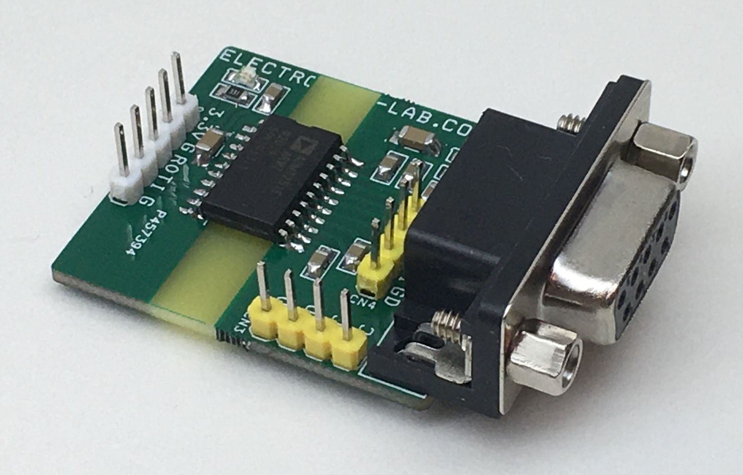
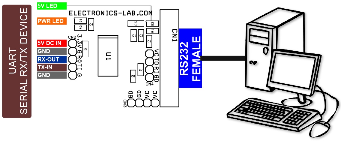
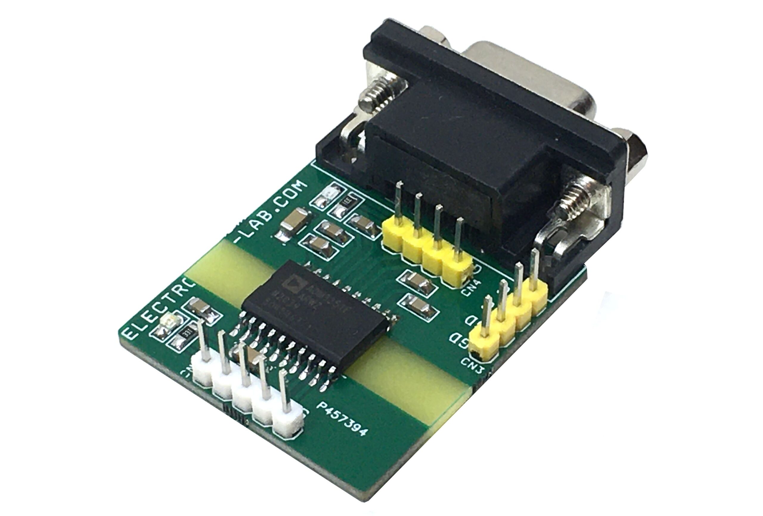
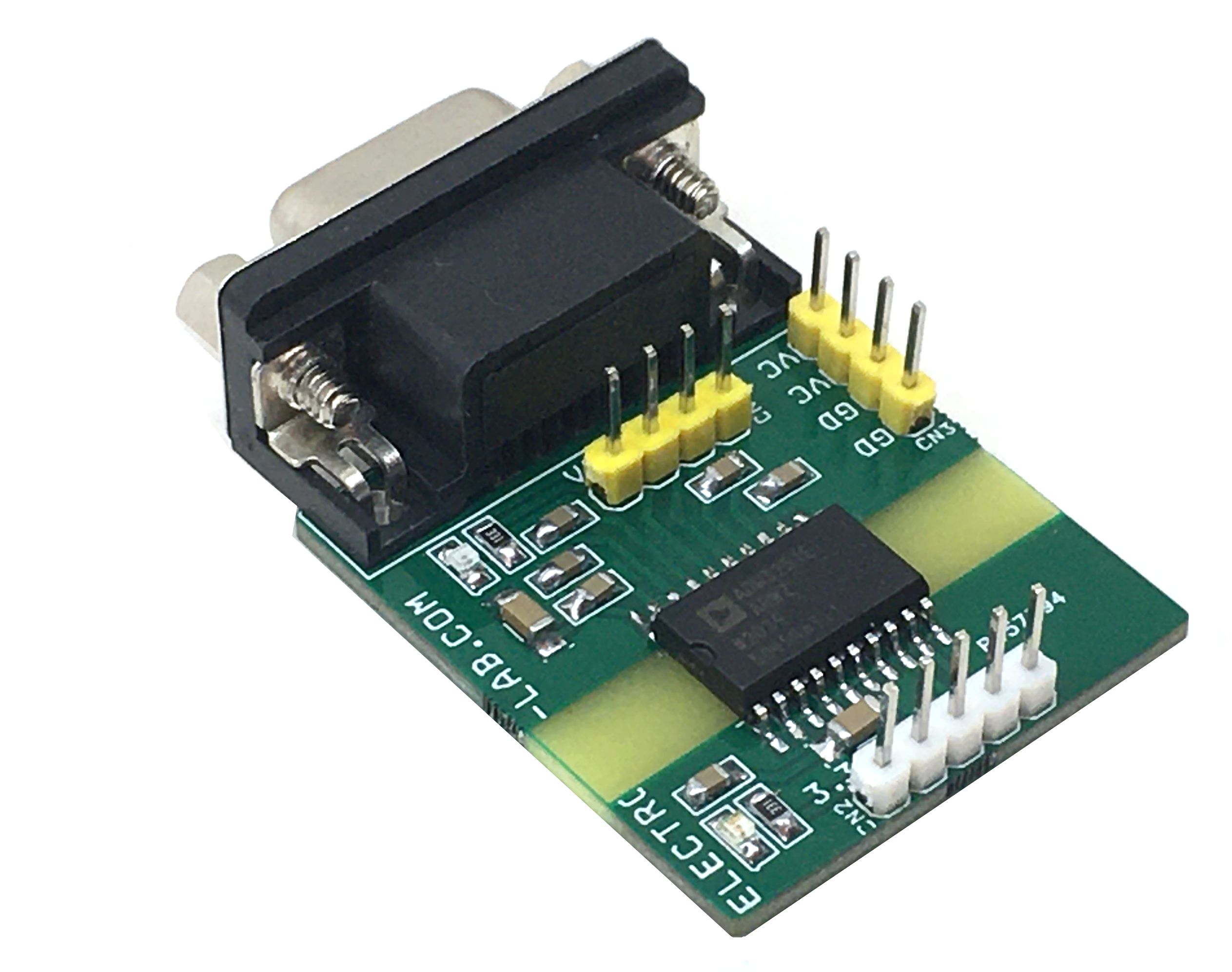
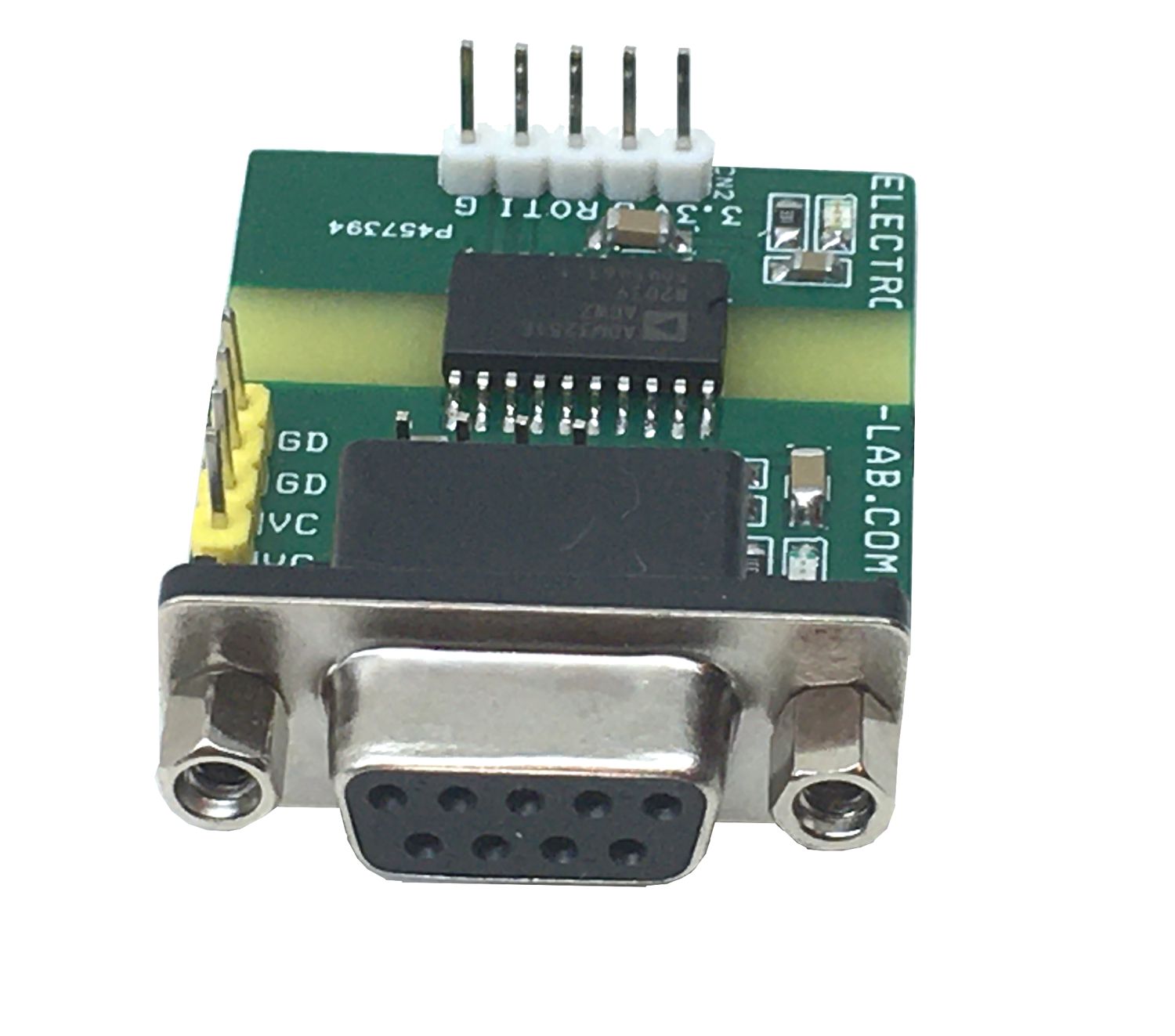
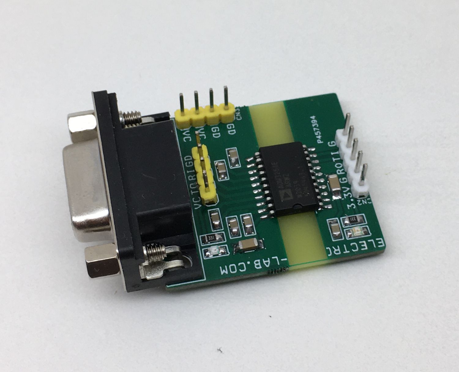
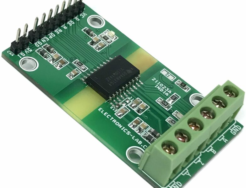
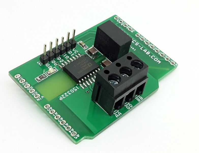
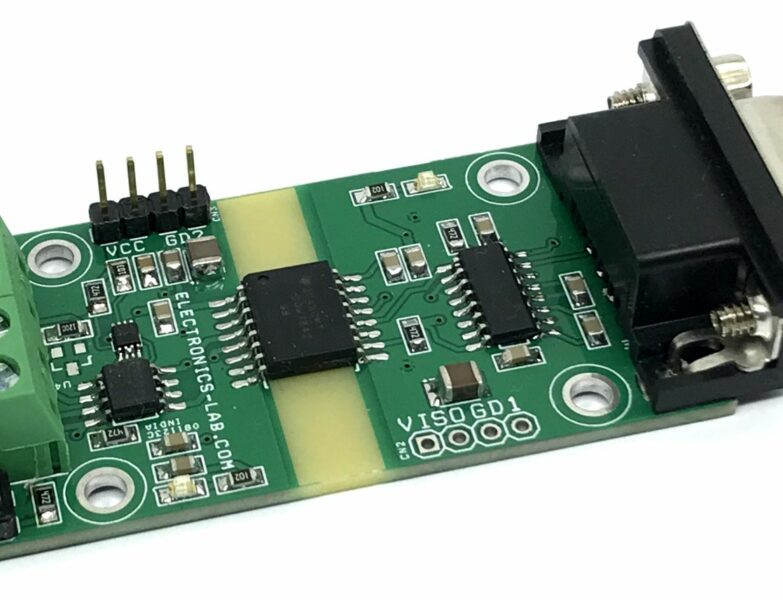
The project presented here provides an isolated interface between the RS-232 cable network and the connected UART systems to protect against voltage spikes and ground loops within the noisy environment and improve system reliability. The project achieves a robust data communication link in harsh industrial environment. ADM3251E chip from Analog Devices is the heart of the project, this chip is a high speed, 2.5KV fully isolated, single-channel RS-232 transceiver device that operates from a single 5 V power supply. Due to the high ESD protection on the RIN and TOUT pins, the device is ideally suited for operation in electrically harsh environments or where RS-232 cables are frequently being plugged and unplugged. Four external 0.1 μF charge pump capacitors are used for the voltage doubler/inverter, permitting operation from a single 5 V supply. Project operates at data rates up to 460kbps. RS-232 transceiver D-Sub 9 Pin Female block provide convenient signal connections. D2 Power LEDs on respective isolation ends. The chip has inbuilt isolated DC-DC Converter thus the project can work with single supply. Apply 5V DC to CN2 and project is ready to go.
Features
- Supply 5V DC CN2 Single Supply Operations
- CN4 RS232 Aux
- 9 Pin D-Type Female Connector for RS232 Interface (CN1)
- 5 Pin Male Header Connector for UART Interface (CN2)
- 5KV Fully isolation
- Data Rates Up to 460kbps
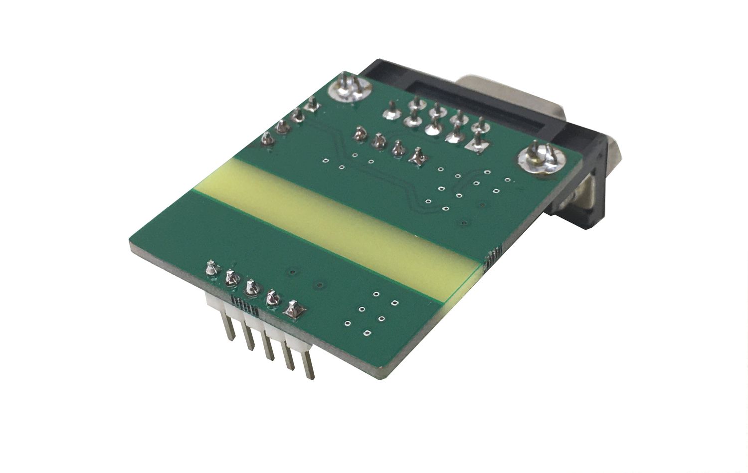
- PCB DIMENSIONS: 35.88 x 31.91mm
5.0 V LOGIC TO TIA-232E TRANSMITTER
The transmitter driver converts the 5.0 V logic input levels into RS-232 output levels. When driving an RS-232 load with VCC = 5.0 V, the output voltage swing is typically ±10 V.
TIA-232E TO 5 V LOGIC RECEIVER
The receiver is an inverting level-shifter that accepts the RS-232 input level and translates it into a 5.0 V logic output level. The input has an internal 5 kΩ pull-down resistor to ground and is also protected against overvoltage of up to ±30 V. An unconnected input is pulled to 0 V by the internal 5 kΩ pull-down resistor. This, therefore, results in a Logic 1 output level for an unconnected input or for an input connected to GND. The receiver has a Schmitt-trigger input with a hysteresis level of 0.1 V. This ensures error-free reception for both a noisy input and for an input with slow transition times.
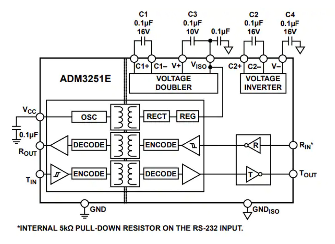
Internal Diagram
HIGH BAUD RATE
The Project offers high slew rates, permitting data trans-mission at rates well in excess of the TIA-232E specifications. The RS-232 voltage levels are maintained at data rates up to 460 kbps.
Inbuilt DC-DC Converter Enable/Disable
The ADM3251E incorporates a dc-to-dc converter section, which works on principles that are common to most modern power supply designs. VCC power is supplied to an oscillating circuit that switches current into a chip-scale air core transformer. Power is transferred to the secondary side, where it is rectified to a high dc voltage. The power is then linearly regulated to about 5.0 V and supplied to the secondary side data section and to the VISO pin. The VISO pin should not be used to power external circuitry.
Because the oscillator runs at a constant high frequency independent of the load, excess power is internally dissipated in the output voltage regulation process. Limited space for transformer coils and components also adds to internal power dissipation. This results in low power conversion efficiency.
The ADM3251E can be operated with the dc-to-dc converter enabled or disabled. The internal dc-to-dc converter state of the ADM3251E is controlled by the input VCC voltage. In normal operating mode, VCC is set between 4.5 V and 5.5 V and the internal dc-to-dc converter is enabled. To disable the dc-to-dc converter, lower VCC to a value between 3.0 V and 3.7 V. In this mode, the user must externally supply isolated power to the VISO pin. An isolated secondary side voltage of between 3.0 V and 5.5 V and a secondary side input current, IISO, of 12 mA (maximum) is required on the VISO pin. The signal channels of the ADM3251E then continue to operate normally.
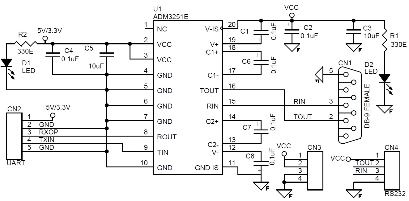
The charge pump voltage converter consists of a 200 kHz oscillator and a switching matrix. The converter generates a ±10.0 V supply from the input 5.0 V level. This is done in two stages by using a switched capacitor technique. First, the 5.0 V input supply is doubled to 10.0 V by using C6 as the charge storage element. The +10.0 V level is then inverted to generate −10.0 V using C7 as the storage element. Capacitor C2 and Capacitor C8 are used to reduce the output ripple. Their values are not critical and can be increased.
Schematic
Parts List
Connections
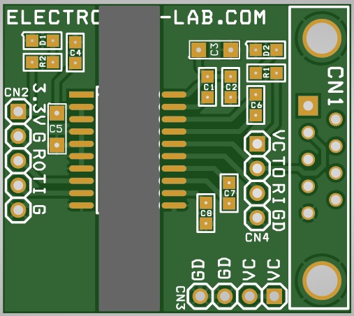
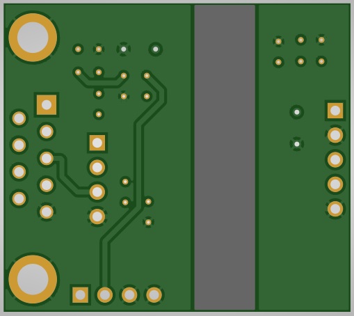
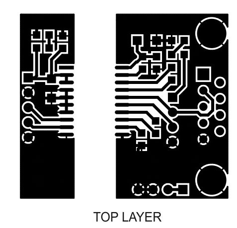
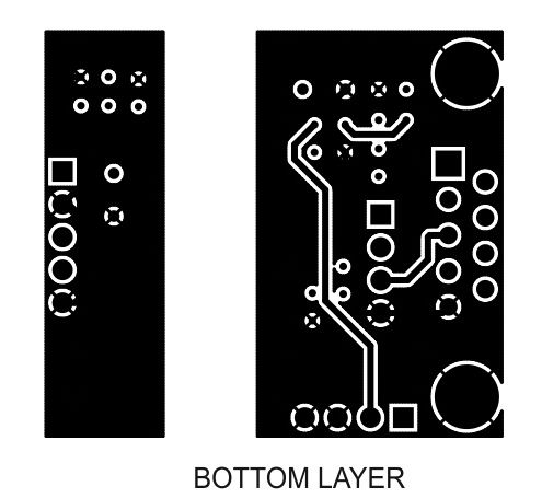
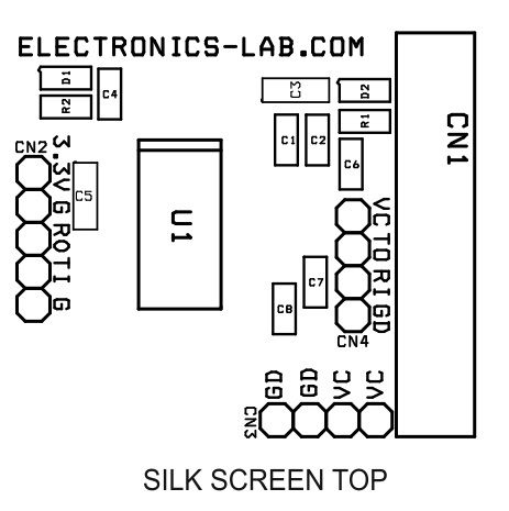
Gerber View





Hello,
In that video what value for VCC that you used?