
One Channel RF Remote Relay Switch
- Rajkumar Sharma
- 100 Views
- moderate
- Tested
- SKU: EL148385
- Quote Now
- 0 Likes

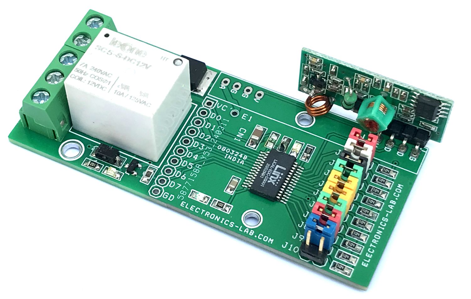
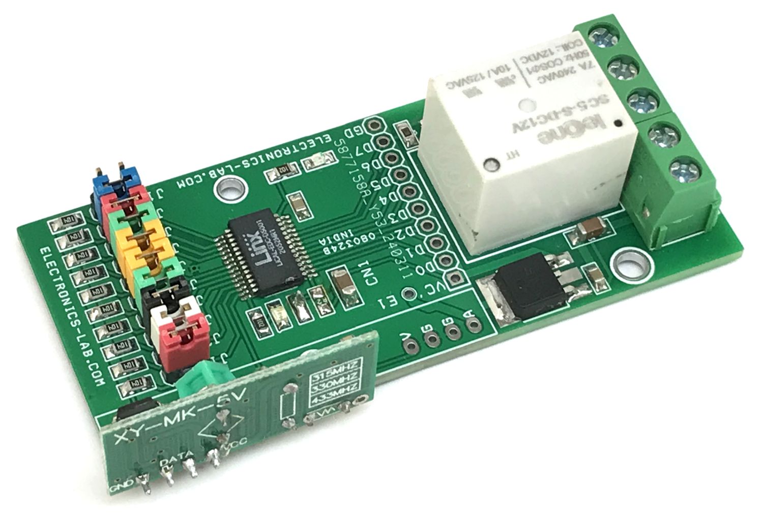
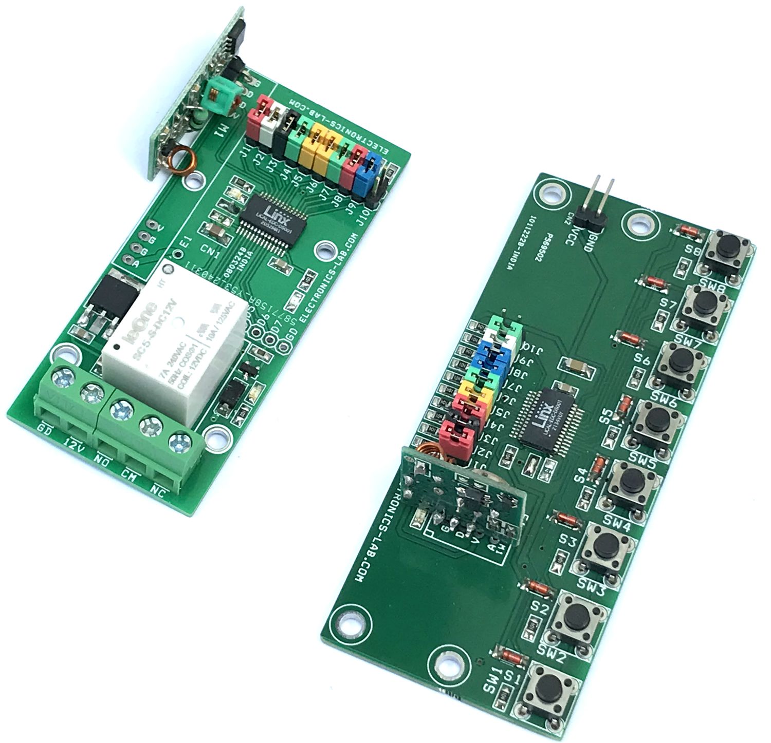
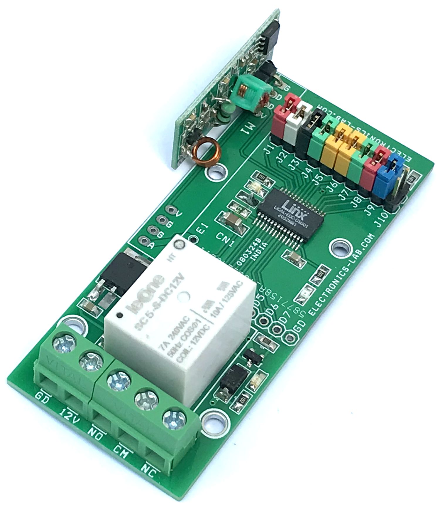
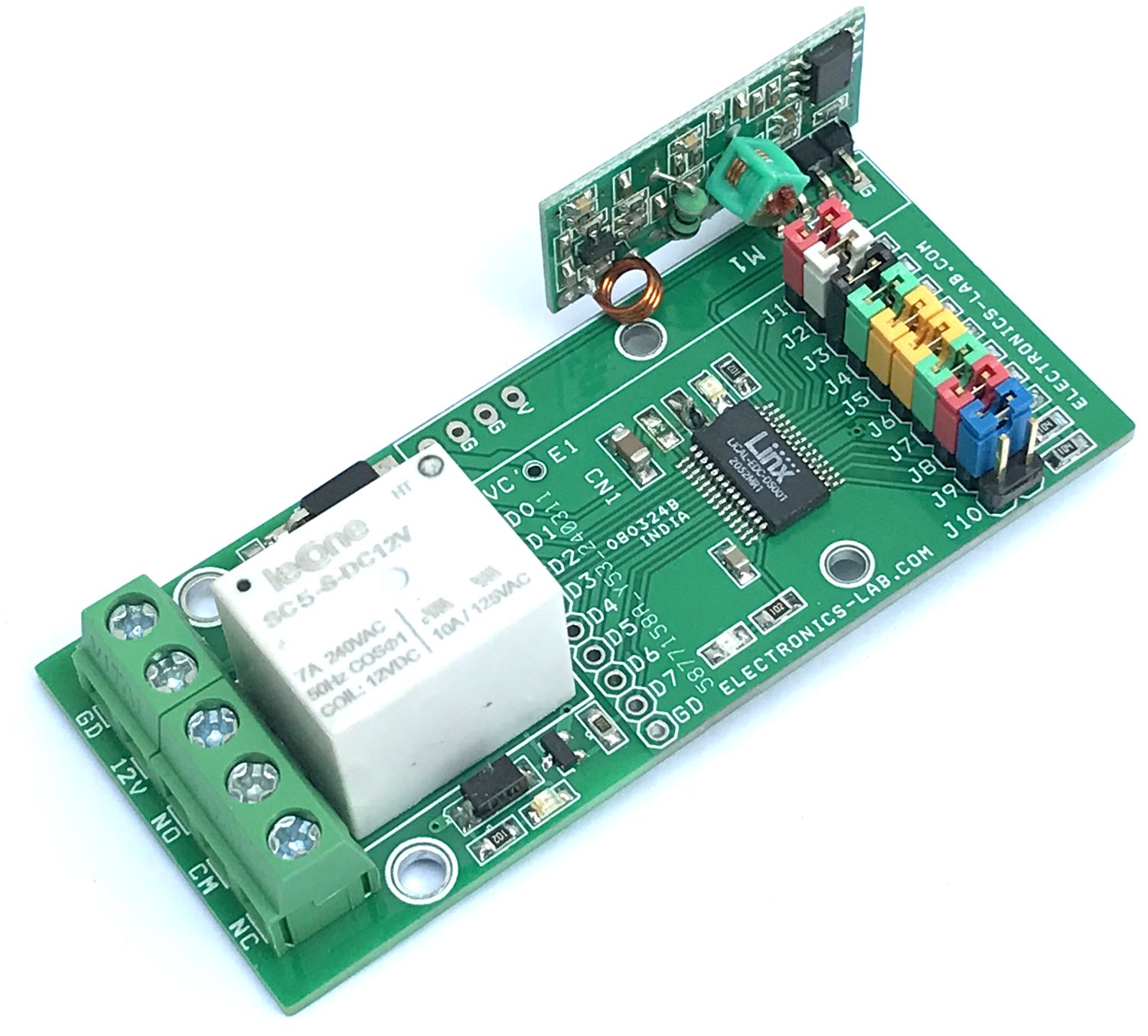
The project described here is one Channel RF remote receiver Relay board. The project is built using LICAL-EDC-DS001 chip from LINX. The board consists of Encoder/Decoder chip, 433Mhz RF Receiver module, 10 x jumpers to set the address, a Relay to drive the output, U2 5V regulator, header connector for data outputs for controlling external devices. All outputs are compatible with TTL logic, normally they are low and go high when a valid signal is received and decoded by the chip. D2 onboard Power LED, D1 LED indicates valid transmission signal. LED D4 shows the relay operations. The relay is connected to the D7 output. The rest D0 to D6 outputs are free and can be used to interface with another device using connector CN1. The relay board will act with D7-Switch 8 of the Remote Transmitter. The relay delivers momentary switching to a load up to 7A DC or AC. It can drive inductive, resistive, and capacitive loads such as Lamps, fans, solenoids, DC motors, AC motors etc.
Note: The receiver is compatible with the “8 Channel RF Remote Transmitter with Holtek and Serial Protocol” published on our website.
Features
- Supply 12V DC
- 10 Address Lines Selected through Jumpers J1 to J10
- Relay Connected to D7 Data Output
- On Board 5V Regulator
- 7 Data Output TTL Compatible Normally Low (Momentary)
- On Board Power LED
- On Board VT LED (Valid Transmission)
- ON Board Relay LED
- Relay Contacts Normally Open/Normally Closed
- Relay Contacts 7A/250V AC
- PCB Dimensions 45.09 x 33.02 mm
- 2 x 2.5 mm Mounting Holes
- 4 x 3 mm Mounting Holes
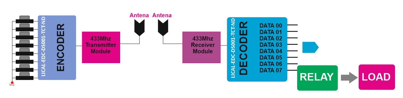
System Configuration
A simple remote-control system consists of an encoder, RF transmitter, RF receiver and a decoder. The encoder is connected to 8 buttons, The encoder detects the closure of one of the switches and converts that into a digital data stream. This data is then sent to an RF transmitter that conveys this data into free space. An RF receiver receives the data and sends it to a decoder. The decoder analyses the data and, if it is valid, replicates the switch closure on an output. This output is then connected to whatever circuitry is to be controlled. All outputs are momentary and TTL logic.
This DS series decoder and encoder chip is ideal for remote control applications. It decodes the signal received by 433 MHz RF modules. When the DS enters Decoder Mode, it checks the state of the DIN line. If it is high, the P_SEL line is checked to set which protocol is used and the decoder receives the data. It compares the address in the received packet to its local address lines. If they match, the data is stored and a second packet is received. With the Holtek® protocol, the decoder compares the two packets. If they match, the received data bits are output on the data lines and the VT line is pulled high thus LED D1 is on. This protocol compares each packet with the previous one looking for a match. The serial protocol requires two matching packets for initial activation and then updates the lines on each subsequent packet. The DS then looks for the next packet on the DIN line. With the Holtek® protocol, once no valid data is received (there is a mismatch of address, data, or bit timings), the Data and VT lines are pulled low and the DS goes to sleep until DIN is pulled high. The Serial protocol holds the output states until a 130ms timer runs out. The Holtek® protocol compares two packets and, if they match, sets the outputs. If a data line is toggled during a transmission (D1 is activated while D0 is already active) then the received packet does not match the previous packet and the output lines are pulled low until the next packet arrives. This causes all of the outputs to briefly cut out when a line is toggled. The serial protocol uses a timer to prevent this cutout.
LICAL-EDC-DS001 Encoder/Decoder Chip
The same part can be used as encoder or decoder by selecting state of one pin. The DS Series also has two protocols built into the same part, selected by the state of a single pin. One is compatible with Holtek devices, such as the HT640 and HT658. The other protocol is a serial data structure that is much more immune to noise and edge jitter. This protocol offers much more range and reliability than the Holtek protocol while keeping the simple jumper-addressing.
Theory of Operation
The DS Series is a remote-control encoder and decoder that offers two protocols in one part based on the state of the P_SEL line. The first protocol operates with the Holtek® HT640 encoder and HT658 decoder. The second is a serial protocol that offers more noise immunity and faster response time while keeping the simple addressing. The DS can operate as either an encoder or decoder based on the state of the E/D_SEL line. It does not operate as both simultaneously. When set as an encoder it monitors the state of the TE line. When the line is high the DS records the states of the data and address lines, assembles them into a packet and outputs the packet three times. The data lines can be connected to switches or contacts. The address lines can be set with Jumpers. When set as a decoder the DS receives packets and validates them. The validation includes checking the bit timings and comparing the received address to the local address line settings. Two matching packets must be received consecutively. If the timings are good and the addresses match, the DS sets its data lines to match the received states. These lines can be connected to the application circuitry to be controlled. When the TE/DIN line is low, the DS goes into a low power sleep mode.
Setting the Address
The project has ten address lines. This allows the formation of up to 1,022 (210 – 2) unique transmitter-receiver relationships, Jumper J1 to J10 can be used to set the address, all lines are pulled high. The chip rejects packets with addresses set to all high or all low. At least one address line must be different from the rest. The encoder does transmit all addresses, but the decoder rejects packets with all address lines set the same. The receiver’s address line states must match the transmitter’s exactly for a transmission to be recognized. If the addresses do not match, then the decoder takes no action.
Initial Operation
On power-up, the E/D_SEL line is tested to determine if the DS operates as an encoder or a decoder. If the line is high, the DS enters Encoder Mode. If low, it enters Decoder Mode. This is checked once on power-up. Once the operating mode is selected, the data-line direction is set. In either mode a rising edge on the TE/DIN line wakes the device from low-power sleep.
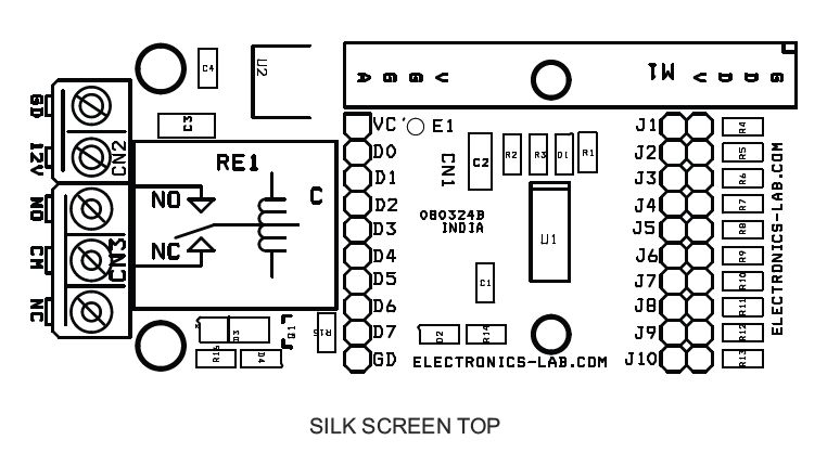
Connections and Other Information
- Connections and Other Details
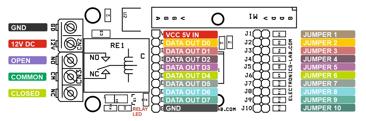
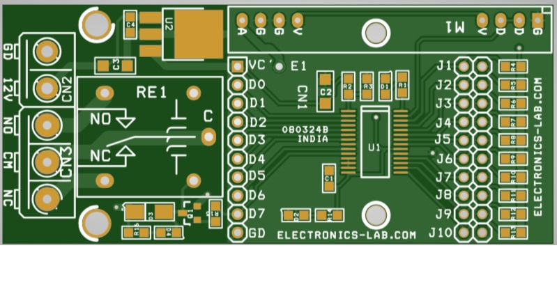
- CN1: Pin 1 = VCC 5V In, Pin 2 = D0, Pin 3 = D1, Pin 4 = D2, Pin 5 = D3, Pin 6 = D4, Pin 7 = D5, Pin 8 = D6, Pin 9 = D7, Pin 10 GND
- D1: Valid Signal LED
- D2: Power LED
- Jumper: J1 to J10 for Address Configuration
- For Serial Protocol R2 = 0 Ohms, R3 Omit, For Holtek Protocol R3= 0 Ohms and R2 Omit (Read Datasheet of chip for Serial/Holtek Protocol)
- CN2: Pin 1 = 12V DC, Pin 2 GND
- CN3: Relay Contacts Pin1 – Normally Closed, Pin 2 Common, Pin 3 = Normally Open
Schematic
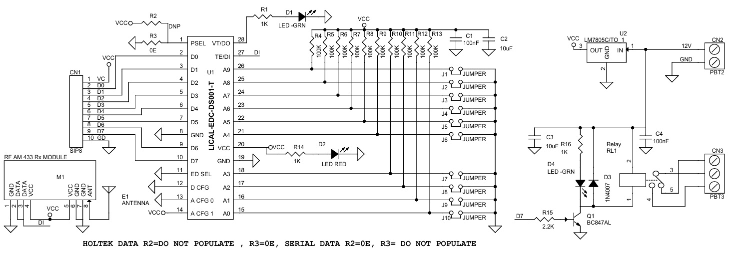
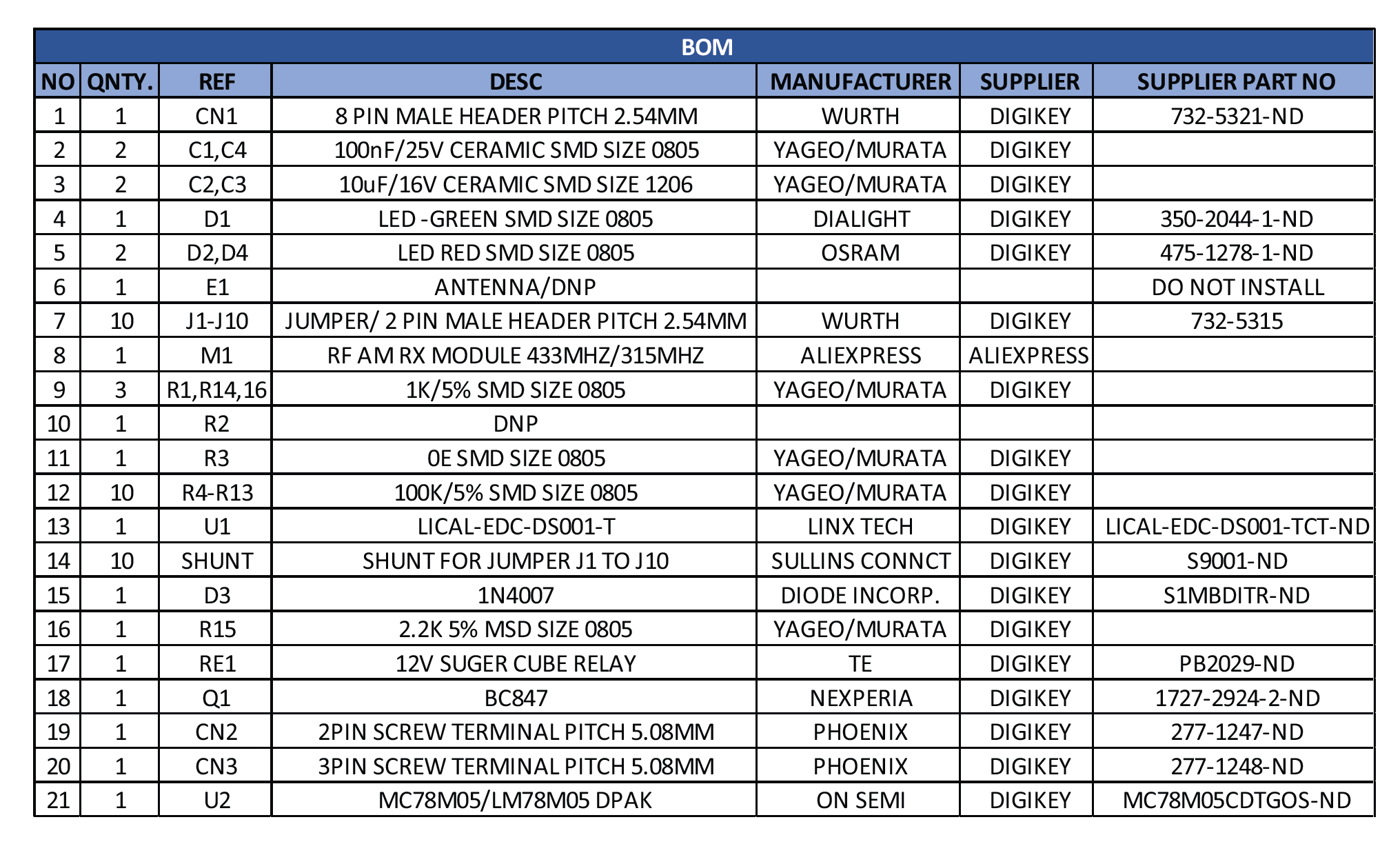
Parts List
| NO | QNTY. | REF | DESC | MANUFACTURER | SUPPLIER | SUPPLIER PART NO |
|---|---|---|---|---|---|---|
| 1 | 1 | CN1 | 8 PIN MALE HEADER PITCH 2.54MM | WURTH | DIGIKEY | 732-5321-ND |
| 2 | 2 | C1,C4 | 100nF/25V CERAMIC SMD SIZE 0805 | YAGEO/MURATA | DIGIKEY | |
| 3 | 2 | C2,C3 | 10uF/16V CERAMIC SMD SIZE 1206 | YAGEO/MURATA | DIGIKEY | |
| 4 | 1 | D1 | LED -GREEN SMD SIZE 0805 | DIALIGHT | DIGIKEY | 350-2044-1-ND |
| 5 | 2 | D2,D4 | LED RED SMD SIZE 0805 | OSRAM | DIGIKEY | 475-1278-1-ND |
| 6 | 1 | E1 | ANTENNA/DNP | DO NOT INSTALL | ||
| 7 | 10 | J1-J10 | JUMPER/ 2 PIN MALE HEADER PITCH 2.54MM | WURTH | DIGIKEY | 732-5315 |
| 8 | 1 | M1 | RF AM RX MODULE 433MHZ/315MHZ | ALIEXPRESS | ALIEXPRESS | |
| 9 | 3 | R1,R14,16 | 1K/5% SMD SIZE 0805 | YAGEO/MURATA | DIGIKEY | |
| 10 | 1 | R2 | DNP | |||
| 11 | 1 | R3 | 0E SMD SIZE 0805 | YAGEO/MURATA | DIGIKEY | |
| 12 | 10 | R4-R13 | 100K/5% SMD SIZE 0805 | YAGEO/MURATA | DIGIKEY | |
| 13 | 1 | U1 | LICAL-EDC-DS001-T | LINX TECH | DIGIKEY | LICAL-EDC-DS001-TCT-ND |
| 14 | 10 | SHUNT | SHUNT FOR JUMPER J1 TO J10 | SULLINS CONNCT | DIGIKEY | S9001-ND |
| 15 | 1 | D3 | 1N4007 | DIODE INCORP. | DIGIKEY | S1MBDITR-ND |
| 16 | 1 | R15 | 2.2K 5% MSD SIZE 0805 | YAGEO/MURATA | DIGIKEY | |
| 17 | 1 | RE1 | 12V SUGER CUBE RELAY | TE | DIGIKEY | PB2029-ND |
| 18 | 1 | Q1 | BC847 | NEXPERIA | DIGIKEY | 1727-2924-2-ND |
| 19 | 1 | CN2 | 2PIN SCREW TERMINAL PITCH 5.08MM | PHOENIX | DIGIKEY | 277-1247-ND |
| 20 | 1 | CN3 | 3PIN SCREW TERMINAL PITCH 5.08MM | PHOENIX | DIGIKEY | 277-1248-ND |
| 21 | 1 | U2 | MC78M05/LM78M05 DPAK | ON SEMI | DIGIKEY | MC78M05CDTGOS-ND |
Connections
System Diagram
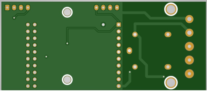
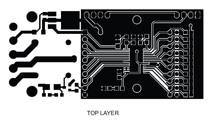
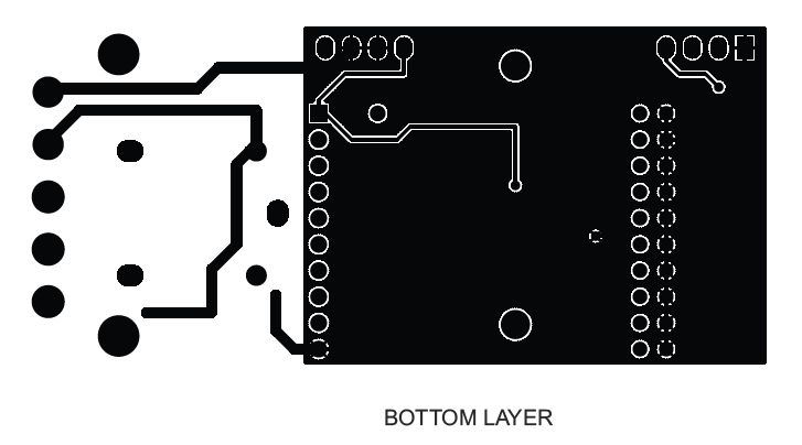
Gerber View
Photos
Video
LICAL-EDC-DS001-T Datasheet
Please follow and like us:
PCB


Subscribe
Login
0 Comments