

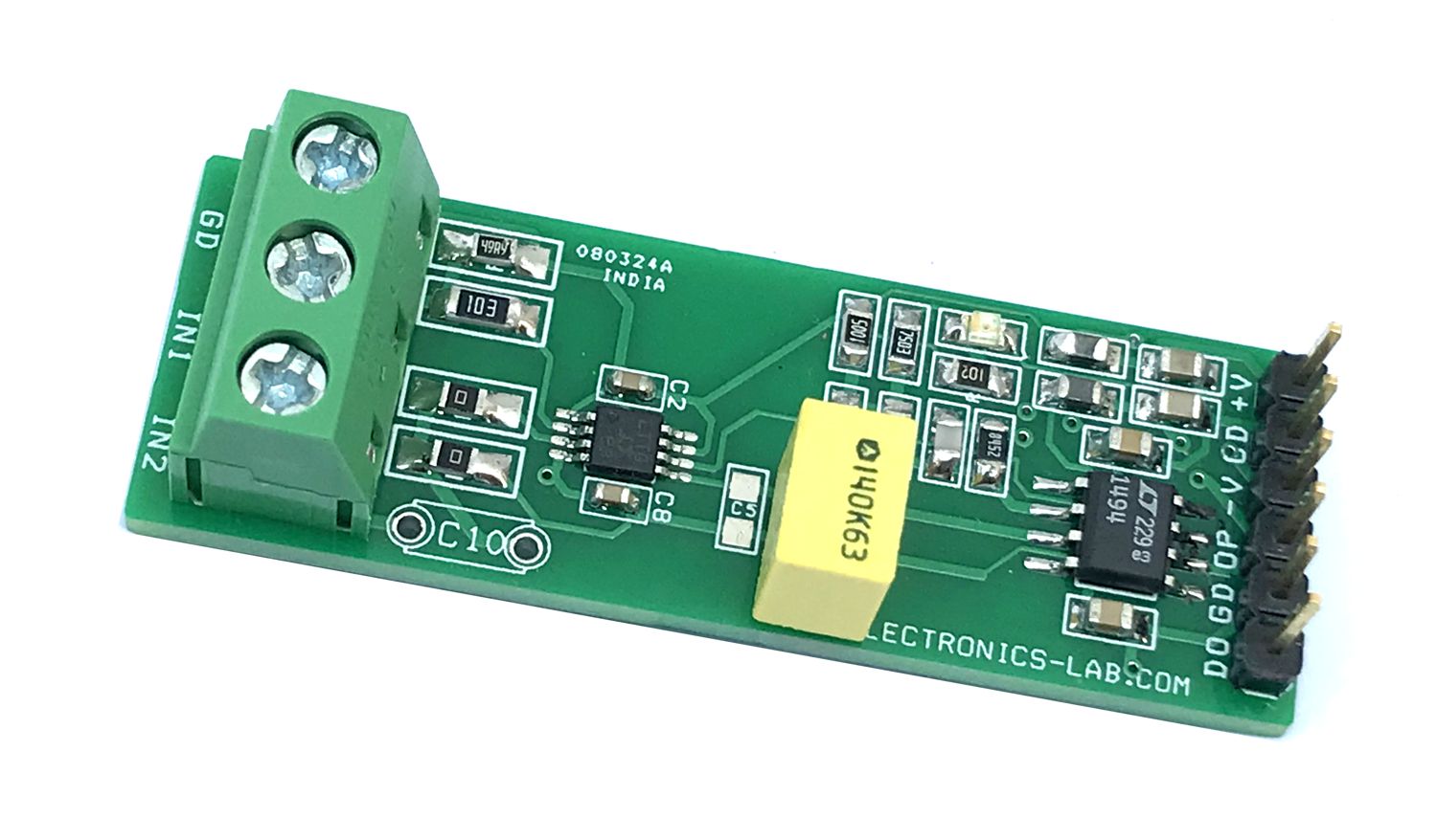
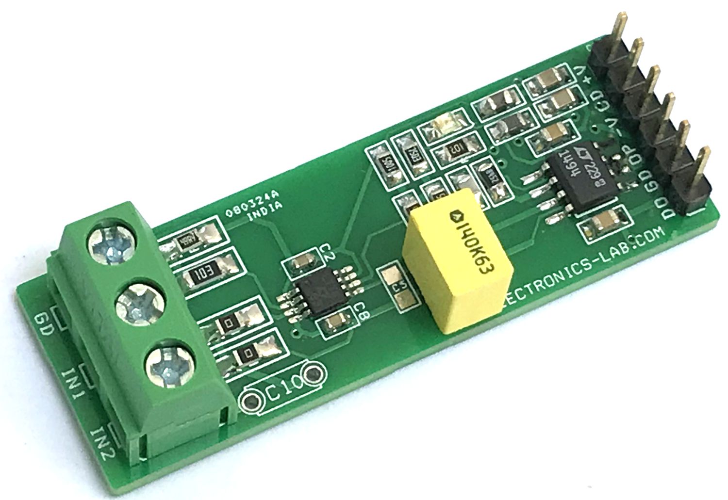
RMS To DC Converter
- Rajkumar Sharma
- 203 Views
- moderate
- Tested
- SKU: EL148445
- Quote Now
- 0 Likes

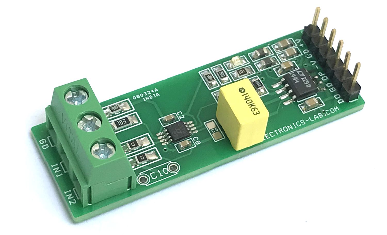
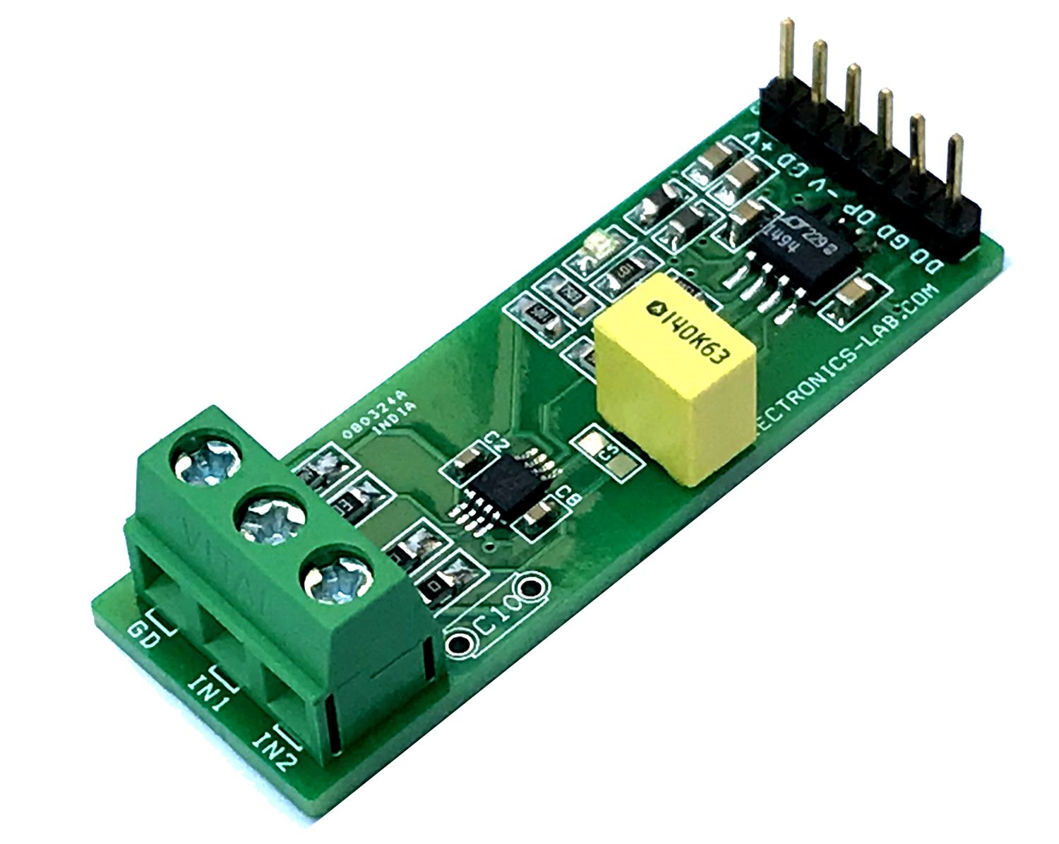
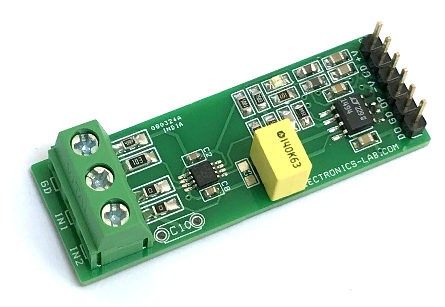
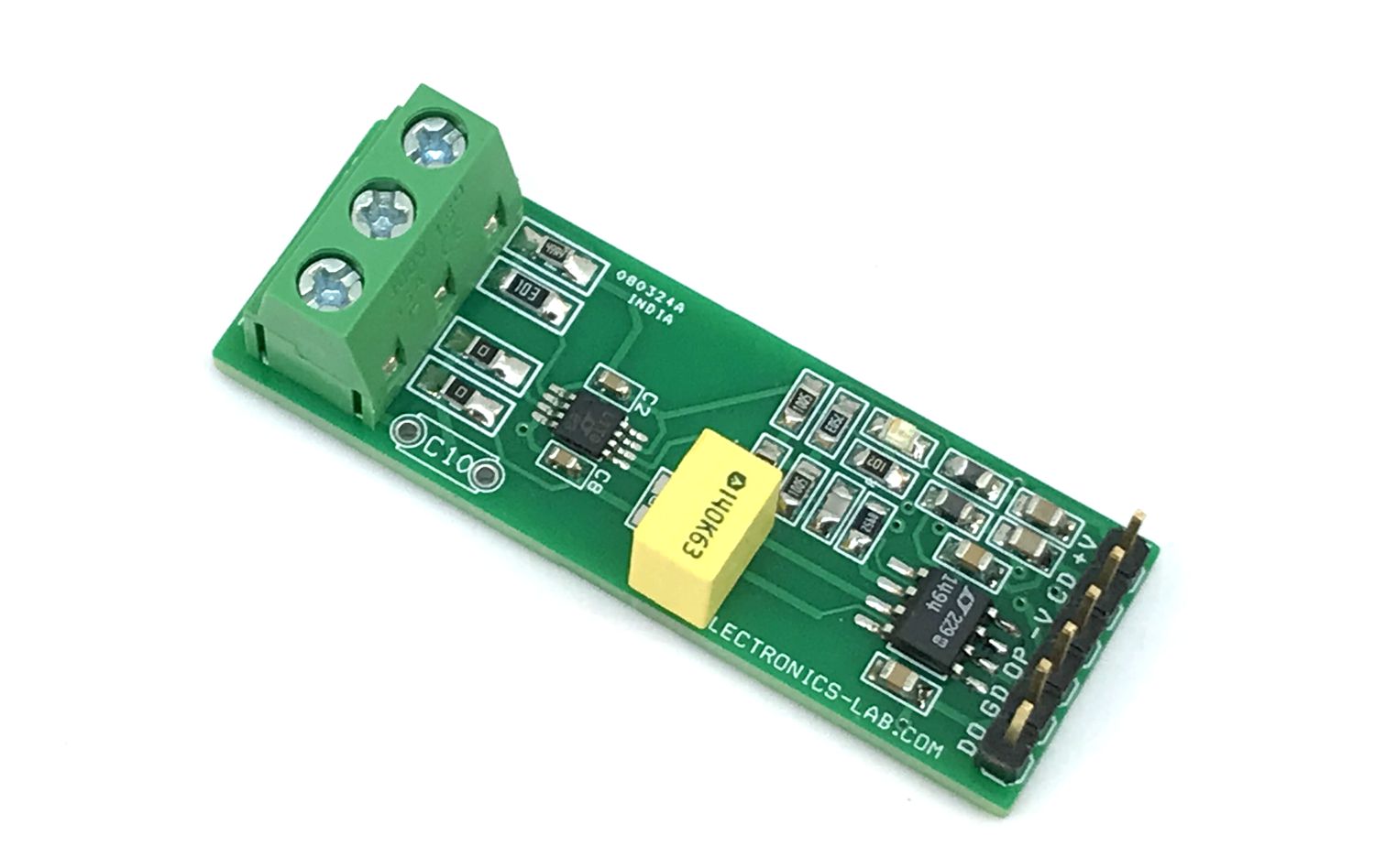
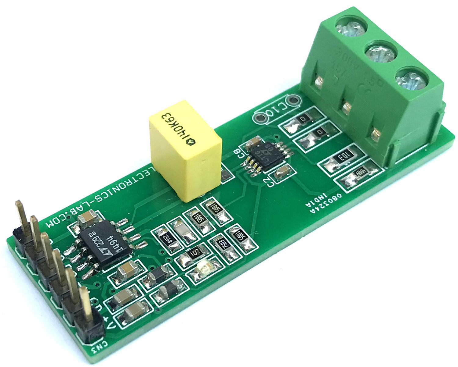
This is a Precision Micro-power true RMS-to-DC converter built using LTC1966 RMS to DC Converter chip and op-amp LTC1494. The RMS to DC that is Converted by LTC1966 and op-amp is used as a post filter to improve AC Response with Offset and Gain Correction. The circuit converts the AC signal into DC. The project works with a single AC input signal and a variety of passive components provided to support configurations for varied applications. Input 1 and Input 2 can be used to feed differential signals. In this case choose appropriate components as per application requirement. Please refer to the datasheet of LTC1966 for more information. The board operates with a dual power supply +/-5V DC. The input voltage range is up to 1V and the output is also up to 1V.
Features
- Power Supply ±5.5V (Dual Supply)
- True RMS DC Conversion Using ∆Σ Technology
- High Accuracy: 0.1% Gain Accuracy from 50Hz to 1kHz, 0.25% Total Error from 50Hz to 1kHz
- High Linearity: 0.02% Linearity Allows Simple System Calibration
- Constant Bandwidth: Independent of Input Voltage 800kHz –3dB, 6kHz ±1%
- Flexible Inputs: Differential or Single-Ended
- Up to 1VPEAK Differential Voltage
- Output 0 to 1V
- Flexible Output: Rail-to-Rail Output
- PCB Dimensions 50.80 x 17.78 mm
Applications
- True RMS Digital Multi Meters
- True RMS Panel Meters
- True RMS AC + DC Measurements
- Electricity Meters
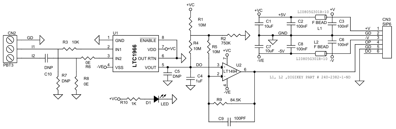
The LTC1966 is a true RMS-to-DC converter that utilizes an innovative patented ∆Σ computational technique. The internal delta sigma circuitry of the LTC1966 makes it simpler to use, more accurate, lower power and dramatically more flexible than conventional log antilog RMS-to-DC converters. The LTC1966 accepts single-ended or differential input signals (for EMI/RFI rejection) and supports crest factors up to 4. Common mode input range is rail-to-rail. Differential input range is 1VPEAK, and offers unprecedented linearity. Unlike previously available RMS-to-DC converters, the superior linearity of the LTC1966 allows hassle free system calibration at any input voltage. The LTC1966 also has a rail-to-rail output with a separate output reference pin providing flexible level shifting. The LTC1966 operates on a single power supply from 2.7V to 5.5V or dual supplies up to ±5.5V. A low power shutdown mode reduces supply current to 0.5μA.
Circuit shows an analog implementation of this with the offset and gain errors corrected; only the slight, but necessary, degradation in nonlinearity remains. The circuit works by creating approximately 300mV of bias at the junction of the 10MΩ resistors when the LTC1966’s input/output are zero. The 10MΩ resistor to the LTC1966 output therefore feeds in 30nA. The loading of this resistor causes a slight reduction in gain which is corrected, as is the nominal 2.5mV offset, by the LT1494 op amp. The two 10MΩ resistors not connected to the supply can be any value as long as they match and the feed voltage is changed for 30nA injection. The op amp gain is only 1.00845, so the output is dominated by the LTC1966 RMS results, which keeps errors low. With the values shown, the 84.5k resistor is the closest match in the 1% EIA values. This low error sensitivity is important because the LTC1966 output impedance is 85kΩ ±11.8%, which can create a gain error of ±0.1%; enough to degrade the overall gain accuracy somewhat. This gain variation term is increased with lower value feed resistors, and decreased with higher value feed resistors. A bigger error caused by the variation of the LTC1966 output impedance is imperfect cancelation of the output offset introduced by the injected current. The offset correction provided by the LT1494 will be based on a consistent 84.5kΩ times the injected current, while the LTC1966 output impedance will vary enough that the output offset will have a ±300µV range about the nominal 2.5mV. If the two 10MΩ feed resistors to the LT1494 have significant mismatch, cancellation of the 2.5mV offset would be further impacted, so it is probably worth paying an extra penny or so for 1% resistors or even the better temperature stability of thin film devices. The 300mV feed voltage is not particularly critical because it is nominally cancelled, but the offset errors due to these resistance mismatches is scaled by that voltage. Note that the input bias current of the op amp used in circuit is also nominally cancelled, but it will add or subtract to the total current injected into the LTC1966 output. With the 1nA IBIAS of the LT1494 this is negligible. While it is possible to eliminate the feed resistors by using an op amp with a PNP input stage whose IBIAS is 30nA this circuit needs a minimum of 30nA, therefore such an approach may not always work. Because the circuit subtracts the offset created by the injected current, the LT1494 output with zero LTC1966 input will rest at +2.5mV, nominal before offsets, rather than the 5mV.
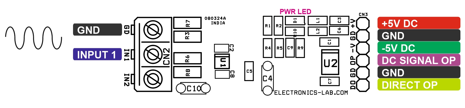
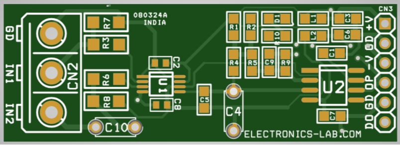
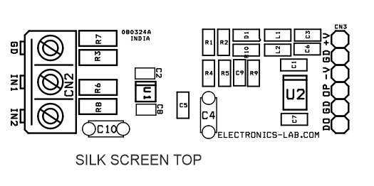
Connections
- CN2: Pin1 = GND, Pin 2 = AC Signal Input, Pin 3 = Optional Input 2
- CN3: Pin 1 = +V 5V, Pin 2 = GND, Pin 3 = -5V, Pin 4 = DC Signal Output, Pin 5 = GND, Pin 6 = Direct Output from LTC1966
- D1: Power LED
Schematic
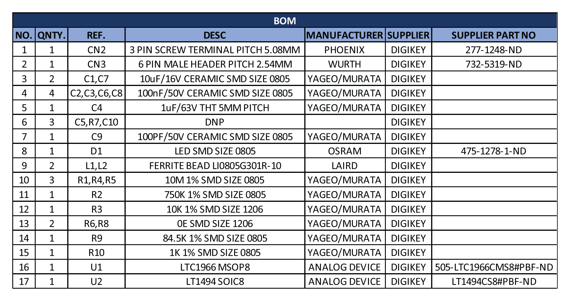
Parts List
| NO. | QNTY. | REF. | DESC | MANUFACTURER | SUPPLIER | SUPPLIER PART NO |
|---|---|---|---|---|---|---|
| 1 | 1 | CN2 | 3 PIN SCREW TERMINAL PITCH 5.08MM | PHOENIX | DIGIKEY | 277-1248-ND |
| 2 | 1 | CN3 | 6 PIN MALE HEADER PITCH 2.54MM | WURTH | DIGIKEY | 732-5319-ND |
| 3 | 2 | C1,C7 | 10uF/16V CERAMIC SMD SIZE 0805 | YAGEO/MURATA | DIGIKEY | |
| 4 | 4 | C2,C3,C6,C8 | 100nF/50V CERAMIC SMD SIZE 0805 | YAGEO/MURATA | DIGIKEY | |
| 5 | 1 | C4 | 1uF/63V THT 5MM PITCH | YAGEO/MURATA | DIGIKEY | |
| 6 | 3 | C5,R7,C10 | DNP | DIGIKEY | ||
| 7 | 1 | C9 | 100PF/50V CERAMIC SMD SIZE 0805 | YAGEO/MURATA | DIGIKEY | |
| 8 | 1 | D1 | LED SMD SIZE 0805 | OSRAM | DIGIKEY | 475-1278-1-ND |
| 9 | 2 | L1,L2 | FERRITE BEAD LI0805G301R-10 | LAIRD | DIGIKEY | |
| 10 | 3 | R1,R4,R5 | 10M 1% SMD SIZE 0805 | YAGEO/MURATA | DIGIKEY | |
| 11 | 1 | R2 | 750K 1% SMD SIZE 0805 | YAGEO/MURATA | DIGIKEY | |
| 12 | 1 | R3 | 10K 1% SMD SIZE 1206 | YAGEO/MURATA | DIGIKEY | |
| 13 | 2 | R6,R8 | 0E SMD SIZE 1206 | YAGEO/MURATA | DIGIKEY | |
| 14 | 1 | R9 | 84.5K 1% SMD SIZE 0805 | YAGEO/MURATA | DIGIKEY | |
| 15 | 1 | R10 | 1K 1% SMD SIZE 0805 | YAGEO/MURATA | DIGIKEY | |
| 16 | 1 | U1 | LTC1966 MSOP8 | ANALOG DEVICE | DIGIKEY | 505-LTC1966CMS8#PBF-ND |
| 17 | 1 | U2 | LT1494 SOIC8 | ANALOG DEVICE | DIGIKEY | LT1494CS8#PBF-ND |
Connections
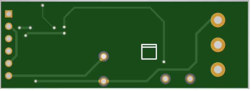
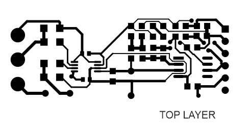
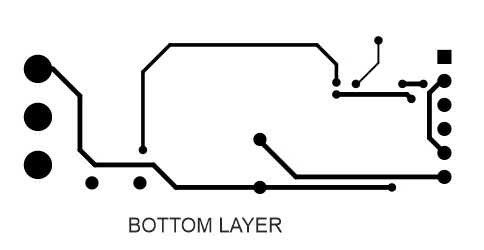
Gerber View
Photos
Video
LTC1966 Datasheet
Please follow and like us:
PCB


Subscribe
Login
0 Comments


")

