Video Driver with Built-in 6 Channel Input Selection Switch
- Rajkumar Sharma
- 296 Views
- easy
- Tested
- SKU: EL136311
- Quote Now
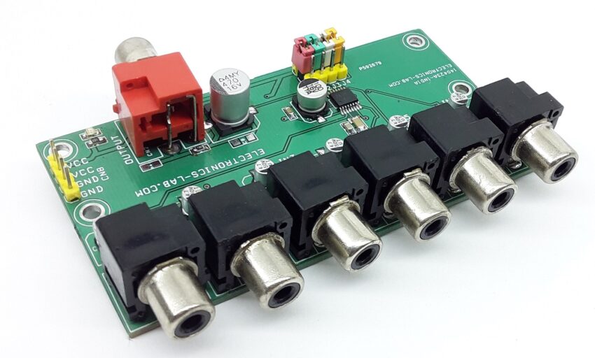
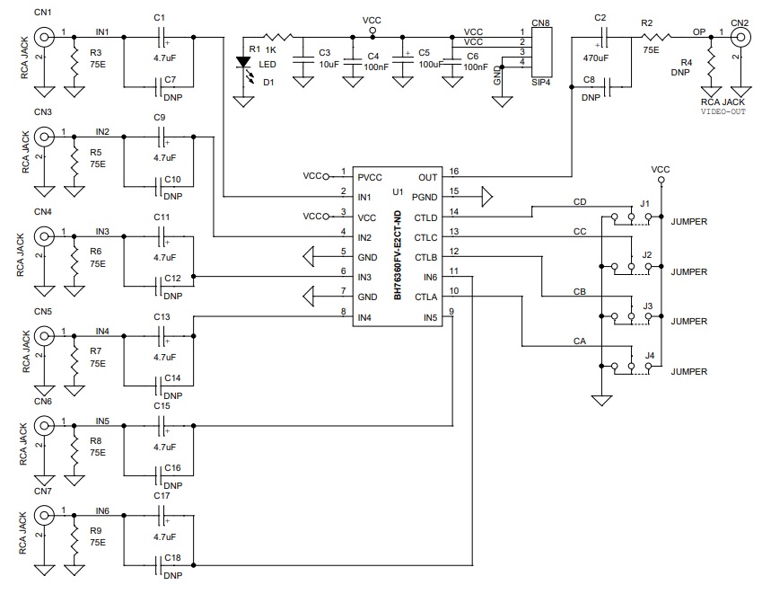
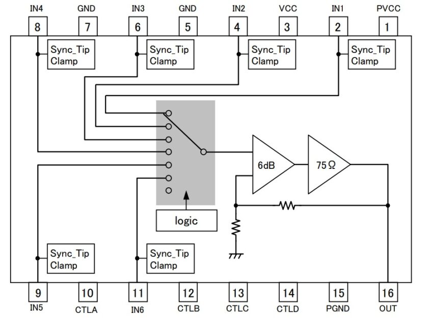
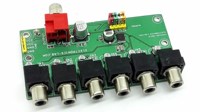
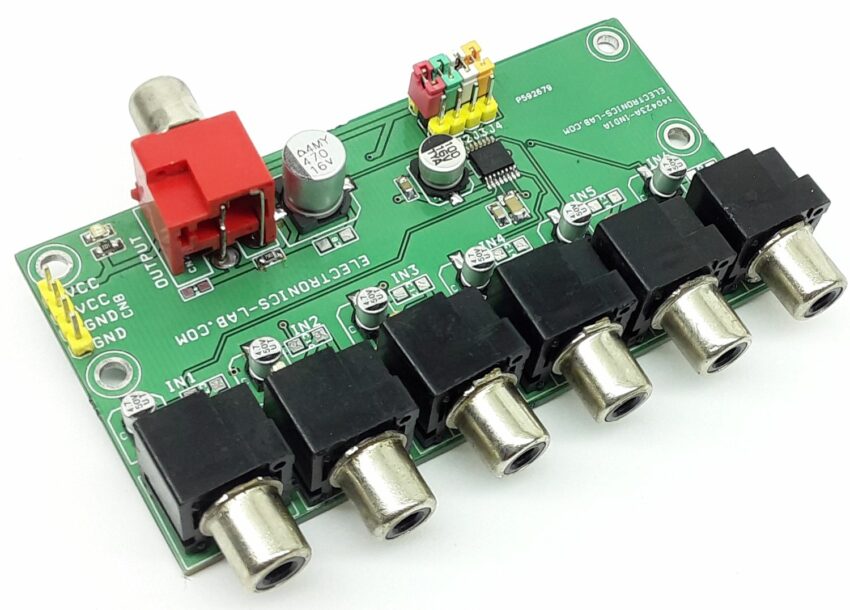
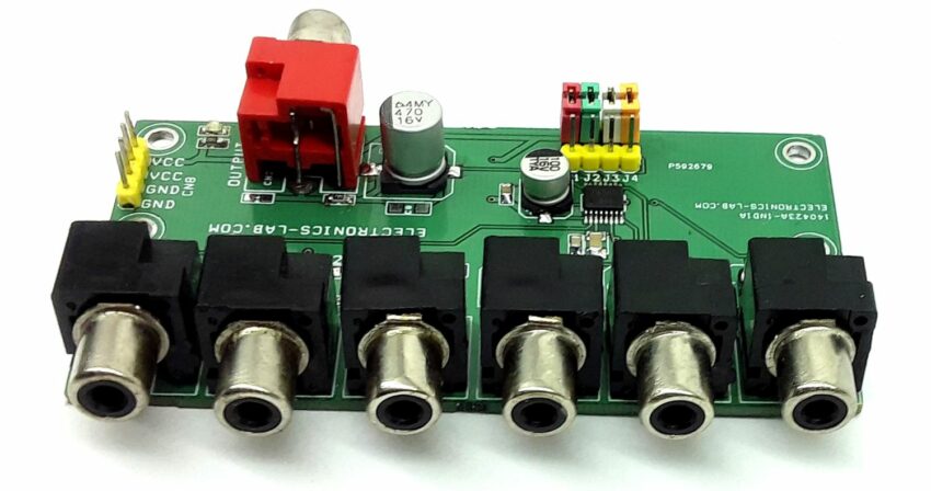
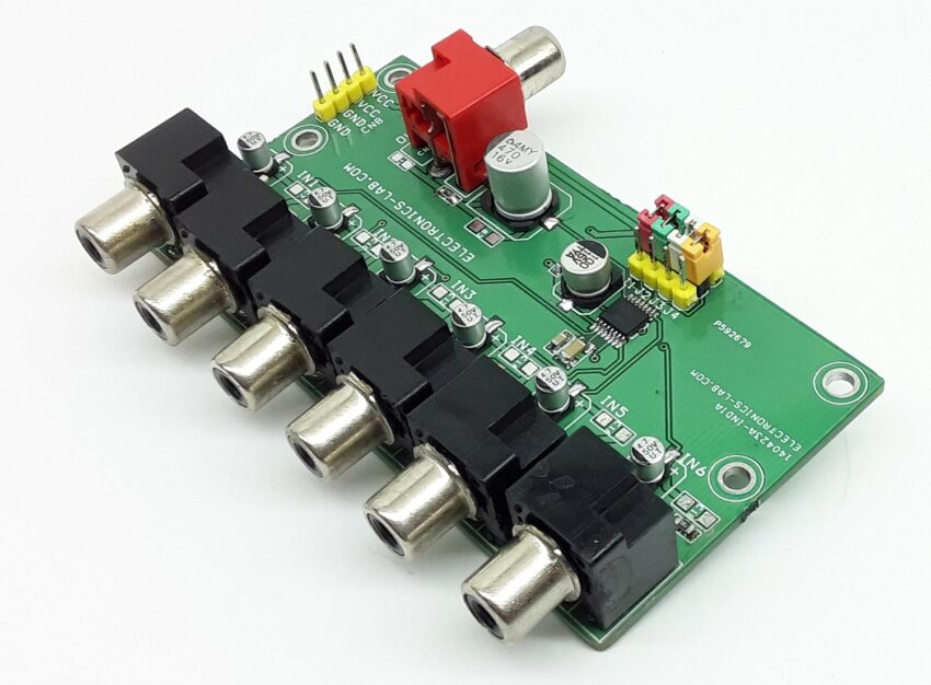
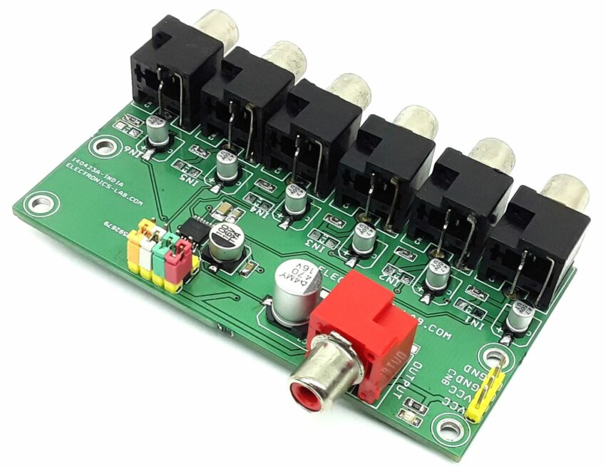
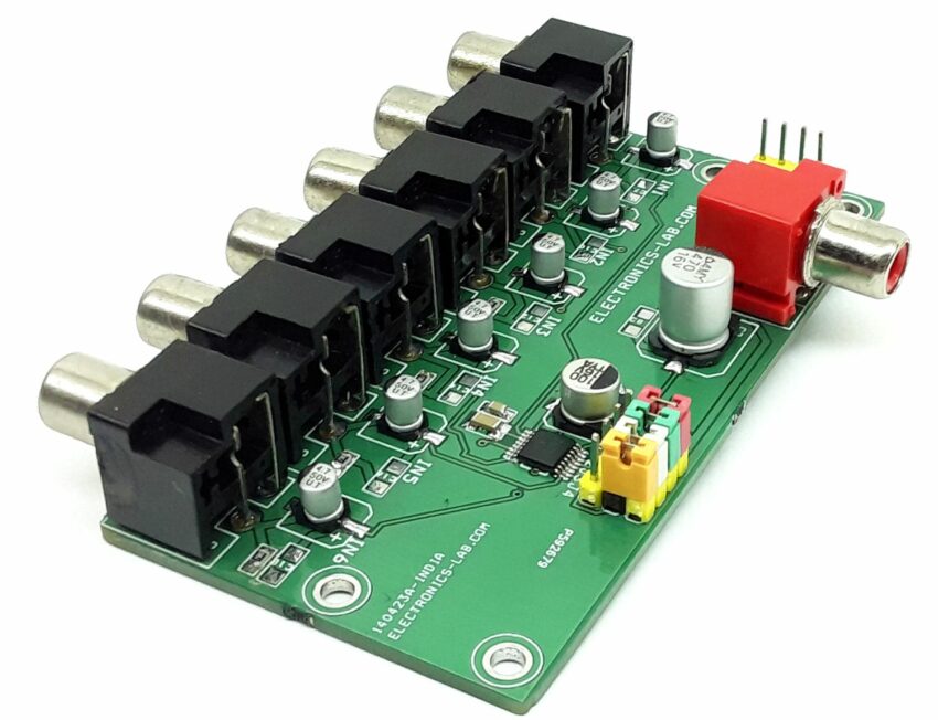
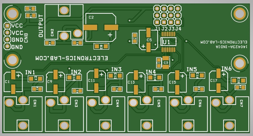
The project presented here is a video driver with 6 channel input selection using onboard jumpers or a microcontroller interface. The circuit features a wide dynamic range and frequency response. The IC can be used with low voltage starting at VCC=2.8V and the project supports a broad range of input signals, depending on whether or not a 6-dB video and video driver is included and what combination of sync tip clamp type and bias (resistor terminal) type input is used. RCA connectors are provided for video input and output connection. The header connector helps to power the board. Jumpers J2 to J3 are provided to select the input channels. 6-channel video selection can also be controlled using an external circuit or microcontroller by applying high or low TTL signal to CTLA, CTLB, CTLC, CTLD pins. In this case, use the center pins of jumper J1 to J4.
Features
- Power supply voltage, from 2.8 V to 5.5 V
- Wide output dynamic range
- Excellent frequency response 100kHz/10MHz 0dB[Typ.]
- No crosstalk between channels (Typ. -65 dB, f = 4.43 MHz)
- Built-in standby function, circuit current during standby is 0 µA (Typ.)
- Sync tip clamp input
- Video Amplifier Gain 6dB
- 6-dB amp and 75Ohms driver are built-in
- Maximum Output Level 3.8Vpp (f=10Khz, THD=1%)
- Input Voltage Range o to VCC+0.2V
- Control Pin Switch Level 1.2V Minimum High Level, 0.45V Maximum Low-Level Threshold Voltage
- Input Impedance 150K Ohms
- PCB Dimensions 91.44 x 48.10mm
- 4 x 3mm Mounting Holes
Connections and Other Details
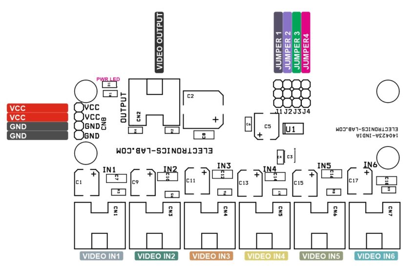
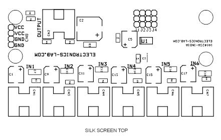
- CN1: RCA Female = Video Input 1
- CN3: RCA Female = Video Input 2
- CN4: RCA Female = Video Input 3
- CN5: RCA Female = Video Input 4
- CN6: RCA Female = Video Input 5
- CN7: RCA Female = Video Input 6
- CN2: RCA Female = Video Output
- CN8: Pin 1, 2 = VCC, Pin 3, 4 = GND
- Jumper J1: Control D
- Jumper J2: Control C
- Jumper J3: Control B
- Jumper J4: Control A
- D1: Power LED
Input Selection Jumper J1 – J4
- IN1 = J1=H, J2=L, J3=L, J4=L
- IN2 = J1=H, J2=L, J3=L, J4=H
- IN3 = J1=H, J2=L, J3=H, J4=L
- IN4 = J1=H, J2=L, J3=H, J4=H
- IN5 = J1=H, J2=H, J3=L, J4=L
- IN6 = J1=H, J2=H, J3=L, J4=H
- Mute = J1=H, J2=H , J3=H, J4=X
- STBY = J1=Open/L , J2=X, J2=X, J4=X
- X= L(Open)Or H Either Is Possible
Schematic
IC Block Diagram
Parts List
| NO. | QNTY. | REF | DESC. | MANUFACTURER | SUPPLIER | SUPPLIER'S PART |
|---|---|---|---|---|---|---|
| 1 | 7 | CN1,CN2,CN3,CN4,CN5,CN6,CN7 | RCA JACK | KEYSTONE | DIGIKEY | 36-973-ND |
| 2 | 1 | CN8 | SIP4 | WURTH | DIGIKEY | 732-5317-ND |
| 3 | 6 | C1,C9,C11,C13,C15,C17 | 4.7uF/50V ELECTROLYTIC 5.30 X 6.50MM | KEMET | DIGIKEY | 399-6687-2-ND |
| 4 | 1 | C2 | 470uF/25V | RUBYCON | DIGIKEY | 1189-1588-2-ND |
| 5 | 1 | C3 | 10uF/25V Ceramic SMD SIZE 1210 or 1206 | YAGEO/MURATA | DIGIKEY | |
| 6 | 2 | C4,C6 | 100nF/50V CERAMIC SMD SIZE 0805 | YAGEO/MURATA | DIGIKEY | |
| 7 | 1 | C5 | 100uF/16V OR 25V ELECTROLYTIC | NICHICON | DIGIKEY | 493-9418-2-ND |
| 8 | 8 | R4,C7,C8,C10,C12,C14,C16,C18 | DNP | DIGIKEY | ||
| 9 | 1 | D1 | LED RED SMD SIZE 0805 | LITE ON INC | DIGIKEY | 160-1427-1-ND |
| 10 | 4 | J1,J2,J3,J4 | 2 PIN MALE HEADER PITCH 2.54MM | WURTH | DIGIKEY | 732-5315-ND |
| 11 | 1 | R1 | 1K 5% SMD SIZE 0805 | YAGEO/MURATA | DIGIKEY | |
| 12 | 7 | R2,R3,R5,R6,R7,R8,R9 | 75E 1% SMD SIZE 0805 | YAGEO/MURATA | DIGIKEY | |
| 13 | 1 | U1 | BH76360FV-E2CT-ND | ROHM | DIGIKEY | BH76360FV-E2CT-ND |
| 14 | 4 | SHUNT FOR JUMPER | JUMPER SHUNT FOR J1,J2,J3,J4 | SULINS CONCT | DIGIKEY | S9001-ND |
Connections