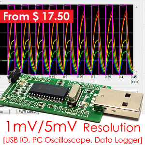


Tag: 3D-TSV

Technology
Samsung unveils 12-layer 3D-TSV chip packaging technology
An industry’s first, the 12-layer 3D-TSV (Through Silicon Via) technology developed by Samsung Electronics enables the stacking of 12 DRAM chips using more than 60,000 TSV holes, while maintaining the same thickness as current 8-layer chips. By Julien Happich @...
Continue Reading