Tag: wafer
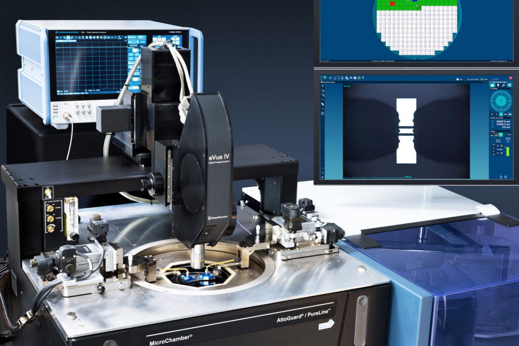
Rohde & Schwarz announces on-wafer device characterization test solution
Rohde & Schwarz now offers a test solution for full RF performance characterization of the DUT on-wafer which combines the powerful R&S ZNA vector network analyzer from Rohde & Schwarz with industry-leading engineering probe systems from FormFactor. As a result,...
Continue Reading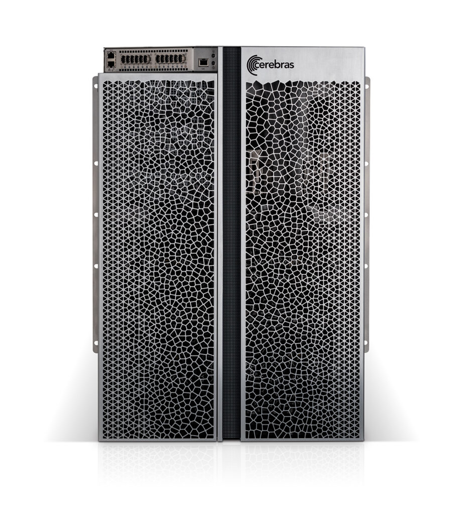
Cerebra establishes a new benchmark for training largest AI models on a single processor
Cerebras Systems recently announced a milestone of training multibillion-parameter Natural Language Processing (NLP) models, including GPT-3XL 1.3 billion models, GPT-J 6B, GPT-3 13B, and GPT-NeoX 20B, on a single CS-2 system. According to the claims made by Cerebras Systems, a single...
Continue Reading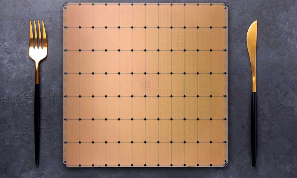
Cererbras’ All NEW Wafer Scale Engine Packs 2.6 Trillion Transistors For Deep Learning Workloads
In 2019, we saw one of the largest single computer chips manufactured by a California-based AI startup, Cerebras, that unveiled the Wafer-Scale Engine for deep learning applications. The 1.2 trillion transistors-packed Wafer-Scale Engine came with 18GB of on-chip SRAM and an...
Continue Reading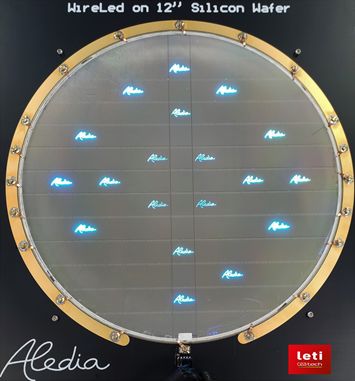
Aledia – Pioneering nanowire microLED’s on 300 mm Wafers
We talk a lot about downsizing. It is, and always will be on the top priority list of the world of electronics. Without smaller sizes, we would never have gotten to this state, where our projects can be housed in a small PCB and ran on an ATTiny mcu. It is one of the most fascinating...
Continue Reading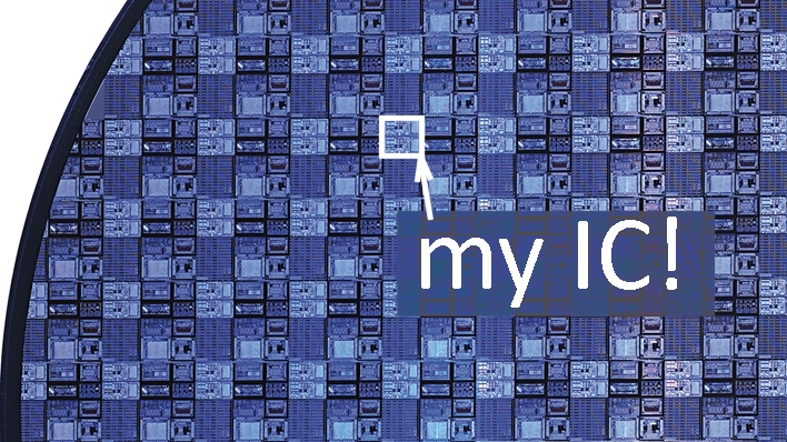
Wafer pooling: low-cost prototyping service for ICs
AMS is providing a fast and cost effective IC prototyping service. by Clemens Valens @ elektormagazine.com: The Full Service Foundry division of ams AG announced its fast and cost-efficient IC prototyping service, known as Multi-Project Wafer (MPW) or shuttle run. The prototyping...
Continue Reading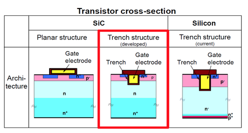
SiC/GaN Poised for Power
by R. Colin Johnson @ eetimes.com: PORTLAND, Ore.—Today Yole Development predicted that power transistors would radically shift from silicon wafers to silicon carbide (SiC) and gallium nitride (GaN) substrates—to achieve higher power in smaller spaces, according to its GaN and...
Continue Reading


