Teardown & analysis of a Keysight InfiniMax III N2802A 25GHz active probe
A teardown & analysis of a Keysight InfiniMax III N2802A 25GHz active probe from TheSignal Path:
In this episode Shahriar takes a close look at one of Keysight (Agilent) InfiniMax III active probes. The model N2802A offers 25GHz of analog bandwidth, 17.5pS of rise time and a total differential input capacitance of 32fF at 10k-Ohm input impedance. The front-end amplifier of this active probe is designed in an in-house InP process, the same process responsible for the front-end of the X-Series Keysight oscilloscopes.
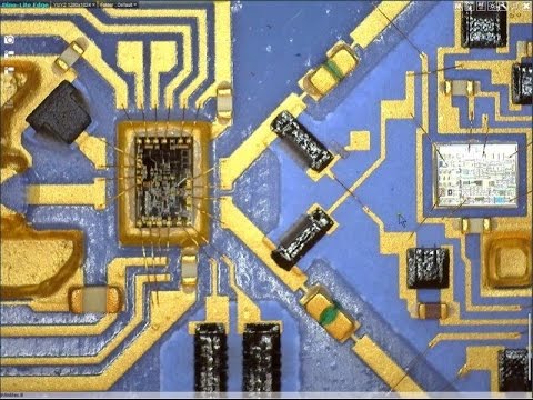
The teardown of the probe shows the control circuitry in the main probe body built around a PIC 16F877 microcontroller coupled to a DAC, EEPROM memory and various high-current and precision op-amps for biasing. The main front-end microwave module reveals the InP ASIC and supporting microwave circuity. There seems to be a dual-path design to provide a large DC common-mode offset capability as well as a high-bandwidth.
Teardown & analysis of a Keysight InfiniMax III N2802A 25GHz active probe – [Link]


