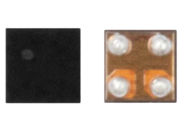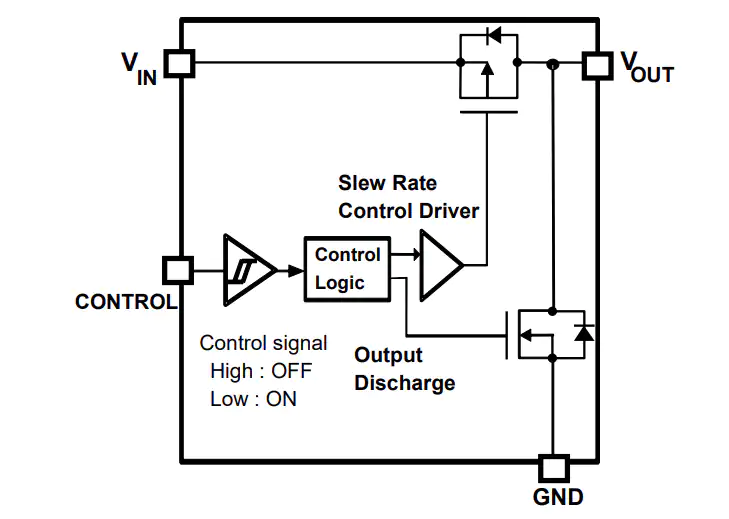
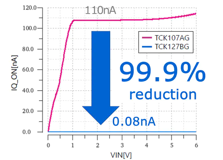
Toshiba TCK12xBG 1A Load Switch ICs are designed for general power management with a slew rate control driver. The TCK12xBG ICs feature ultra-low quiescent current, low switch ON resistance, and a wide 1.0V to 5.5V input operation voltage range. Additionally, the devices provide a quiescent current of 0.08nA and an output current up to 1.0A.
The Toshiba TCK12xBG 1A Load Switch ICs are housed in a 0.35mm pitch ultra-small WCSP4G package (0.645mm x 0.645mm, t: 0.465mm max.) with backside coating that protects from external damage. The TCK12xBG ICs are ideal for portable applications that require high-density board assembly and ultra-low power consumption, such as wearables, smartphones, and IoT modules.
Features
- Wide input operation voltage range of VIN = 1.0V to 5.5V
- Built-in slew rate control driver
- High output current of IOUT = 1A
- Ultra small Quiescent current at IQ = 0.08nA at VIN = 5.5V, VCT = 0V, IOUT =0mA
- Built in slew rate control driver
- Low ON resistance
- RON = 58mΩ (typ.) at VIN = 3.3V, IOUT = -0.5A
- Low standby current (OFF state) : IQ(OFF)+ISD(OFF)=13nA (typ.)
- VIN (OPR)= 1.0V to 5.5V
- Built-in auto-discharge (TCK127BG)
- Active low (TCK128BG), Active high (TCK126BG, TCK127BG)
- WCSP4G Ultra small package with back side coating (0.645mm x 0.645mm, t: 0.465mm max.)
 more information: https://toshiba.semicon-storage.com


