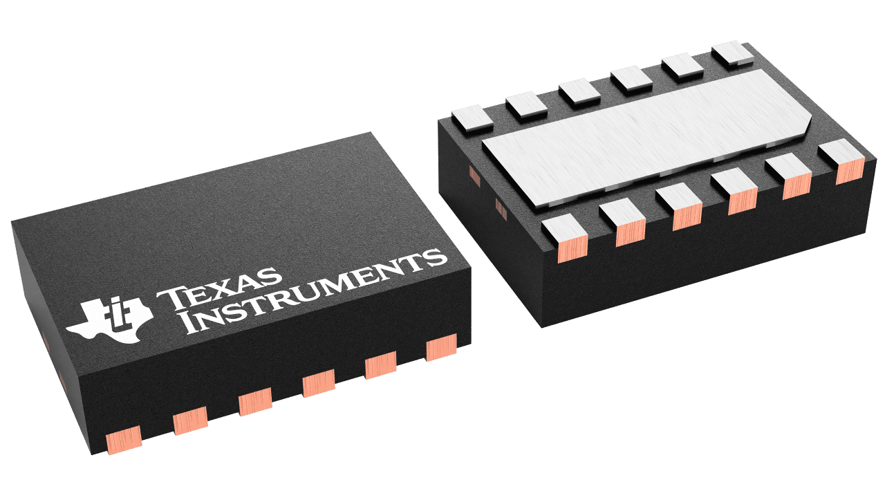
TPS61094 – 60-nA quiescent current bi-directional buck/boost converter with bypass mode
Texas Instruments’ synchronous converter features bypass mode and supercapacitor management
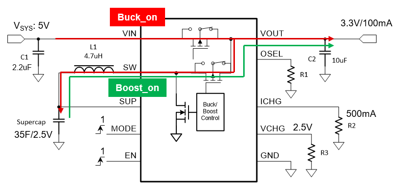
Texas Instruments’ TPS61094 is a synchronous bidirectional buck/boost converter with a bypass switch that provides a power supply solution for smart meters and super capacitor backup power applications. The TPS61094 has a wide input voltage range and output voltage up to 5.5 V. The device works in buck mode and charges the supercapacitor; the charging current and the termination voltage are programmable with two external resistors. When the TPS61094 works in boost mode, the output voltage is programmable with an external resistor. During automatic buck or boost mode (EN = 1, MODE = 1), when the input power supply is applied, the device bypasses the input voltage to the output while it can charge a backup supercapacitor.
When the input power supply is disconnected or lower than the output target voltage, the TPS61094 enters boost mode and regulates output voltage from a backup supercapacitor. The TPS61094 consumes 60 nA quiescent current in this mode. The TPS61094 supports true shutdown mode (EN = 0, MODE = 1) and the forced bypass mode (EN = 0, MODE = 0). In true shutdown mode, the TPS61094 completely disconnects the load from the input supply. When supporting forced bypass mode, the TPS61094 connects the load to the input voltage directly through a bypass switch and consumes 4 nA current to achieve long battery life.
Features
- Input voltage range: 0.7 V to 5.5 V
- Input voltage for startup: 1.8 V (min.)
- Programmable boost output voltage range: 2.7 V to 5.4 V
- Programmable buck charging:
- Termination voltage range: 1.7 V to 5.4 V
- Output current range: 2.5 mA to 600 mA
- Ultra-low quiescent current:
- Boost/buck charging mode: 60 nA
- Forced bypass mode: 4 nA
- Four operation modes controlled by the MODE and EN pins
- Inductor valley current limit: 1.4 A (min.)
- Two MOSFETs: 60 mΩ (LS) and 140 mΩ (HS)
- Bypass switch resistance: 100 mΩ
- Switching frequency: 1 MHz
- Auto-snooze mode operation at light load
- Efficiency:
- Up to 92.3% at VIN = 3 V, VOUT = 3.6 V, and IOUT = 10 μA
- Up to 96.3% at VIN = 3 V, VOUT = 3.6 V, and IOUT = 100 mA
- Output short-circuit protection
- Thermal shutdown protection
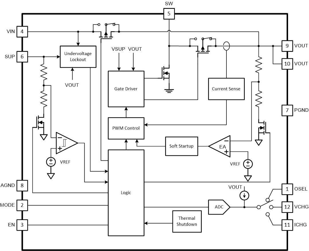
Block Diagram
Application Diagram
more information: https://www.ti.com/product/TPS61094


