Tutorial on the Theory, Design and Characterization of a CMOS Transimpedance Amplifier
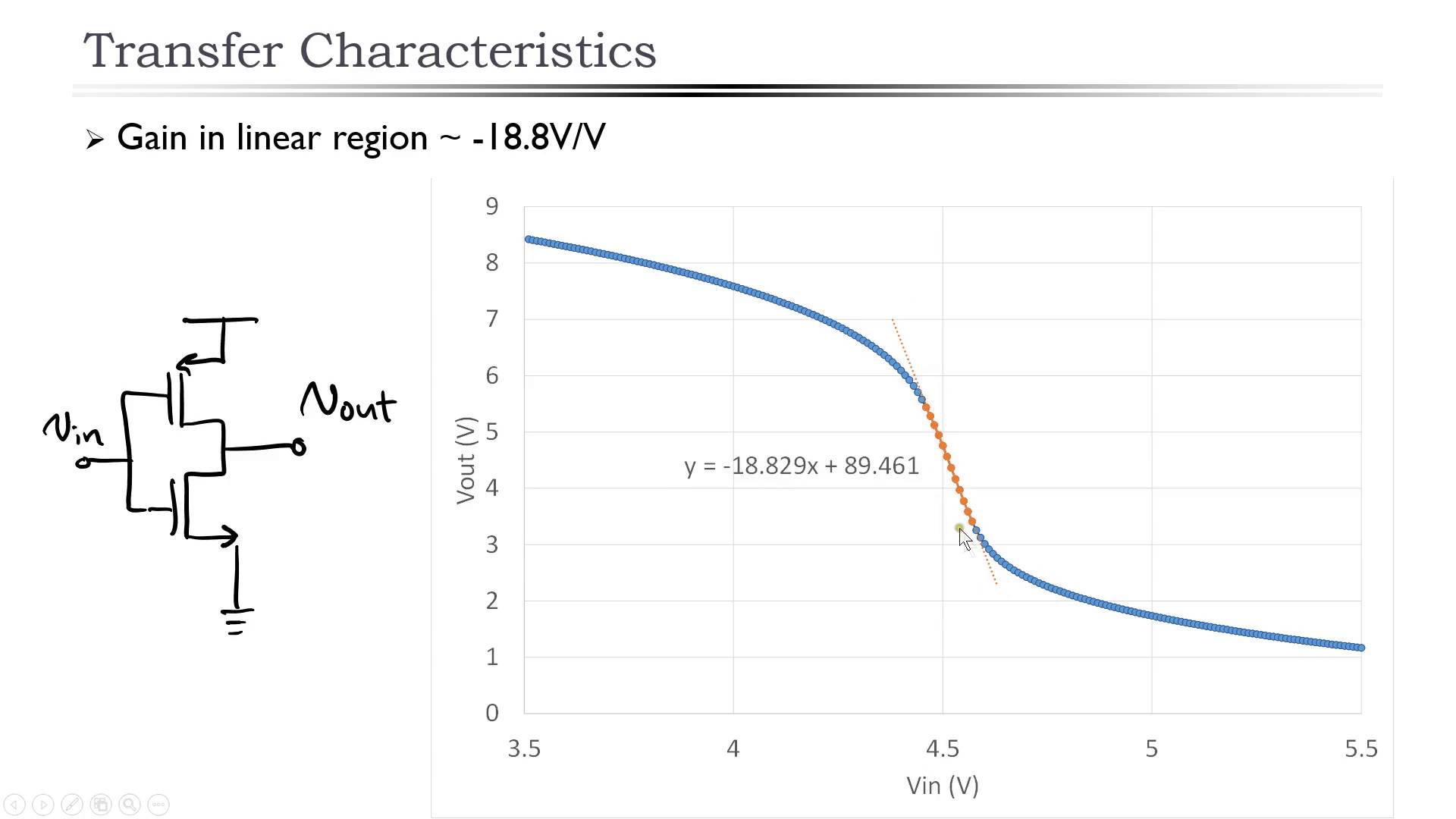
In this episode, Shahriar and Shayan discuss the design and characterization of a deceptively simple CMOS inverter-based transimpedance amplifier. The the large and small signal behavior of the CMOS inverter is discussed and measured using the Keithley 2450 and 2460 source meters. The transient response is also measured using a Keysight MSO-S series oscilloscope.
The small signal gain of the circuit is calculated from small signal parameters which are extracted directly by measuring the devices I/V characteristics. The NMOS/PMOS devices used are from an ADL1105 quad-discrete transistor IC. Through the use of a shunt-shunt feedback, the CMOS amplifiers is converted to a transimpedance amplifier which is capable of amplifying the current from a photo-detector diode by a gain of 30kV/A. The feedback theory is used to calculate the gain of the amplifier. The slides for this tutorial can be downloaded from The Signal Path website.
Tutorial on the Theory, Design and Characterization of a CMOS Transimpedance Amplifier – [Link]


