X-FAB Offers Unique Substrate Coupling Analysis Solution to Address Unwanted Parasitic Effects
Powerful new tool facilitates first-time-right analog & high voltage design implementation in even the most challenging of scenarios.
Continuing to drive innovation in analog/mixed-signal IC fabrication, X-FAB Silicon Foundries SE (http://www.xfab.com/) has announced the introduction of SubstrateXtractor.
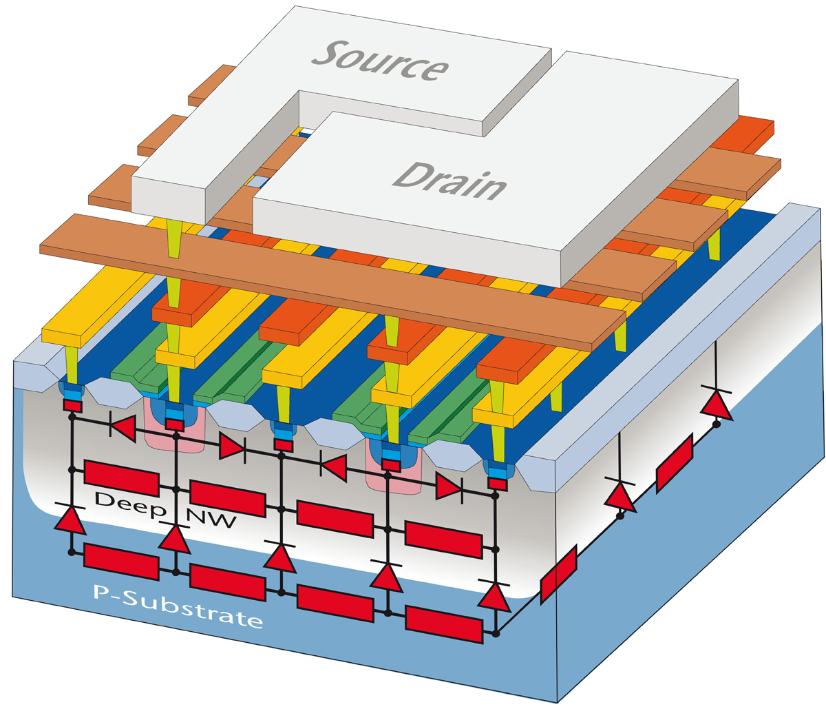
Unwanted substrate couplings can impact modern IC developments, causing parasitic effects that are damaging to overall performance. Engineers have to deal with this by taking a slow and laborious ‘trial and error’ approach, which calls for the allocation of many hours of experienced engineers’ time while numerous different design iterations are made and then experimented with.
The objective of SubstrateXtractor is to change all that. Created in partnership with Swiss EDA software vendor PN Solutions, and based on its innovative PNAware product, this is the semiconductor industry’s first commercially available tool dedicated to addressing the simulation of large signal substrate parasitic effects. Working in conjunction with X-FAB’s established simulation libraries, it allows engineers to investigate where potential substrate coupling issues could occur and make the changes necessary to eliminate them (via better floorplanning, guard rings, etc.) before the initial tape-out has even begun.
Through it, engineers will gain full visibility of all the active and passive elements within the substrate and be able to experiment with different simulations in order to find a design concept that delivers maximum substrate coupling immunity within the project’s particular parametric constraints. Furthermore, they are able to determine the minimum number of substrate contacts and guard rings needed for a project, no matter how complex and sophisticated it is – thereby resulting in more effective utilization of the available area.
“By employing the SubstrateXtractor tool, layout engineers will be able to uncover any adverse substrate effects early on in the development cycle and subsequently mitigate them,” explains Joerg Doblaski, Director of Design Support at X-FAB. “This will make IC implementation procedures far more streamlined and quicker to complete, avoiding the need to rework designs to increase levels of optimization, and resulting in significant cost savings.”
SubstrateXtractor is set to dramatically reduce the number of design iterations required – leading to much lower engineering overheads. This results in a faster time to market making a first-time-right analog design possible. From now onwards this functionality will be integrated into X-FAB’s process design kit (PDK) and available for use with the company’s popular XH018 (https://www.xfab.com/technology/cmos/018-um-xh018/) high voltage 0.18µm mixed-signal CMOS offering. A version for the power management process XP018 will soon follow. A detailed webinar on this valuable new tool will be hosted on May 22nd and 23rd. For details and to register, click here (https://register.gotowebinar.com/rt/7742535881476974860).


